EP0335074A2 - Alignment mark system - Google Patents
Alignment mark system Download PDFInfo
- Publication number
- EP0335074A2 EP0335074A2 EP89101371A EP89101371A EP0335074A2 EP 0335074 A2 EP0335074 A2 EP 0335074A2 EP 89101371 A EP89101371 A EP 89101371A EP 89101371 A EP89101371 A EP 89101371A EP 0335074 A2 EP0335074 A2 EP 0335074A2
- Authority
- EP
- European Patent Office
- Prior art keywords
- wafer
- alignment
- silicon
- isolation
- alignment marks
- Prior art date
- Legal status (The legal status is an assumption and is not a legal conclusion. Google has not performed a legal analysis and makes no representation as to the accuracy of the status listed.)
- Withdrawn
Links
Images

Classifications
-
- G—PHYSICS
- G03—PHOTOGRAPHY; CINEMATOGRAPHY; ANALOGOUS TECHNIQUES USING WAVES OTHER THAN OPTICAL WAVES; ELECTROGRAPHY; HOLOGRAPHY
- G03F—PHOTOMECHANICAL PRODUCTION OF TEXTURED OR PATTERNED SURFACES, e.g. FOR PRINTING, FOR PROCESSING OF SEMICONDUCTOR DEVICES; MATERIALS THEREFOR; ORIGINALS THEREFOR; APPARATUS SPECIALLY ADAPTED THEREFOR
- G03F9/00—Registration or positioning of originals, masks, frames, photographic sheets or textured or patterned surfaces, e.g. automatically
- G03F9/70—Registration or positioning of originals, masks, frames, photographic sheets or textured or patterned surfaces, e.g. automatically for microlithography
-
- H—ELECTRICITY
- H10—SEMICONDUCTOR DEVICES; ELECTRIC SOLID-STATE DEVICES NOT OTHERWISE PROVIDED FOR
- H10W—GENERIC PACKAGES, INTERCONNECTIONS, CONNECTORS OR OTHER CONSTRUCTIONAL DETAILS OF DEVICES COVERED BY CLASS H10
- H10W46/00—Marks applied to devices, e.g. for alignment or identification
-
- H—ELECTRICITY
- H10—SEMICONDUCTOR DEVICES; ELECTRIC SOLID-STATE DEVICES NOT OTHERWISE PROVIDED FOR
- H10W—GENERIC PACKAGES, INTERCONNECTIONS, CONNECTORS OR OTHER CONSTRUCTIONAL DETAILS OF DEVICES COVERED BY CLASS H10
- H10W46/00—Marks applied to devices, e.g. for alignment or identification
- H10W46/101—Marks applied to devices, e.g. for alignment or identification characterised by the type of information, e.g. logos or symbols
-
- H—ELECTRICITY
- H10—SEMICONDUCTOR DEVICES; ELECTRIC SOLID-STATE DEVICES NOT OTHERWISE PROVIDED FOR
- H10W—GENERIC PACKAGES, INTERCONNECTIONS, CONNECTORS OR OTHER CONSTRUCTIONAL DETAILS OF DEVICES COVERED BY CLASS H10
- H10W46/00—Marks applied to devices, e.g. for alignment or identification
- H10W46/301—Marks applied to devices, e.g. for alignment or identification for alignment
-
- H—ELECTRICITY
- H10—SEMICONDUCTOR DEVICES; ELECTRIC SOLID-STATE DEVICES NOT OTHERWISE PROVIDED FOR
- H10W—GENERIC PACKAGES, INTERCONNECTIONS, CONNECTORS OR OTHER CONSTRUCTIONAL DETAILS OF DEVICES COVERED BY CLASS H10
- H10W46/00—Marks applied to devices, e.g. for alignment or identification
- H10W46/501—Marks applied to devices, e.g. for alignment or identification for use before dicing
Definitions
- This invention relates to a method for manufacturing an semiconductor device and the resulting device.
- this invention relates to the structure and process of alignment marks to be used in mixed lithography systems for making semiconductor devices.
- lithography schemes are employed to produce a wide variety of devices.
- the most common are optical, electron beam and X-ray. All have unique attributes and disadvantages.
- the art has proposed the mixing of these schemes to take advantage of the ef-ficiencies and accuracy offered by them in various stages of device manufacturing.
- U.S. Patent 4,612,274 describes a method for using a combination of electron beam (E-beam) and photolithography in the manufacture of an acoustic wave device.
- the E-beam is used for purposes of writing fine lines which are required in an acoustic wave device while optical lithography is employed to delineate the large scale pad areas.
- IBM Technical Disclosure Bulletin, Volume 1, No. 8, pp 3176-3177 (January 1979) relates to a combined E-beam and X-ray lithography process in the manufacture of semiconductor devices.
- This prior art recognizes that E-beam provides unique alignment capabilities but, at the same time, notes the inherent problems which exist when mixed lithography process are used in terms of maintaining proper registration alignment.
- the process employed in this TDB employs an alignment mark which is formed in the semiconductor wafer with that align ment mark maintained visible for E-beam registration by evaporating through metal topography which is used as a X-ray absorber for subsequent processing or maintaining rough alignment by means of visible topography in the X-ray absorber layer.
- some comprise in the E-beam alignment accuracy results when relying on visible topography.
- the overlay is not only a second order alignment which, as indicated, is itself a problem, but is also limited by the alignment of the optical system. Stated differently the alignment which is achieved cannot be better than the alignment of the optical system to the common zero level. As such, even when using E-beam systems for purposes of a portion of the fabrication process, the level of registration is inherently limited to that which is achieved by the optical alignment. Thus, within the prior art a need exists to improve overlay accuracy when matching an E-beam lithography system to an optical lithography tool.
- the typical optical lithography system is capable of aligning to marks which are defined at the ROX level.
- the profile of the isolation oxide is in of itself sufficient to be processed optically. Such however is not true for the E-beam system.
- Two problems arise when attempting to align to the isolation oxide profile. First, the slope of the oxide due to the so-called birds beak phenomena, does not permit sufficient contrast in signal as that mark is scanned. Secondly, the height difference in the active region to the top of the oxide is not sufficient. To date, no technique has been proposed or used which allows both the E-beam and an optical lithography scheme to align directly to the ROX level.
- Yet another object of this invention is to provide the improved alignment scheme which reduces the inherent order of magnitude difference when alignment is predicated on common zero level approaches.
- a further object of this invention is to provide improved alignment marks for mixed E-beam and optical lithography in the production of FET transistor structures and in particular to use a E-beam system in writing the gate level in the FET process.
- Yet another object of this invention is to provide an alignment mark strategy which allows the E-beam system to align to the isolation level when the E-beam system is used to write the emitter level lines in a bipolar process.
- Alignment marks are exposed along with data, that is the actual device data on the ROX level during device processing.
- the polarity is chosen so that the silicon nitrite is left on the marks after etching of the ROX level.
- the wafer is then processed in a standard manner to produce the devices up to and including the removal of silicon nitrite after oxidation. See, for example, "VLSI Technology", S.M. S, McGraw-Hill Book Company, Chapter 2 (1983). At this point in the process the marks will be silicon surrounded by isolation oxide.
- the wafer is then patterned with an appropriate resist so that only the alignment marks are unprotected by the resist.
- the ROX then is used as a self aligning mask and the wafer is etched in a standard manner for zero level alignment.
- the resulting alignment structure is a series of tren ches 1-2 ⁇ m deep surrounded by ROX. Such provides a very sharp transition for the E-beam to scan and provide the necessary back scatter electron wavelength to accurately pick off the edges of the alignment marks.
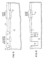
- FIG. 1A illustrates a typical wafer 10 having a series of alignment zones 12 while nine zones are illustrated it will be understood that such are positioned on the wafer purely as a function of a location to achieve the necessary alignment depending on the processing and equipment which is used. More strictlyover, Fig. 1A represents an exaggeration since the "real estate" occupied by the alignment zones 12 is, in reality, very small in comparison to the surface 14 of the wafer 10 which is used for device processing. The use of alignment marks per se on semiconductor wafers is established in the art. U.S.
- Patent 4,486,857 describes a scheme by which alignment marks are positioned on a side-by-side basis with individual integrated circuit structures.
- Fig. 1A illustrates merely one of a variety of design alternatives for the placement of alignment mark zones vis-a-vis device processing areas.
- FIG. 1B the enlargement of a typical alignment mark zone is depicted.
- An alignment pattern in the zone 12 comprises a series of eight features. Those features are grouped in pairs and comprise trenches 16 etched into the surface of the wafer 10 in one orientation and pairs of trenches 18 etched into the silicon in an orthogonal direction.
- the alignment pattern depicted in Fig. 1B provides therefore a series of aligned trench walls provide the necessary relief for generation of back scattered electrons necessary to produce the edge-to-edge waveform transitions necessary to center the electron beam.
- Fig. 2A onto a silicon substrate 10 approximately 100 angstroms of SiO2 is first deposited. Then, approximately 1000 angstroms Si3N4 22 is overlaid on the oxide.
- Fig. 2B illustrates the patterning of the alignment mark area of the wafer 10 after removal of the masks and the like. It would be understood that depending on the process used, at this step, in the device area regions would typically be formed. Reference is made to IBM TDB, Volume 15, No. 6, pp 1823-1825 (November 1972) which describes a series of steps used to produce FET structure. In accordance with this invention the polarity is chosen so that the Si3N4 remains on the marks after etching of the isolation level. Such is illustrated in Fig. 2B.
- etching for example reactive ion etching (RIE) up to and including the removal of the Si3N4 following oxidation.
- RIE reactive ion etching
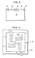
- the processing of the marks at this point is illustrated in Fig. 3.
- the alignment pattern is therefore silicon surrounded by isolation level oxide (ROX) 24.
- the marks themselves will be created in the silicon zones 26 existing between the ROX 24.
- the wafer 10 is then patterned with a suitable resist 28 so that only the alignment marks are unprotected by the resist.
- Fig. 4 illustrates the zone 30 which is left unprotected by the resist 28.
- Fig. 5 illustrates in a side view how the patterning occurs so the area which is used to produce the alignment marks remains uncovered.
- the ROX is thus used as the mask for etching into the silicon 10.
- the silicon is etched using standard techniques to produce a series of trenches 32 illustrated in Fig. 6. Those trenches have a depth D in the range of 1-2 ⁇ m.
- the patterning by the resist 28 protects the remainder of the wafer. It will be appreciated that the figures do not scale the device and alignment regions. For purposes of explanation, the alignment regions have been deliberately enlarged to illustrate the principles of this invention.
- the alignment marks are in alignment with the gate level polysilicon forming the FET structure 34 as illustrated in Fig. 6 with the isolation level in that same FET transistor process.
- This alignment provides a significant improvement in terms of packing density since it allows gain in overlay accuracy in the range of 0.2-0.3 ⁇ m improvement. Such therefore facilitates the use of a E-beam to generate fine lines and therefore higher density the definition of the FET gate structure.
- Processing then proceeds in accordance with known techniques utilizing the alignment marks as produced by this invention to align both E-beam and optical devices.
- the E-beam could be used to write fine lines while optical processing is employed as a conventional lithography step.
- the system however aligns to the level of accuracy of the device being employed and not to a second order.
- this technique is not limited to the FET process when in fact is is usable for any transistor process whether it is FET, bipolar/Si or GaAs.
- a ROX level is used as the first lithography level.
- Trenches themselves provide the necessary height difference in the alignment marks to provide sharp transition in back scatter electron level.
- the system is not dependent on a second order alignment yet it allows the E-beam system to align to its own marks while having the optical lithography align to the profile of the oscillation oxide.
- this improved alignment mark structure/process allows for the first order alignment of an E-beam system to the isolation level (ROX) during the subsequent lithography levels.
- This technique can be used to produce any type of integrated circuit/transistor that requires a ROX structure.
- the ROX level does not need to be the first lithography level, but it would be preferred. Also, this mark would be good for all levels exposed after the ROX level and not limited to the poly or the emitter level, for example contact, metal and via levels.
Landscapes
- Physics & Mathematics (AREA)
- General Physics & Mathematics (AREA)
- Exposure Of Semiconductors, Excluding Electron Or Ion Beam Exposure (AREA)
- Exposure And Positioning Against Photoresist Photosensitive Materials (AREA)
Abstract
Description
- This invention relates to a method for manufacturing an semiconductor device and the resulting device. In particular, this invention relates to the structure and process of alignment marks to be used in mixed lithography systems for making semiconductor devices.
- Within the prior art lithography schemes are employed to produce a wide variety of devices. The most common are optical, electron beam and X-ray. All have unique attributes and disadvantages. The art has proposed the mixing of these schemes to take advantage of the ef-ficiencies and accuracy offered by them in various stages of device manufacturing. For example U.S. Patent 4,612,274 describes a method for using a combination of electron beam (E-beam) and photolithography in the manufacture of an acoustic wave device. The E-beam is used for purposes of writing fine lines which are required in an acoustic wave device while optical lithography is employed to delineate the large scale pad areas.
- IBM Technical Disclosure Bulletin, Volume 1, No. 8, pp 3176-3177 (January 1979) relates to a combined E-beam and X-ray lithography process in the manufacture of semiconductor devices. This prior art recognizes that E-beam provides unique alignment capabilities but, at the same time, notes the inherent problems which exist when mixed lithography process are used in terms of maintaining proper registration alignment. The process employed in this TDB employs an alignment mark which is formed in the semiconductor wafer with that align ment mark maintained visible for E-beam registration by evaporating through metal topography which is used as a X-ray absorber for subsequent processing or maintaining rough alignment by means of visible topography in the X-ray absorber layer. As recognized however some comprise in the E-beam alignment accuracy results when relying on visible topography.
- Other techniques for providing a registration mark for use with E-beam systems is disclosed in U.S. Patent 3,710,101 and in IBM TDB, Volume 27, No. 1B, pp 686-688 (June 1984). In any scheme employing mixed lithography it is desirable to use the electron beam system for achieving maximum resolution on the critical device levels. The electron beam system is capable of achieving dimensional control that reaches 0.1µm. In contrast, optical lithography begins to reach its limit at between 0.75 to 0.50 µm and requires a very small process window. Along with dimensional control, electron beam lithography also has the added advantage of superior overlay capability. To fully take advantage of the electron beam system, it is important that the critical device levels that will be written by the electron beam system, be aligned directly to the optically exposed isolation (ROX) level.
- In the case of typical optical/E-beam mixed lithography processes, it is common to use a so-called "common zero level" alignment approach. In this technique, once the zero level has been established subsequent levels are written by both the optical and E-beam systems aligned to that zero level. This technique is limited by the fact that all levels are registered using second order alignment. A second order alignment is defined as the registration of one level to another indirectly aligning to a common level. Second order alignments have associated with them a higher degree of overlay error due, in part, to the summation of errors which exist for each of the two levels.
- When employing a common zero level process the overlay is not only a second order alignment which, as indicated, is itself a problem, but is also limited by the alignment of the optical system. Stated differently the alignment which is achieved cannot be better than the alignment of the optical system to the common zero level. As such, even when using E-beam systems for purposes of a portion of the fabrication process, the level of registration is inherently limited to that which is achieved by the optical alignment. Thus, within the prior art a need exists to improve overlay accuracy when matching an E-beam lithography system to an optical lithography tool.
- Given the clear advantages of E-beam lithography systems over optical systems in terms of the ability to register device levels more accurately, it would be clearly advantageous in a mixed lithography scheme to align to a particular level directly to the other level of interest. Such would be defined as a first order alignment. For example it would be preferable in the FET transistor process to align the gate level (poly) to the isolation level (ROX). Another example would be alignment of the emitter level to the ROX level in the case of a bipolar technique. In either, when the E-beam lithography system is aligned directly to the ROX level, the exposure system is then being used to its best advantage. That is, alignment can occur at the submicron level. Such achieves important advantages in that the optical system is then used to enhance through-put and the E-beam system may be used to maximize alignment and resolution.
- While such desirabilities would find application in a pure E-beam system, problems occur in mixed lithography environments. The typical optical lithography system is capable of aligning to marks which are defined at the ROX level. The profile of the isolation oxide is in of itself sufficient to be processed optically. Such however is not true for the E-beam system. Two problems arise when attempting to align to the isolation oxide profile. First, the slope of the oxide due to the so-called birds beak phenomena, does not permit sufficient contrast in signal as that mark is scanned. Secondly, the height difference in the active region to the top of the oxide is not sufficient. To date, no technique has been proposed or used which allows both the E-beam and an optical lithography scheme to align directly to the ROX level.
- Therefore, it is an object of this invention to define an improved system of alignment for E-beam and optical mixed lithography systems.
- It is further object of this invention to provide a scheme by which alignment marks may be produced at the isolation level in an early stage of semiconductor device development which will enable the electron beam system to align direct to it.
- Yet another object of this invention is to provide the improved alignment scheme which reduces the inherent order of magnitude difference when alignment is predicated on common zero level approaches.
- A further object of this invention is to provide improved alignment marks for mixed E-beam and optical lithography in the production of FET transistor structures and in particular to use a E-beam system in writing the gate level in the FET process.
- Yet another object of this invention is to provide an alignment mark strategy which allows the E-beam system to align to the isolation level when the E-beam system is used to write the emitter level lines in a bipolar process.
- These and other objects of this invention are accomplished in the method which able to align directly to an optically written level with an electron beam system, the alignment of the two levels to each other limited only by the alignment accuracy of the E-beam tool. The method provides a technique by which alignment marks are produced at the isolation level which enables the E-beam system to align directly to it. Thus in accordance with this invention no second order alignment is required.
- Alignment marks are exposed along with data, that is the actual device data on the ROX level during device processing. The polarity is chosen so that the silicon nitrite is left on the marks after etching of the ROX level. The wafer is then processed in a standard manner to produce the devices up to and including the removal of silicon nitrite after oxidation. See, for example, "VLSI Technology", S.M. S, McGraw-Hill Book Company, Chapter 2 (1983). At this point in the process the marks will be silicon surrounded by isolation oxide. The wafer is then patterned with an appropriate resist so that only the alignment marks are unprotected by the resist. The ROX then is used as a self aligning mask and the wafer is etched in a standard manner for zero level alignment. See, "VLSI Technology", S.M. S, McGraw-Hill Book Company, Chapter 8, (1983). The result is marks which appear similar to those of standard zero level marks but are bordered by the ROX. Since the ROX is used as the mask the alignment marks are in perfect alignment to the ROX pattern because they were exposed along with it.
- The resulting alignment structure is a series of tren ches 1-2µm deep surrounded by ROX. Such provides a very sharp transition for the E-beam to scan and provide the necessary back scatter electron wavelength to accurately pick off the edges of the alignment marks. This invention will be described by reference to the attached drawings and the description of the preferred embodiment that follows.
- Fig. 1A is a schematic top view of a semiconductor wafer showing a typical location of alignment marks;
- Fig. 1B is a partial view of the alignment mark topography of Fig. 1A.
- Figs. 2A and 2B are schematic cross-sectional views of the process used to form the isolation oxide in device processing.
- Fig. 3 is a schematic cross-sectional view of the ROX pattern produced.
- Figs. 4 and 5 are respectively a schematic plan view and cross-sectional view of the patterning with resist in accordance with the next step of the process.
- Fig. 6 is a schematic cross-sectional view illustrating a composite of alignment marks and a portion of a device structure so produced.
- Referring now to Fig.s 1A and 1B the basic topography for producing alignment marks on a silicon wafer is depicted. Fig. 1A illustrates a
typical wafer 10 having a series ofalignment zones 12 while nine zones are illustrated it will be understood that such are positioned on the wafer purely as a function of a location to achieve the necessary alignment depending on the processing and equipment which is used. Moreover, Fig. 1A represents an exaggeration since the "real estate" occupied by thealignment zones 12 is, in reality, very small in comparison to thesurface 14 of thewafer 10 which is used for device processing. The use of alignment marks per se on semiconductor wafers is established in the art. U.S. Patent 4,486,857 describes a scheme by which alignment marks are positioned on a side-by-side basis with individual integrated circuit structures. Thus, Fig. 1A illustrates merely one of a variety of design alternatives for the placement of alignment mark zones vis-a-vis device processing areas. - Referring to Fig. 1B the enlargement of a typical alignment mark zone is depicted. An alignment pattern in the
zone 12 comprises a series of eight features. Those features are grouped in pairs and comprisetrenches 16 etched into the surface of thewafer 10 in one orientation and pairs oftrenches 18 etched into the silicon in an orthogonal direction. The alignment pattern depicted in Fig. 1B provides therefore a series of aligned trench walls provide the necessary relief for generation of back scattered electrons necessary to produce the edge-to-edge waveform transitions necessary to center the electron beam. - The process used to produce the pattern illustrated in Fig. 1B will now be described by reference to Fig.s 2-6. The description is for the manufacture of an FET. This is for purposes of illustration of the use of this invention in conjunction with an established process. The invention is not limited to the making of FET's. It will be further understood that with respect to certain of the processing steps delineated and described vis-a-vis those figures the processing of one parallel set of trenches will be described, but that the appropriate patterning produces a composite alignment mark structure illustrated in Fig. 1B.
- Referring now to Fig. 2A onto a
silicon substrate 10 approximately 100 angstroms of SiO₂ is first deposited. Then, approximately 1000angstroms Si₃N₄ 22 is overlaid on the oxide. Referring to Fig. 2B the alignment marks to be formed are exposed along with the device data on thesilicon substrate 10 using conventional patterning techniques. Fig. 2B illustrates the patterning of the alignment mark area of thewafer 10 after removal of the masks and the like. It would be understood that depending on the process used, at this step, in the device area regions would typically be formed. Reference is made to IBM TDB, Volume 15, No. 6, pp 1823-1825 (November 1972) which describes a series of steps used to produce FET structure. In accordance with this invention the polarity is chosen so that the Si₃N₄ remains on the marks after etching of the isolation level. Such is illustrated in Fig. 2B. - Device processing then proceeds utilizing etching, for example reactive ion etching (RIE) up to and including the removal of the Si₃N₄ following oxidation. The processing of the marks at this point is illustrated in Fig. 3. The alignment pattern is therefore silicon surrounded by isolation level oxide (ROX) 24. The marks themselves will be created in the
silicon zones 26 existing between theROX 24. - In accordance with this process, the
wafer 10 is then patterned with a suitable resist 28 so that only the alignment marks are unprotected by the resist. Fig. 4 illustrates thezone 30 which is left unprotected by the resist 28. Fig. 5 illustrates in a side view how the patterning occurs so the area which is used to produce the alignment marks remains uncovered. As can be appreciated the ROX is thus used as the mask for etching into thesilicon 10. - Utilizing the patterned resist structure having the resist 28 and
isolation oxide 24 acting as a mask, the silicon is etched using standard techniques to produce a series oftrenches 32 illustrated in Fig. 6. Those trenches have a depth D in the range of 1-2µm. During the formation of those trenches which form a pair of alignment marks, for example,trenches - Thus, in accordance with this invention all that is required is the introduction of a non-critical masking step to produce the resist pattern illustrated in Fig.s 4 and 5 prior to etching to produce the trenches illustrated in Fig. 6.
- By this technique the alignment marks are in alignment with the gate level polysilicon forming the
FET structure 34 as illustrated in Fig. 6 with the isolation level in that same FET transistor process. This alignment provides a significant improvement in terms of packing density since it allows gain in overlay accuracy in the range of 0.2-0.3µm improvement. Such therefore facilitates the use of a E-beam to generate fine lines and therefore higher density the definition of the FET gate structure. - Similar improvements can also be achieved by aligning the emitter to the ROX in the case of bipolar devices.
- Processing then proceeds in accordance with known techniques utilizing the alignment marks as produced by this invention to align both E-beam and optical devices. For example, the E-beam could be used to write fine lines while optical processing is employed as a conventional lithography step. The system however aligns to the level of accuracy of the device being employed and not to a second order.
- It can be appreciated that this technique is not limited to the FET process when in fact is is usable for any transistor process whether it is FET, bipolar/Si or GaAs. In all of those processes, a ROX level is used as the first lithography level. By the use of this invention the inherent disadvantages of prior art systems are overcome. Trenches themselves provide the necessary height difference in the alignment marks to provide sharp transition in back scatter electron level. The system is not dependent on a second order alignment yet it allows the E-beam system to align to its own marks while having the optical lithography align to the profile of the oscillation oxide.
- Thus, this improved alignment mark structure/process allows for the first order alignment of an E-beam system to the isolation level (ROX) during the subsequent lithography levels.
- This technique can be used to produce any type of integrated circuit/transistor that requires a ROX structure. The ROX level does not need to be the first lithography level, but it would be preferred. Also, this mark would be good for all levels exposed after the ROX level and not limited to the poly or the emitter level, for example contact, metal and via levels.
- It is apparent that modifications of this invention may be practiced without departing from the essential scope thereof.
Claims (10)
providing a silicon wafer (10) having a silicon dioxide (20) and silicon nitride film (22) stack thereon,
exposing an isolation pattern (24) of data and alignment marks on said film stack,
processing said wafer to define a pattern of alignment mark positions on said silicon bordered by said isolation oxide (24),
patterning said wafer with a resist (28) so that only said alignment mark positions are unprotected, and
etching said wafer to an appropriate depth using said isolation oxide (24) as a mask whereby an alignment mark structure (32) is created in said silicon wafer bordered by said isolation oxide (24) and in alignment therewith.
a series of semiconductor devices produced on said wafer, and a series of alignment marks (32) etched into said wafer in alignment with and bordered by an isolation level oxide (24).
Applications Claiming Priority (2)
| Application Number | Priority Date | Filing Date | Title |
|---|---|---|---|
| US07/173,832 US4893163A (en) | 1988-03-28 | 1988-03-28 | Alignment mark system for electron beam/optical mixed lithography |
| US173832 | 1988-03-28 |
Publications (2)
| Publication Number | Publication Date |
|---|---|
| EP0335074A2 true EP0335074A2 (en) | 1989-10-04 |
| EP0335074A3 EP0335074A3 (en) | 1990-07-04 |
Family
ID=22633693
Family Applications (1)
| Application Number | Title | Priority Date | Filing Date |
|---|---|---|---|
| EP89101371A Withdrawn EP0335074A3 (en) | 1988-03-28 | 1989-01-27 | Alignment mark system |
Country Status (3)
| Country | Link |
|---|---|
| US (1) | US4893163A (en) |
| EP (1) | EP0335074A3 (en) |
| JP (1) | JPH0210716A (en) |
Cited By (7)
| Publication number | Priority date | Publication date | Assignee | Title |
|---|---|---|---|---|
| EP0478072A1 (en) * | 1990-09-28 | 1992-04-01 | Koninklijke Philips Electronics N.V. | Process for making alignment marks for masks |
| EP0448471A3 (en) * | 1990-03-20 | 1993-05-26 | Fujitsu Limited | Method of planarizing metal layer |
| DE19534784C1 (en) * | 1995-09-19 | 1997-04-24 | Siemens Ag | Semiconductor circuit element and method for its manufacture |
| EP0781660A1 (en) * | 1995-12-26 | 1997-07-02 | Oki Electric Industry Co., Ltd. | LED array alignment |
| EP0892433A1 (en) * | 1997-07-15 | 1999-01-20 | International Business Machines Corporation | Method of forming an alignment mark in a semiconductor structure |
| WO2002046843A1 (en) * | 2000-12-08 | 2002-06-13 | Dalsa Semiconductor Inc. | Method of aligning a photolithographic mask to a crystal plane |
| CN108470691A (en) * | 2018-03-29 | 2018-08-31 | 上海华力集成电路制造有限公司 | The manufacturing method of the laminated measurement pattern of polysilicon for contact hole alignment |
Families Citing this family (37)
| Publication number | Priority date | Publication date | Assignee | Title |
|---|---|---|---|---|
| JP2831847B2 (en) * | 1990-11-29 | 1998-12-02 | 株式会社東芝 | Method for manufacturing semiconductor device |
| US5314837A (en) * | 1992-06-08 | 1994-05-24 | Analog Devices, Incorporated | Method of making a registration mark on a semiconductor |
| US5311061A (en) * | 1993-05-19 | 1994-05-10 | Motorola Inc. | Alignment key for a semiconductor device having a seal against ionic contamination |
| JP2595885B2 (en) * | 1993-11-18 | 1997-04-02 | 日本電気株式会社 | Semiconductor device and manufacturing method thereof |
| DE4341171C2 (en) * | 1993-12-02 | 1997-04-17 | Siemens Ag | Method for producing an integrated circuit arrangement |
| JP3156896B2 (en) * | 1994-01-28 | 2001-04-16 | 富士通株式会社 | Semiconductor device manufacturing method and semiconductor device manufactured by such manufacturing method |
| US5469263A (en) * | 1994-07-01 | 1995-11-21 | Motorola, Inc. | Method for alignment in photolithographic processes |
| US5777392A (en) * | 1995-03-28 | 1998-07-07 | Nec Corporation | Semiconductor device having improved alignment marks |
| US5702567A (en) * | 1995-06-01 | 1997-12-30 | Kabushiki Kaisha Toshiba | Plurality of photolithographic alignment marks with shape, size and spacing based on circuit pattern features |
| US5861654A (en) * | 1995-11-28 | 1999-01-19 | Eastman Kodak Company | Image sensor assembly |
| DE69632228T2 (en) * | 1995-07-13 | 2005-04-14 | Eastman Kodak Co. | Image sensor with a carrier housing |
| US5700732A (en) * | 1996-08-02 | 1997-12-23 | Micron Technology, Inc. | Semiconductor wafer, wafer alignment patterns and method of forming wafer alignment patterns |
| US5786260A (en) * | 1996-12-16 | 1998-07-28 | Taiwan Semiconductor Manufacturing Company, Ltd. | Method of fabricating a readable alignment mark structure using enhanced chemical mechanical polishing |
| US5956564A (en) * | 1997-06-03 | 1999-09-21 | Ultratech Stepper, Inc. | Method of making a side alignment mark |
| US6020249A (en) * | 1997-07-10 | 2000-02-01 | Taiwan Semiconductor Manufacturing Company | Method for photo alignment after CMP planarization |
| US6163065A (en) * | 1997-12-31 | 2000-12-19 | Intel Corporation | Energy-absorbing stable guard ring |
| US6249036B1 (en) * | 1998-03-18 | 2001-06-19 | Advanced Micro Devices, Inc. | Stepper alignment mark formation with dual field oxide process |
| US6037671A (en) | 1998-11-03 | 2000-03-14 | Advanced Micro Devices, Inc. | Stepper alignment mark structure for maintaining alignment integrity |
| US6271602B1 (en) * | 1999-08-31 | 2001-08-07 | Advanced Micro Devices, Inc. | Method for reducing the susceptibility to chemical-mechanical polishing damage of an alignment mark formed in a semiconductor substrate |
| US6294018B1 (en) * | 1999-09-15 | 2001-09-25 | Lucent Technologies | Alignment techniques for epitaxial growth processes |
| JP4407785B2 (en) * | 2000-10-24 | 2010-02-03 | ソニー株式会社 | Semiconductor device and inspection method thereof |
| US20080000495A1 (en) * | 2001-12-07 | 2008-01-03 | Eric Hansen | Apparatus and method for single substrate processing |
| US6875624B2 (en) * | 2002-05-08 | 2005-04-05 | Taiwan Semiconductor Manufacturing Co. Ltd. | Combined E-beam and optical exposure semiconductor lithography |
| US7800097B2 (en) * | 2004-12-13 | 2010-09-21 | Panasonic Corporation | Semiconductor device including independent active layers and method for fabricating the same |
| US7259373B2 (en) * | 2005-07-08 | 2007-08-21 | Nexgensemi Holdings Corporation | Apparatus and method for controlled particle beam manufacturing |
| US7687925B2 (en) | 2005-09-07 | 2010-03-30 | Infineon Technologies Ag | Alignment marks for polarized light lithography and method for use thereof |
| WO2008140585A1 (en) | 2006-11-22 | 2008-11-20 | Nexgen Semi Holding, Inc. | Apparatus and method for conformal mask manufacturing |
| US7550361B2 (en) * | 2007-01-02 | 2009-06-23 | International Business Machines Corporation | Trench structure and method for co-alignment of mixed optical and electron beam lithographic fabrication levels |
| JP5571283B2 (en) * | 2007-12-25 | 2014-08-13 | ローム株式会社 | Semiconductor device |
| US10566169B1 (en) | 2008-06-30 | 2020-02-18 | Nexgen Semi Holding, Inc. | Method and device for spatial charged particle bunching |
| US10991545B2 (en) | 2008-06-30 | 2021-04-27 | Nexgen Semi Holding, Inc. | Method and device for spatial charged particle bunching |
| CN102280367B (en) * | 2010-06-08 | 2013-09-25 | 旺宏电子股份有限公司 | Method for protecting alignment marks and semiconductor element formed by the method |
| US9646902B2 (en) | 2013-08-12 | 2017-05-09 | Taiwan Semiconductor Manufacturing Company Limited | Paired edge alignment |
| JP6198337B2 (en) * | 2014-06-25 | 2017-09-20 | ローム株式会社 | Semiconductor device |
| US9994042B2 (en) * | 2015-04-16 | 2018-06-12 | Victor Manuel Sud Arce | Substrates and method for print engravings |
| US12493005B1 (en) | 2022-06-07 | 2025-12-09 | Nexgen Semi Holding, Inc. | Extended range active illumination imager |
| CN115343917A (en) * | 2022-09-02 | 2022-11-15 | 浙江水晶光电科技股份有限公司 | A method and device for improving photolithography precision |
Family Cites Families (3)
| Publication number | Priority date | Publication date | Assignee | Title |
|---|---|---|---|---|
| US4338620A (en) * | 1978-08-31 | 1982-07-06 | Fujitsu Limited | Semiconductor devices having improved alignment marks |
| JPS5935445A (en) * | 1982-08-24 | 1984-02-27 | Nippon Telegr & Teleph Corp <Ntt> | Manufacture of semiconductor device |
| US4468857A (en) * | 1983-06-27 | 1984-09-04 | Teletype Corporation | Method of manufacturing an integrated circuit device |
-
1988
- 1988-03-28 US US07/173,832 patent/US4893163A/en not_active Expired - Fee Related
-
1989
- 1989-01-20 JP JP1010101A patent/JPH0210716A/en active Pending
- 1989-01-27 EP EP89101371A patent/EP0335074A3/en not_active Withdrawn
Non-Patent Citations (2)
| Title |
|---|
| IBM TECHNICAL DISCLOSURE BULLETIN, vol. 25, no. 9, February 1983, page 4759; R. FREDERICK et al.: "Process to define E-beam registration marks" * |
| INTERNATIONAL CONFERENCE ON MICROLITHOGRAPHY/MICROCIRCUIT ENGINEERING 87, Paris, FR, 22nd-25th September 1987, pages 117-122; R. PATOVAN et al.: "Alignment markers for E-beam writing of the gate level pattern: fabrication in an intermediate stage and alignment accuracy" * |
Cited By (13)
| Publication number | Priority date | Publication date | Assignee | Title |
|---|---|---|---|---|
| EP0448471A3 (en) * | 1990-03-20 | 1993-05-26 | Fujitsu Limited | Method of planarizing metal layer |
| EP0478072A1 (en) * | 1990-09-28 | 1992-04-01 | Koninklijke Philips Electronics N.V. | Process for making alignment marks for masks |
| FR2667440A1 (en) * | 1990-09-28 | 1992-04-03 | Philips Nv | PROCESS FOR PRODUCING PATTERNS FOR ALIGNING MASKS. |
| DE19534784C1 (en) * | 1995-09-19 | 1997-04-24 | Siemens Ag | Semiconductor circuit element and method for its manufacture |
| US5962901A (en) * | 1995-09-19 | 1999-10-05 | Siemens Aktiengesellschaft | Semiconductor configuration for an insulating transistor |
| US5943586A (en) * | 1995-12-26 | 1999-08-24 | Oki Electric Industry Co., Ltd. | LED array alignment mark, method and mask for forming same, and LED array alignment method |
| EP0781660A1 (en) * | 1995-12-26 | 1997-07-02 | Oki Electric Industry Co., Ltd. | LED array alignment |
| US6023104A (en) * | 1995-12-26 | 2000-02-08 | Oki Electric Industry Co., Ltd. | LED array alignment mark, method and mask for forming same, and LED array alignment method |
| EP0892433A1 (en) * | 1997-07-15 | 1999-01-20 | International Business Machines Corporation | Method of forming an alignment mark in a semiconductor structure |
| WO2002046843A1 (en) * | 2000-12-08 | 2002-06-13 | Dalsa Semiconductor Inc. | Method of aligning a photolithographic mask to a crystal plane |
| US6686214B2 (en) | 2000-12-08 | 2004-02-03 | Dalsa Semiconductor Inc. | Method of aligning a photolithographic mask to a crystal plane |
| CN108470691A (en) * | 2018-03-29 | 2018-08-31 | 上海华力集成电路制造有限公司 | The manufacturing method of the laminated measurement pattern of polysilicon for contact hole alignment |
| CN108470691B (en) * | 2018-03-29 | 2020-06-16 | 上海华力集成电路制造有限公司 | Method for manufacturing polysilicon stack measurement pattern for contact hole alignment |
Also Published As
| Publication number | Publication date |
|---|---|
| EP0335074A3 (en) | 1990-07-04 |
| US4893163A (en) | 1990-01-09 |
| JPH0210716A (en) | 1990-01-16 |
Similar Documents
| Publication | Publication Date | Title |
|---|---|---|
| US4893163A (en) | Alignment mark system for electron beam/optical mixed lithography | |
| JP3169068B2 (en) | Electron beam exposure method and semiconductor wafer | |
| US4356223A (en) | Semiconductor device having a registration mark for use in an exposure technique for micro-fine working | |
| JP3343026B2 (en) | Semiconductor integrated circuit and method of manufacturing the same | |
| US5055383A (en) | Process for making masks with structures in the submicron range | |
| US5982044A (en) | Alignment pattern and algorithm for photolithographic alignment marks on semiconductor substrates | |
| JPH0669031B2 (en) | Semiconductor device | |
| US4496419A (en) | Fine line patterning method for submicron devices | |
| US6271602B1 (en) | Method for reducing the susceptibility to chemical-mechanical polishing damage of an alignment mark formed in a semiconductor substrate | |
| US6465897B1 (en) | Method for photo alignment after CMP planarization | |
| US5570405A (en) | Registration and alignment technique for X-ray mask fabrication | |
| JPS58128A (en) | Method of producing integrated circuit | |
| EP0342316B1 (en) | Method of electron beam lithography alignment | |
| CN86107855B (en) | Method of making submicron mask wicket by utilization of side-board and removing technics | |
| EP0230648B1 (en) | Method of forming an alignment mark | |
| US6288452B1 (en) | Semiconductor device including registration accuracy marks | |
| JPH0795543B2 (en) | Etching method | |
| US5616522A (en) | Method of making a mark on a wafer such as a semiconductor wafer incorporating a buried structure | |
| JP2001102285A (en) | Alignment mark | |
| JP3274448B2 (en) | Manufacturing method of stencil mask | |
| JP2513637B2 (en) | Method of forming reference mark for electron beam exposure | |
| JPS5885532A (en) | Method of positioning via electron beam | |
| JPS61100928A (en) | Formation of aligning mark on semiconductor substrate | |
| JPH1064781A (en) | How to create a position detection mark | |
| JPS62229944A (en) | Method of forming positioning mark |
Legal Events
| Date | Code | Title | Description |
|---|---|---|---|
| PUAI | Public reference made under article 153(3) epc to a published international application that has entered the european phase |
Free format text: ORIGINAL CODE: 0009012 |
|
| AK | Designated contracting states |
Kind code of ref document: A2 Designated state(s): DE FR GB |
|
| 17P | Request for examination filed |
Effective date: 19900120 |
|
| PUAL | Search report despatched |
Free format text: ORIGINAL CODE: 0009013 |
|
| AK | Designated contracting states |
Kind code of ref document: A3 Designated state(s): DE FR GB |
|
| 17Q | First examination report despatched |
Effective date: 19911122 |
|
| STAA | Information on the status of an ep patent application or granted ep patent |
Free format text: STATUS: THE APPLICATION IS DEEMED TO BE WITHDRAWN |
|
| 18D | Application deemed to be withdrawn |
Effective date: 19920603 |