EP0333732B1 - Digital correlator - Google Patents
Digital correlator Download PDFInfo
- Publication number
- EP0333732B1 EP0333732B1 EP87907616A EP87907616A EP0333732B1 EP 0333732 B1 EP0333732 B1 EP 0333732B1 EP 87907616 A EP87907616 A EP 87907616A EP 87907616 A EP87907616 A EP 87907616A EP 0333732 B1 EP0333732 B1 EP 0333732B1
- Authority
- EP
- European Patent Office
- Prior art keywords
- correlator
- channel
- channels
- signal
- delay
- Prior art date
- Legal status (The legal status is an assumption and is not a legal conclusion. Google has not performed a legal analysis and makes no representation as to the accuracy of the status listed.)
- Expired
Links
Images


Classifications
-
- G—PHYSICS
- G06—COMPUTING OR CALCULATING; COUNTING
- G06F—ELECTRIC DIGITAL DATA PROCESSING
- G06F17/00—Digital computing or data processing equipment or methods, specially adapted for specific functions
- G06F17/10—Complex mathematical operations
- G06F17/15—Correlation function computation including computation of convolution operations
Definitions
- This invention concerns a digital correlator or structurator in which a mathematical operation is carried out between non-delayed and delayed data.
- a correlator may perform an auto or cross correlation function.
- a typical digital correlator an input signal is divided into successive sample intervals. Digital numbers representative of the signal during each sample interval are clocked serially through the correlator for correlation. A series of digital numbers is clocked along an M-stage shift register to form a delayed signal. A non-delayed series of digital numbers is applied to one input of M different multipliers. The other input of these multipliers is taken from successive stages of the shift register. Each multiplier thus operates on a different delay. The output of each multiplier is accumulated in one of M different counters providing M different channels. At the end of an experimental run the collective content of the counters represents the correlation function of the input signal or signals.
- This correlator may be termeed a linear correlator because the delay between successive channels increases linearly.
- the correlator may perform an auto correlation or a cross corrrelation on data.
- an auto correlation the input signal is replicated into two identical signals; on signal is delayed and multiplied by the other non-delayed signal.
- a cross correlator a first signal is delayed and multiplied with second, but non delayed, signal.
- Digital signal processing enables highly accurate mathematical operations to be carried out on signals. Due to recent advances in logic speed, complicated processing can be carried out in real time. Also advances in the statistical theories of some events have simplified the processing of some functions. One example of this is in laser light scattering experiments, particularly in weak scattering events.
- G.B. 2,115,192 B In the above linear digital correlator a correlation function is accumulated from information obtained in successive channels. Increasing the number of sample channels allows further information to be obtained but results in increased equipment costs.
- One solution to the problem of collecting information from many sample intervals is described in G.B. 2,115,192 B.
- the time delay between each channel is geometrically increased.
- the correlator of G.B. 2,115,192 B relies on correlating a signal, at geometrically increasing delays, to obtain the maximum information for a given number of channels. However information is still available from the non-correlated delays. Such uncollected information becomes more important at low counting rates.
- G.B. 2,115,192 B also applies the principle of increasing delays to a measurenent of the structure function.
- correlator comprises a plurality of channel with a uniform sample time and a uniform delay time between adjacent channels. An additional and variable time delay is placed in the delay signal path to provide correlation coefficient values at larger delay times. Additionally the sample time for all channels may be changed. The effect of this is to allow sequentional processing of a large number of correlation coefficients by a much smaller number of correlation channels.
- the performance of prior art correlators is improved by making the sample time interval and the delay value in each channel independent of one another and of those in other channels.
- a digital processor comprises means for receiving a signal which varies in time forming an input signal, means for sampling the input signal and providing a series of digital numbers in successive sample time intervals (Tm); a plurality (M) of channels each having a delay for delaying a series of digital numbers by a delay value ( ⁇ ) to provide a delayed signal, an arithmetic section for receiving at one input a digital signal and at another input the delayed signal and an accumulator for receiving the output of the arithmetic section the channels collectively providing a required mathematical operation; Characterised by adjustable means (19) for independently controlling the sample time interval (Tm) and delay value ( ⁇ m) within and between each channel (4 1-M ) and, reconfigurable digital signal processing means (19, 11, 12, 15, 16, 13) in each channel (4m) for sampling the input signal (S1, S2) to provide a sample time interval (Tm) and a delay value ( ⁇ m) that are independent of one another and of other channels (4 1-M ), the value of Tm and ⁇ m in each channel (4
- the arithmetic section may include a multiplying section so the processor becomes a correlator, or a difference squarer when the processor becomes a structurator.
- the plurality of channels may be provided by a plurality of channels operating simultaneously, or by multiplexing with at least one channel operated successively at different values of sample time and delay values ⁇ (tau).
- the values of delay time ⁇ m and or sample time interval Tm may be set in successive channels in any required manner, e.g. arithmetic or geometric.
- the input signal may be a stream of pulses of varying time separation, e.g. from the output of a photon detector. Alternatively it may be a time varying amplitude analogue signal.
- the number of channels in a correlator is defined as M where M is an integer, the small letter m represents any one of the integers 1 to M.
- the arithmetic section may comprise a multibit multiplier which multiplies two multibit numbers received in a sample time.
- it may comprise a progressive adder which provides a multiplication by a succession of additions withing a sample time.
- Each channel may have a sample time clock giving two ouputs of equal frequency but different phase; the frequency and phase being adjustable and independent.
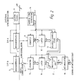
- the correlator 1 of Figure 1 is shown to be correlating two signals S1, S2 formed by e.g. light flux from light scattering experiments.
- the light is detected by photomultipliers PM1, PM2 and fed into derandomisers 2, 3.
- derandomisers 2, 3. For most light experiments only a single light flux is received and an autocorrelation function is to be calculated. In this case only one photomultiplier PM1 is used.
- Output from each photomultipliers 2, 3 is a stream of pulses representing detection of photons in a light flux. These pulses have a random distribution of amplitude and charge.
- the function of each derandomiser 2, 3 is to take the output of the photomultiplier, or any other similar signal, and procedure a pulse of uniform height and with for each photon detected. Two such consecutive pulses will have a minimum separation set by the dead times of the derandomisers 2, 3. Additionally each pulse is synchronised to a basic system clock 9. This allows the subsequent processing to be unambiguous. The result is a train of pulses of varying spacing in time as shown for example in Figure 4(a).
- Outputs from the derandomisers 2, 3 are taken to each channel 41 to 4 M of the correlator.
- a readout circuit 5 receives data from each channel and feeds signals to a controlling logic system, e.g. a digital computer 6, to a CRT display 7, and a recording unit such as a disc or tape store 8.
- the system clock 9 provides a fundamental frequency for all elements of the correlator; typically the frequency is about 100 MHz.
- avalanche photo diodes APD may be used and operated in the geiger mode.
- the correlator layout of Figure 1 is common to many correlators.
- the correlator of the present invention is distinguished by the construction, function and interrelation of each channel as shown in Figure 2.
- Output from the first derandomiser 2 is fed into a counter 11 which counts the number of pulses received in each sample time. The count number is fed via a latch 12 into a delayed sample store 13. Similarly the output of the second derandomiser 3 is fed through a switch 14 into a counter 15.
- the switch 14 also has an input from the first derandomiser 2 and can be set to receive signals from the second derandomiser 3 when a cross correlation is required, or set to receive signals from the first derandomiser 2 when an auto correlation is required.
- the counter 15 output is fed through a latch 16 into a immediate input 10 of a multiplier 17.
- a second, delayed, input DD to the multiplier 17 is from the delayed sample store 13.
- the output from the multiplier 17 is to an accumulator 18 which accumulates the successive multiplier outputs during an experimental run.
- the collective outputs of all the accumulators 18 represents the correlation function of an input signal and pass into the read out circuit 5 ( Figure 1).
- outputs from both counters 11, 15, latches 12, 16, and store 13 are 8-bit numbers; the multipliers output are 16-bits numbers; and the accumulator output 32-bit numbers.
- the correlator system clock 9 provides timing pulses to a sample time generator 19. This produces two outputs clock signal, STC 1 and STC2, which clock the counters 11, 15, latches 12, 16 delayed sample store 13 and accumulator 18.
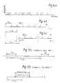
- Figures 4(b), (c) show the timing relation of STC1, STC2 respectively. Both STC1 and STC2 have the same frequency but STC2 is delayed on STC1 by Tm x (N+F); where N is an integer and F is a variable fraction of Tm from zero to just less than unity.
- the effect of STC1 applied to the counter 11 latch 12 and delay store 13 is to sample the incoming signal, Figure 4(a), and form a series of digital numbers each number representing the number of photons received in a sample period Tm.
- the counter 11 counts the number of pulses received between clocking pulses STC1. On receipt of an STC1 pulse the added count is passed into the latch 12 and then into the delay store 13 before the next STC1 pulse.
- the sample period Tm in channel m is set by the frequency of STC1 and can be set at a different value in each channel.
- the counter 11 Whilst the counter 11 is receiving pulses as above the counter 15 is also receiving pulses from the derandomiser 2 or 3, in sample periods set by the STC2 pulses. However, since the start of STC2 is delayed on STC1 the series of digital numbers from latch 16 are delayed on those first written into the delay store 13 by a delay time Tm(M + F).
- the delay store 13 is a FIFO, first in-first out, register. Numbers are clocked in by STC1 and clocked out by STC2. This means that the numbers clocked into the mutliplier 17 from the delay store 13, are delayed data DD, which are multiplied with non-delayed, i.e. immediate dat ID, from the latch 16. Output from the multiplier 17 is thus a series of numbers formed by multiplication of delayed and non-delayed data numbers. Before STC2 begins the outputs of store 13 at latch 16 are zero.
- the switch 14 is set to connect the derandomiser 2 both counters 11, 15.
- Light from a scattering experiment e.g. velocity and turbulence measurements in a wind tunnel, are directed at the photomultiplier PM1.
- the result is a stream of pulses from the derandomiser 2 as in Figure 4(a).
- the train of pulses is divided into sample times Tm set by the STC1 and STC2 clocks, and the number of pulses received in each sample time is counted in both counters 11, 15.
- Delayed data DD from the delay store 13 and non-delayed data ID from the latch 16 are multiplied in the multiplied 17, and result in a series of digital numbers that are accumulated in accumulator 18.
- the contents of each accumulator 18 are read out and normalised.
- the collective normalised value from each channel is the auto correlation function for the input signal S1.
- Tm and delay ⁇ m are variable in each channel.
- the values selected depend on the nature of the experiment being conducted and the accuracy of correlation required.
- Figures 5(a), (b) helps explain the values of delay ⁇ .
- Figure 5(a) shows two equal time periods of length Tm separated by a time delay ⁇ m.
- the value of Tm is the sample time in channel m and varies with each channel in accordance with the frequency of its sample time generator outputs STC1, STC2.
- the value of ⁇ m is equal to Tx(N+F) and can be varied in each channel as required.
- a measure of how much useful information is gathered during a correlation measurement can be obtained by considering the concept of tau space.
- Fig 5b shows the coverage in tau space of any m channel. The coverage in each channel ⁇ c(m) equals twice Tm, and the position of such coverage is ⁇ m.
- GB 84 31,837 introduces the terms ⁇ , ⁇ to describe different sample times and delays in each channel.
- T(m) ⁇ T (m-1)
- T(m) ⁇ (m-1) .T(1)
- alpha, ⁇ is an integer or non integer with alpha (m-1) rounded to the nearest integer.
- ⁇ (m) ⁇ .T(m) where beta, ⁇ is an integer.
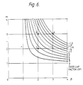
- Figure 7 shows the cover in tau space of GB 1,290,336 for a total of 49 channels.
- the tau coverage is represented by horizontal bars with an associated channel number; the vertical separation is merely to distinguish between channels.
- the value of alpha is 1 and that of beta is m the channel number. This is achieved by passing a signal into a serial delay and taking the output of sucessive stages to one input of multipliers. Non delayed signals go direct to a second input of the multipliers.
- the correlator of the present invention is multibit and can therefore correlate multibit input streams whereas GB 1,290,336 only operates on a single bit values.
- GB 2,115,192 describes a correlator having a variable time delay, tau, between channel.
- Figure 10 shows the coverage of tau space by 14 channels for the illustrate embodiment. There are considerable gaps particularly above the seventh channel.
- Eu 35308943.1 describes a system in which the sample time increases in successive channels.
- the present correlator is capable of calculating correlation functions over tau space coverage not possible with the prior art correlators.
- the present correlator is flexible, i.e. it can be set to operate as any one of the prior art correlators and also in new ways by varying the frequency of and delay between STC1 and STC 2.
- Figure 3 is an alternative to the system of Figure 2. Many components are the same and are given like reference numerals. In Figure 3 there is no multiplier as such; instead a fast adder 21 is employed. As before for auto correlation the output of a derandomiser 2 is fed into a counter 11 to provide numbers in a sample time Tm set by the STC1. From the counter 11 8-bit numbers pass through a latch 12 and into a delayed sample store 13 both clocked by STC1. Output from the delay 13 is timed by STC2 as in Figure 2. Delayed signals DD pass to one terminal of the adder 21.
- Signals from the derandomiser 2, or 3 are fed to a latch 22 Output from this latch 22 is to both the adder 21 and to the readout circuit 5 Figure 1.
- the adder 21 has a sum output to the latch and a carry output to a counter 23. Output from this counter 23 forms the upper 24-bit number that combines with output from the latch 22 forming the lower 8-bit number of a 32-bit number representing the channel correlation coefficient.
- This combination of adder 21 latch 22 and counter 23 performs a multiplication on pulses received in each sample time Tm. This means the components have to be fast enough to act on pulses spaced typically 50 nanosecs apart. For example if the delayed data is 4 and the none delayed data is 3 then: firstly the value 4 will appear at the adder from the delay 13. Each of the three separately received pulses to latch 22 will clock the value 4 round the adder 21 and latch 22 loop three times resulting in a final output of 12.
- An advantage of the Figure 3 system is the reduced number of components. In some cases this reduces the cost.
- the combination of adder 21 latch 22 and counter 23 forms an accumulator and can be used to form the accumulator 18 of Figure 2.
- the latch 22 is clocked by STC 2 instead of a derandomiser output.
- the correlator of Figure 1 is decribed as a multichannel correlator.
- the channel shown in Figures 2, 3 can be used to form single channel correlators.
- a correlation can be performed on a signal with one set of alpha and beta values, and then repeated with different alpha, beta values to cover the required tau space. This may be termed multiplexing and is useful on steady signals or those that change only slowly.
- a two channel correlator may be used, one channel kept with set values of T(m), ⁇ (m), and the other channel multiplexed with different T(m), ⁇ (m) values. This could be useful for example where a spike is expected in a correlation function.
- the set channel provides a background reading value and the variable channel moved around in tau space until the spike is detected.
Landscapes
- Engineering & Computer Science (AREA)
- Physics & Mathematics (AREA)
- General Physics & Mathematics (AREA)
- Mathematical Physics (AREA)
- Computational Mathematics (AREA)
- Mathematical Analysis (AREA)
- Mathematical Optimization (AREA)
- Pure & Applied Mathematics (AREA)
- Theoretical Computer Science (AREA)
- Data Mining & Analysis (AREA)
- Software Systems (AREA)
- Databases & Information Systems (AREA)
- Computing Systems (AREA)
- General Engineering & Computer Science (AREA)
- Algebra (AREA)
- Radar Systems Or Details Thereof (AREA)
- Electrophonic Musical Instruments (AREA)
- Oscillators With Electromechanical Resonators (AREA)
- Photoreceptors In Electrophotography (AREA)
- Complex Calculations (AREA)
- Synchronisation In Digital Transmission Systems (AREA)
- Circuits Of Receivers In General (AREA)
Priority Applications (1)
| Application Number | Priority Date | Filing Date | Title |
|---|---|---|---|
| AT87907616T ATE78352T1 (de) | 1986-11-27 | 1987-11-26 | Digitaler korrelator. |
Applications Claiming Priority (2)
| Application Number | Priority Date | Filing Date | Title |
|---|---|---|---|
| GB8628397 | 1986-11-27 | ||
| GB868628397A GB8628397D0 (en) | 1986-11-27 | 1986-11-27 | Digital correlator/structurator |
Publications (2)
| Publication Number | Publication Date |
|---|---|
| EP0333732A1 EP0333732A1 (en) | 1989-09-27 |
| EP0333732B1 true EP0333732B1 (en) | 1992-07-15 |
Family
ID=10608054
Family Applications (1)
| Application Number | Title | Priority Date | Filing Date |
|---|---|---|---|
| EP87907616A Expired EP0333732B1 (en) | 1986-11-27 | 1987-11-26 | Digital correlator |
Country Status (7)
| Country | Link |
|---|---|
| US (1) | US5020015A (ja) |
| EP (1) | EP0333732B1 (ja) |
| JP (1) | JPH0833882B2 (ja) |
| AT (1) | ATE78352T1 (ja) |
| DE (1) | DE3780469T2 (ja) |
| GB (1) | GB8628397D0 (ja) |
| WO (1) | WO1988004079A1 (ja) |
Families Citing this family (8)
| Publication number | Priority date | Publication date | Assignee | Title |
|---|---|---|---|---|
| US4937775A (en) * | 1988-11-21 | 1990-06-26 | General Electric Company | Apparatus for the cross-correlation of a pair of complex sampled signals |
| CA2166247A1 (en) * | 1995-12-28 | 1997-06-29 | Ravi Shankar Ananth | Supervisory circuit |
| KR100204564B1 (ko) * | 1996-12-09 | 1999-06-15 | 정선종 | 업/다운 계수기를 이용한 고속 상관기 |
| RU2128847C1 (ru) * | 1997-09-11 | 1999-04-10 | Канарейкин Дмитрий Борисович | Устройство для определения состояния атмосферы |
| FR2810108B1 (fr) | 2000-06-09 | 2004-04-02 | France Telecom | Ellipsometre spectroscopique a faible bruit |
| WO2010113926A1 (ja) * | 2009-03-31 | 2010-10-07 | 日本電気株式会社 | 測定装置、測定システム、測定方法、及びプログラム |
| US9602228B1 (en) | 2013-01-18 | 2017-03-21 | Gregory R. Warnes | Method and apparatus for transmission and reception of a signal over multiple frequencies with time offset encoding at each frequency |
| CN111208772B (zh) * | 2020-03-04 | 2025-08-15 | 明峰医疗系统股份有限公司 | 可减少adc通道且不丢失多击中事例的开关选择电路 |
Family Cites Families (7)
| Publication number | Priority date | Publication date | Assignee | Title |
|---|---|---|---|---|
| US3878381A (en) * | 1966-12-07 | 1975-04-15 | Us Navy | Correlation circuit including vernier |
| US3842252A (en) * | 1969-03-26 | 1974-10-15 | Nat Res Dev | Optical signal processing |
| US4404645A (en) * | 1980-08-18 | 1983-09-13 | Elings Virgil B | Correlator |
| DE3381326D1 (de) * | 1982-02-15 | 1990-04-19 | Secr Defence Brit | Digitales signalverarbeitungsgeraet. |
| US4559607A (en) * | 1983-07-11 | 1985-12-17 | International Telephone And Telegraph Corporation | Arrangement to provide an accurate time-of-arrival indication for a plurality of received signals |
| GB8431837D0 (en) * | 1984-12-17 | 1985-01-30 | Secr Defence | Digital signal processor |
| DE3633769A1 (de) * | 1986-10-03 | 1988-04-14 | Endress Hauser Gmbh Co | Digitaler korrelator |
-
1986
- 1986-11-27 GB GB868628397A patent/GB8628397D0/en active Pending
-
1987
- 1987-11-26 US US07/359,755 patent/US5020015A/en not_active Expired - Lifetime
- 1987-11-26 AT AT87907616T patent/ATE78352T1/de not_active IP Right Cessation
- 1987-11-26 EP EP87907616A patent/EP0333732B1/en not_active Expired
- 1987-11-26 DE DE8787907616T patent/DE3780469T2/de not_active Expired - Fee Related
- 1987-11-26 WO PCT/GB1987/000845 patent/WO1988004079A1/en not_active Ceased
- 1987-11-26 JP JP62507100A patent/JPH0833882B2/ja not_active Expired - Fee Related
Also Published As
| Publication number | Publication date |
|---|---|
| DE3780469T2 (de) | 1993-03-04 |
| ATE78352T1 (de) | 1992-08-15 |
| EP0333732A1 (en) | 1989-09-27 |
| GB8628397D0 (en) | 1986-12-31 |
| JPH0833882B2 (ja) | 1996-03-29 |
| DE3780469D1 (de) | 1992-08-20 |
| WO1988004079A1 (en) | 1988-06-02 |
| JPH02500782A (ja) | 1990-03-15 |
| US5020015A (en) | 1991-05-28 |
Similar Documents
| Publication | Publication Date | Title |
|---|---|---|
| US4593378A (en) | Digital signal processor | |
| US7065473B2 (en) | Method and apparatus for improving resolution in spectrometers processing output steps from non-ideal signal sources | |
| US6369393B1 (en) | Digital pulse de-randomization for radiation spectroscopy | |
| EP0333732B1 (en) | Digital correlator | |
| Jordanov et al. | Digital pulse processor using moving average technique | |
| JP2011511927A (ja) | デジタルパルスプロセッサの傾き補正 | |
| Warburton et al. | New algorithms for improved digital pulse arrival timing with sub-GSps ADCs | |
| US5369606A (en) | Reduced state fir filter | |
| US4404645A (en) | Correlator | |
| Ables et al. | A 1024− channel digital correlator | |
| US3842252A (en) | Optical signal processing | |
| EP1206832A1 (en) | Method and apparatus for improving resolution in spectrometers processing output steps from non-ideal signal sources | |
| EP0186987B1 (en) | Digital signal processor | |
| US4884229A (en) | Method and apparatus for removing noise | |
| US4969095A (en) | Scintillation camera having computer control of electrical signals indicating scintillations | |
| EP0425095A1 (en) | Method and apparatus for frequency measurement | |
| CN1963551A (zh) | 用于周期性采样的高分辨率时间戳 | |
| Kasagi et al. | Use of charge integrating ADCs with pulse shape discriminators for neutron-gamma discrimination | |
| Bordessoule et al. | Highly integrated pulse processor | |
| SU703826A1 (ru) | Многоканальный цифровой фильтр | |
| SU1149277A1 (ru) | Цифровой автокоррел тор | |
| SU1506562A1 (ru) | Устройство дл измерени отношени сигнал-шум в радиоприемнике | |
| GB2161301A (en) | Cross-correlator | |
| Lehto et al. | A polarity-correlation system for fast-reactor noise studies | |
| SU702339A1 (ru) | Цифровой измеритель дисперсионных характеристик линий задержки |
Legal Events
| Date | Code | Title | Description |
|---|---|---|---|
| PUAI | Public reference made under article 153(3) epc to a published international application that has entered the european phase |
Free format text: ORIGINAL CODE: 0009012 |
|
| 17P | Request for examination filed |
Effective date: 19890420 |
|
| AK | Designated contracting states |
Kind code of ref document: A1 Designated state(s): AT BE CH DE FR GB IT LI LU NL SE |
|
| 17Q | First examination report despatched |
Effective date: 19910227 |
|
| GRAA | (expected) grant |
Free format text: ORIGINAL CODE: 0009210 |
|
| ITF | It: translation for a ep patent filed | ||
| AK | Designated contracting states |
Kind code of ref document: B1 Designated state(s): AT BE CH DE FR GB IT LI LU NL SE |
|
| REF | Corresponds to: |
Ref document number: 78352 Country of ref document: AT Date of ref document: 19920815 Kind code of ref document: T |
|
| ET | Fr: translation filed | ||
| REF | Corresponds to: |
Ref document number: 3780469 Country of ref document: DE Date of ref document: 19920820 |
|
| PLBE | No opposition filed within time limit |
Free format text: ORIGINAL CODE: 0009261 |
|
| STAA | Information on the status of an ep patent application or granted ep patent |
Free format text: STATUS: NO OPPOSITION FILED WITHIN TIME LIMIT |
|
| 26N | No opposition filed | ||
| EPTA | Lu: last paid annual fee | ||
| EAL | Se: european patent in force in sweden |
Ref document number: 87907616.4 |
|
| REG | Reference to a national code |
Ref country code: GB Ref legal event code: 732E |
|
| BECA | Be: change of holder's address |
Free format text: 20011123 *QINETIQ LTD:85 BUCKINGHAM GATE, LONDON SW14 0LX |
|
| REG | Reference to a national code |
Ref country code: GB Ref legal event code: IF02 |
|
| REG | Reference to a national code |
Ref country code: FR Ref legal event code: TP |
|
| NLS | Nl: assignments of ep-patents |
Owner name: QINETIQ LIMITED |
|
| PGFP | Annual fee paid to national office [announced via postgrant information from national office to epo] |
Ref country code: AT Payment date: 20021008 Year of fee payment: 16 |
|
| PGFP | Annual fee paid to national office [announced via postgrant information from national office to epo] |
Ref country code: FR Payment date: 20021010 Year of fee payment: 16 |
|
| PGFP | Annual fee paid to national office [announced via postgrant information from national office to epo] |
Ref country code: GB Payment date: 20021016 Year of fee payment: 16 |
|
| PGFP | Annual fee paid to national office [announced via postgrant information from national office to epo] |
Ref country code: CH Payment date: 20021018 Year of fee payment: 16 |
|
| PGFP | Annual fee paid to national office [announced via postgrant information from national office to epo] |
Ref country code: NL Payment date: 20021021 Year of fee payment: 16 |
|
| PGFP | Annual fee paid to national office [announced via postgrant information from national office to epo] |
Ref country code: SE Payment date: 20021022 Year of fee payment: 16 Ref country code: DE Payment date: 20021022 Year of fee payment: 16 |
|
| PGFP | Annual fee paid to national office [announced via postgrant information from national office to epo] |
Ref country code: LU Payment date: 20021024 Year of fee payment: 16 |
|
| PGFP | Annual fee paid to national office [announced via postgrant information from national office to epo] |
Ref country code: BE Payment date: 20021122 Year of fee payment: 16 |
|
| PG25 | Lapsed in a contracting state [announced via postgrant information from national office to epo] |
Ref country code: LU Free format text: LAPSE BECAUSE OF NON-PAYMENT OF DUE FEES Effective date: 20031126 Ref country code: GB Free format text: LAPSE BECAUSE OF NON-PAYMENT OF DUE FEES Effective date: 20031126 Ref country code: AT Free format text: LAPSE BECAUSE OF NON-PAYMENT OF DUE FEES Effective date: 20031126 |
|
| PG25 | Lapsed in a contracting state [announced via postgrant information from national office to epo] |
Ref country code: SE Free format text: LAPSE BECAUSE OF NON-PAYMENT OF DUE FEES Effective date: 20031127 |
|
| PG25 | Lapsed in a contracting state [announced via postgrant information from national office to epo] |
Ref country code: LI Free format text: LAPSE BECAUSE OF NON-PAYMENT OF DUE FEES Effective date: 20031130 Ref country code: CH Free format text: LAPSE BECAUSE OF NON-PAYMENT OF DUE FEES Effective date: 20031130 Ref country code: BE Free format text: LAPSE BECAUSE OF NON-PAYMENT OF DUE FEES Effective date: 20031130 |
|
| BERE | Be: lapsed |
Owner name: *QINETIQ LTD Effective date: 20031130 |
|
| PG25 | Lapsed in a contracting state [announced via postgrant information from national office to epo] |
Ref country code: NL Free format text: LAPSE BECAUSE OF NON-PAYMENT OF DUE FEES Effective date: 20040601 |
|
| PG25 | Lapsed in a contracting state [announced via postgrant information from national office to epo] |
Ref country code: DE Free format text: LAPSE BECAUSE OF NON-PAYMENT OF DUE FEES Effective date: 20040602 |
|
| EUG | Se: european patent has lapsed | ||
| GBPC | Gb: european patent ceased through non-payment of renewal fee |
Effective date: 20031126 |
|
| REG | Reference to a national code |
Ref country code: CH Ref legal event code: PL |
|
| PG25 | Lapsed in a contracting state [announced via postgrant information from national office to epo] |
Ref country code: FR Free format text: LAPSE BECAUSE OF NON-PAYMENT OF DUE FEES Effective date: 20040730 |
|
| NLV4 | Nl: lapsed or anulled due to non-payment of the annual fee |
Effective date: 20040601 |
|
| REG | Reference to a national code |
Ref country code: FR Ref legal event code: ST |
|
| PG25 | Lapsed in a contracting state [announced via postgrant information from national office to epo] |
Ref country code: IT Free format text: LAPSE BECAUSE OF NON-PAYMENT OF DUE FEES;WARNING: LAPSES OF ITALIAN PATENTS WITH EFFECTIVE DATE BEFORE 2007 MAY HAVE OCCURRED AT ANY TIME BEFORE 2007. THE CORRECT EFFECTIVE DATE MAY BE DIFFERENT FROM THE ONE RECORDED. Effective date: 20051126 |