EP0332135B1 - Nonvolatile memory circuit device with low power consumption and wide operating voltage range - Google Patents
Nonvolatile memory circuit device with low power consumption and wide operating voltage range Download PDFInfo
- Publication number
- EP0332135B1 EP0332135B1 EP89103991A EP89103991A EP0332135B1 EP 0332135 B1 EP0332135 B1 EP 0332135B1 EP 89103991 A EP89103991 A EP 89103991A EP 89103991 A EP89103991 A EP 89103991A EP 0332135 B1 EP0332135 B1 EP 0332135B1
- Authority
- EP
- European Patent Office
- Prior art keywords
- potential
- node
- transistor
- circuit
- vcc
- Prior art date
- Legal status (The legal status is an assumption and is not a legal conclusion. Google has not performed a legal analysis and makes no representation as to the accuracy of the status listed.)
- Expired - Lifetime
Links
Images


Classifications
-
- G—PHYSICS
- G11—INFORMATION STORAGE
- G11C—STATIC STORES
- G11C11/00—Digital stores characterised by the use of particular electric or magnetic storage elements; Storage elements therefor
-
- G—PHYSICS
- G11—INFORMATION STORAGE
- G11C—STATIC STORES
- G11C16/00—Erasable programmable read-only memories
- G11C16/02—Erasable programmable read-only memories electrically programmable
- G11C16/06—Auxiliary circuits, e.g. for writing into memory
- G11C16/26—Sensing or reading circuits; Data output circuits
- G11C16/28—Sensing or reading circuits; Data output circuits using differential sensing or reference cells, e.g. dummy cells
Definitions
- This invention relates to a nonvolatile memory circuit device having nonvolatile transistors as memory cells as indicated in the preamble of Claim 1.
- a circuit device is discussed in IEEE Journal of solid-state circuits, Vol. SC-22, No. 5, Oct. 1987 at pp 669-675.
- the memory cells of the nonvolatile memory circuit device have been miniaturized, it becomes highly possible that the memory cell will be damaged or data will be erroneously programmed when a power source voltage is applied to the drain of the memory cell as it is in the data readout mode. For this reason, it is required to suppress the drain voltage of the memory cell to a certain low voltage level during the data readout mode of the memory circuit of this type, and at the same time it is necessary to attain the highly reliable readout operation.
- Fig. 1 is a circuit diagram showing the circuit construction of the conventional nonvolatile memory circuit device. For clarifying the explanation, a data writing or programming circuit and the related circuits are omitted.
- intermediate potential output circuit 30 for supplying a potential lower than potential Vcc is connected between positive power source potential terminal Vcc and node A.
- a plurality of column selection transistors 31 are commonly connected at one end to node A and respectively connected at the other end to bit lines 32.
- a plurality of word lines 33 are arranged to intersect bit lines 32, and memory cells 34 formed of nonvolatile transistors are arranged in respective positions in which the bit lines and word lines intersect each other.
- drains of those memory cells which lie on the same column are connected to a corresponding one of bit lines 32 and the gates of those memory cells which lie on the same row are connected to a corresponding one of word lines 33.
- the sources of the memory cells are connected to ground potential terminal Vss.
- sense amplifier 35 formed of a voltage comparator having an analog circuit structure is connected to node A.
- Reference potential Vref which is slightly lower than the output potential of intermediate potential output circuit 30 is supplied to sense amplifier 35 which in turn compares the potential at node A with reference potential Vref to output data Dout corresponding to the comparison result.
- the potential at node A is always kept at a potential level lower than power source potential Vcc by means of intermediate potential output circuit 30.
- the lower potential is supplied to the drain of a memory cell selected in the data readout mode, and therefore the above-described problems of damage of the memory cell and erroneous programming operation can be solved.
- the amplitude of potential at node A is limited by the presence of intermediate potential output circuit 30, and it is required to use a voltage comparator type sense amplifier with complicated analog circuit construction as sense amplifier 35.
- Such a sense amplifier has disadvantages that the power source voltage margin is reduced, a low voltage operation is difficult and the current consumption is large.
- intermediate potential output circuit 30 is required to have a large current capacity and consequently the circuit construction thereof becomes complex.
- the potential to be detected by the sense amplifier is set at a low level to prevent damage of the memory cell and erroneous programming operation, there arise problems that it cannot be driven at a low voltage and the current consumption becomes large.
- This invention has been made based on the above-described fact, and an object of this invention is to provide a nonvolatile memory circuit device which can be operated at a low voltage and has a reduced current consumption without lowering the operation reliability in the readout mode.
- a nonvolatile memory circuit device which comprises a memory cell array having a plurality of memory cells formed of nonvolatile transistors; a plurality of column lines connected to the drains of the memory cells; a plurality of column selection transistors respectively connected at one end to the column lines and commonly connected at the other end to a first node; a precharging transistor of a first conductivity type connected between a first potential terminal and the first node; a discharging transistor of a second conductivity type connected between a second potential terminal and the sources of the memory cells; a potential supplying circuit for selectively supplying a potential lower than the first potential at the first potential terminal to the gates of the column selection transistors according to address input; and a sense amplifier connected to the first node.
- a potential lower than the power source potential is supplied to the gates of the column selection transistors to suppress the drain potential of the memory cells to a low potential level.
- the potential supplying circuit for supplying the gate potential to the column selection transistors is used only to charge the gate capacity of the column selection transistors, and therefore the current capacity thereof can be reduced and the construction thereof can be simplified.
- the first node to which the sense amplifier is connected is precharged to the power source potential by means of the precharging transistor, and the sources of the memory cells are discharged by means of the discharging transistor when a memory cell is selected. Therefore, no D.C. penetration current will flow and the current consumption can be reduced.
- the first node to which the sense amplifier is connected is precharged to the first potential which is the power source potential, the amplitude of potential at the first node can be made sufficiently large.
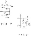
- Fig. 2 is a circuit diagram showing the construction of a nonvolatile memory circuit device according to one embodiment of this invention. For clarifying the explanation, a programming circuit and the associated circuits are omitted.
- precharging transistor 1 formed of a P-channel MOS transistor is connected between positive power source potential terminal Vss and data detection node or node A.
- Precharging signal Pr is supplied to the gate of transistor 1.
- a plurality of column selection transistors 2 formed of N-channel MOS transistors are commonly connected at one end to node A, and are respectively connected at the other end to bit lines 3.
- a plurality of word lines 4 are arranged to intersect bit lines 3. Word lines 4 are selectively driven by the output of row decoder 5.
- memory cells 6 formed of nonvolatile transistors having the floating gate structure are arranged in respective positions in which bit lines 3 and word lines 4 intersect.
- the drains of those of the memory cells which lie on the same column are connected to a corresponding one of bit lines 3 and the gates of those memory cells which lie on the same row are connected to a corresponding one of word lines 4.
- the sources of memory cells 6 are commonly connected to the drain of discharging transistor 7 formed of an N-channel MOS transistor.
- the source of discharging transistor 7 is connected to ground potential terminal Vss.
- Constant potential VDD which is lower than power source potential Vcc and higher than ground potential Vss is supplied from intermediate potential generating circuit 8.
- Potential VDD is supplied to column decoder 9 to which a column address signal is also supplied.
- Column decoder 9 selectively supplies potential VDD to the gates of column selection transistors 2 according to the received column address signal.
- Sense amplifier 10 is connected node A.
- Sense amplifier 10 is constituted by a flip-flop circuit including two CMOS NOR gate circuits 11 and 12 whose input and output terminals are cross-coupled.
- the potential at node A is supplied to NOR gate circuit 11 and comparison voltage Vref generated from reference potential generating circuit 13 is supplied to NOR gate circuit 12.
- Reference potential generating circuit 13 includes transistor 14 which is formed to be equivalent to column selection transistor 2 and whose gate is supplied with a potential equal to constant potential VDD in the memory cell selecting operation, transistor 15 which is formed to be equivalent to precharging transistor 1 and whose gate is supplied with precharge signal Pr, dummy cell 16 having a similar nonvolatile transistor structure to that of memory cell 6 and formed to have a source-drain current half that of memory cell 6, and transistor 17 connected between dummy cell 16 and ground potential terminal Vss, formed to be equivalent to discharging transistor 1, and having a gate supplied with precharging signal Pr.
- precharge signal Pr is set to "L” level to turn on precharging transistor 1 after readout control signal Rd is set to and kept at "H” level.
- node A is precharged to power source potential Vcc (precharging period Tp).
- discharging transistor 7 is turned off to prevent a D.C. penetration current from flowing between power source potential terminal Vcc and ground potential terminal Vss.
- transistors 15 and 17 of reference potential generating circuit 13 are respectively turned on and off, thereby causing node B connected to sense amplifier 10 to be precharged to Vcc level. Since, in this case, both nodes A and B are precharged to Vcc level or "H” level, output data Dout of sense amplifier 10 is set to "L" level.
- precharge signal Pr is changed form "L" to "H” level.
- Precharge signal Pr of "H” level renders transistor 7 conductive to start the data readout period (discharging period Td). Turn-on of transistor 7 causes the sources of memory cells 6 to be set to the ground potential.
- one of column selection transistors 2 is selected by column decoder 9 according to the column address signal, and constant potential VDD from intermediate potential generating circuit 8 is supplied to the gate of selected transistor 2. As the result of this, selected transistor 2 is turned on.
- the selected memory cell Assuming now that the selected memory cell has been programmed to have a lower threshold voltage, then the selected memory cell is turned on and bit line 3 and node A are discharged to ground potential Vss. In contrast, if the selected memory cell has been programmed to have a higher threshold voltage, the selected memory cell is turned off and neither bit line 3 nor node A is discharged.
- precharge signal Pr When precharge signal Pr is changed from “L” level to “H” level, transistor 17 of reference potential generating circuit 13 is turned on. Further, when one of column selection transistors 2 is selected, intermediate potential VDD is supplied to the gate of transistor 14. As a result, node B is discharged from power source potential level Vcc. Assume now that the threshold voltage of selected memory cell 6 is low and node A is also discharged. Then, since the source-drain current of dummy cell 16 of reference potential generating circuit 13 is set to be substantially half that of memory cell 6, the potential at node A approaches Vss more rapidly than that at node B. As a result, output data Dout of sense amplifier 10 is inverted from “L" level to "H” level. In contrast, if the threshold voltage of selected memory cell 6 is high, node A is not discharged and node B is discharged so that output data Dout will be kept unchanged and remain at "L” level. In this way, data can be read out from the selected memory cell.
- Node A is precharged to the power source potential via transistor 1 in the data readout period, and then the source of each memory cell 6 is discharged to the ground potential via transistor 7 so that a D.C. penetration current can be prevented from flowing between the power source potential terminal and the ground potential terminal. Thus, the current consumption can be reduced.
- intermediate potential generating circuit 8 for generating a potential lower than the power source potential is required only to drive the gate of column selection transistor 2, the current capacity thereof can be made small, the current consumption can be reduced and the construction can be simplified.
- sense amplifier 10 can be formed of a logic gate circuit which is constructed by NOR gate circuits 11 and 12 in a simple construction as shown in Fig. 2, and thus the current consumption can be reduced. In this case, if NOR gate circuits 11 and 12 are formed in the CMOS form, the current consumption can be further reduced.
- the use of the logic circuit which is constructed in a flip-flop form makes it possible to attain the stable circuit operation over a wide voltage range, the low power consumption and the low voltage operation.
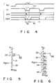
- Figs. 5, 6 and 7 are circuit diagrams showing the detail construction of intermediate potential generating circuit 8 which can be used in the circuit of the above embodiment.
- P-channel MOS transistor or switching transistor 20 and two resistors 21 and 22 are serially connected between power source potential terminal Vcc and ground potential terminal Vss.
- the conduction state of switching transistor 20 is controlled by, for example, signal Rd which takes an inverted form of readout control signal Rd and is set to "L" level in the data readout mode.
- signal Rd which takes an inverted form of readout control signal Rd and is set to "L" level in the data readout mode.
- transistor 20 With the circuit of Fig. 5, transistor 20 is kept in the off state in a period other than the data readout period, and therefore no current consumption occurs.
- transistor 20 is turned on so that potential VDD which is obtained by dividing potential Vcc by resistors 21 and 22 and is thus lower than potential Vcc can be derived.
- P-channel MOS transistor or switching transistor 23 and a plurality of P-channel MOS transistors 24 are serially connected between power source potential terminal Vcc and ground potential terminal Vss.
- the conduction state of switching transistor 23 is controlled by signal Rd.
- transistor 23 is kept in the off state in a period other than the data readout period, and therefore no current consumption occurs.
- transistor 23 is turned on so that potential VDD which is obtained by dividing potential Vcc by the resistances of switching transistor 23 and a plurality of transistors 24 and is thus lower than potential Vcc can be derived.
- N-channel MOS transistor 26 of depletion type and N-channel MOS transistor 27 of intrinsic type are serially connected between power source potential terminal Vcc and ground potential terminal Vss.
- the gates of transistors 26 and 27 and a connection node therebetween are connected together to make output node D and the conduction state of switching transistor 25 is controlled by signal Rd.
- transistor 25 is kept in the off state in a period other than the data readout period, and therefore no current consumption occurs.
- transistor 25 is turned on so that voltage VDD which is obtained by dividing the drain voltage of switching transistor 25 by ON-resistances of transistors 26 and 27 is thus lower than voltage Vcc can be derived out via output node D.
- This invention is not limited to the above-described embodiments, and can be variously modified within the technical scope thereof.
- intermediate potential generating circuit 8 and sense amplifier 10 are not limited to those shown in the drawings, but can be variously modified.
- a nonvolatile memory circuit device can be provided in which the circuit construction can be simplified without lowering the operation reliability in the readout mode and which can be operated at a low voltage and with a small power consumption.
Description
- This invention relates to a nonvolatile memory circuit device having nonvolatile transistors as memory cells as indicated in the preamble of Claim 1. Such a circuit device is discussed in IEEE Journal of solid-state circuits, Vol. SC-22, No. 5, Oct. 1987 at pp 669-675.
- As the memory cells of the nonvolatile memory circuit device have been miniaturized, it becomes highly possible that the memory cell will be damaged or data will be erroneously programmed when a power source voltage is applied to the drain of the memory cell as it is in the data readout mode. For this reason, it is required to suppress the drain voltage of the memory cell to a certain low voltage level during the data readout mode of the memory circuit of this type, and at the same time it is necessary to attain the highly reliable readout operation.
- Fig. 1 is a circuit diagram showing the circuit construction of the conventional nonvolatile memory circuit device. For clarifying the explanation, a data writing or programming circuit and the related circuits are omitted. As shown in Fig. 1, intermediate
potential output circuit 30 for supplying a potential lower than potential Vcc is connected between positive power source potential terminal Vcc and node A. A plurality ofcolumn selection transistors 31 are commonly connected at one end to node A and respectively connected at the other end tobit lines 32. A plurality ofword lines 33 are arranged to intersectbit lines 32, andmemory cells 34 formed of nonvolatile transistors are arranged in respective positions in which the bit lines and word lines intersect each other. The drains of those memory cells which lie on the same column are connected to a corresponding one ofbit lines 32 and the gates of those memory cells which lie on the same row are connected to a corresponding one ofword lines 33. The sources of the memory cells are connected to ground potential terminal Vss. Further,sense amplifier 35 formed of a voltage comparator having an analog circuit structure is connected to node A. Reference potential Vref which is slightly lower than the output potential of intermediatepotential output circuit 30 is supplied to senseamplifier 35 which in turn compares the potential at node A with reference potential Vref to output data Dout corresponding to the comparison result. - With memory circuit of the above construction, the potential at node A is always kept at a potential level lower than power source potential Vcc by means of intermediate
potential output circuit 30. As a result, the lower potential is supplied to the drain of a memory cell selected in the data readout mode, and therefore the above-described problems of damage of the memory cell and erroneous programming operation can be solved. - However, the amplitude of potential at node A is limited by the presence of intermediate
potential output circuit 30, and it is required to use a voltage comparator type sense amplifier with complicated analog circuit construction assense amplifier 35. Such a sense amplifier has disadvantages that the power source voltage margin is reduced, a low voltage operation is difficult and the current consumption is large. - Further, when
memory cell 34 selected in the data readout mode is turned on, a D.C. penetration current flows between power source potential terminal Vcc and ground potential terminal Vss, further increasing the current consumption. In addition, intermediatepotential output circuit 30 is required to have a large current capacity and consequently the circuit construction thereof becomes complex. - As described above, since, in the conventional nonvolatile memory circuit device, the potential to be detected by the sense amplifier is set at a low level to prevent damage of the memory cell and erroneous programming operation, there arise problems that it cannot be driven at a low voltage and the current consumption becomes large.
- This invention has been made based on the above-described fact, and an object of this invention is to provide a nonvolatile memory circuit device which can be operated at a low voltage and has a reduced current consumption without lowering the operation reliability in the readout mode.
- According to the invention, there is provided a nonvolatile memory circuit device which comprises a memory cell array having a plurality of memory cells formed of nonvolatile transistors; a plurality of column lines connected to the drains of the memory cells; a plurality of column selection transistors respectively connected at one end to the column lines and commonly connected at the other end to a first node; a precharging transistor of a first conductivity type connected between a first potential terminal and the first node; a discharging transistor of a second conductivity type connected between a second potential terminal and the sources of the memory cells; a potential supplying circuit for selectively supplying a potential lower than the first potential at the first potential terminal to the gates of the column selection transistors according to address input; and a sense amplifier connected to the first node.
- In the nonvolatile memory circuit device of this invention, a potential lower than the power source potential is supplied to the gates of the column selection transistors to suppress the drain potential of the memory cells to a low potential level. The potential supplying circuit for supplying the gate potential to the column selection transistors is used only to charge the gate capacity of the column selection transistors, and therefore the current capacity thereof can be reduced and the construction thereof can be simplified.
- Further, in the nonvolatile memory circuit device of this invention, the first node to which the sense amplifier is connected is precharged to the power source potential by means of the precharging transistor, and the sources of the memory cells are discharged by means of the discharging transistor when a memory cell is selected. Therefore, no D.C. penetration current will flow and the current consumption can be reduced. In addition, since the first node to which the sense amplifier is connected is precharged to the first potential which is the power source potential, the amplitude of potential at the first node can be made sufficiently large. Thus, it becomes possible to constitute the sense amplifier connected to the first node by use of logic gate circuits. As a result, the power source voltage margin of the sense amplifier can be improved and the current consumption can be reduced.
- This invention can be more fully understood from the following detailed description when taken in conjunction with the accompanying drawings, in which:
- Fig. 1 is a block diagram showing the conventional nonvolatile memory circuit;
- Fig. 2 is a block diagram showing a nonvolatile memory circuit device according to one embodiment of this invention;
- Fig. 3 is a circuit diagram showing a modification of the embodiment of Fig. 2;
- Fig. 4 is a timing chart for illustrating the operation the circuits shown in Figs. 2 and 3; and
- Figs. 5 to 7 are circuit diagrams respectively showing the construction of portions of the circuit of Fig. 2.
- There will now be described an embodiment of this invention with reference to the accompanying drawings.
- Fig. 2 is a circuit diagram showing the construction of a nonvolatile memory circuit device according to one embodiment of this invention. For clarifying the explanation, a programming circuit and the associated circuits are omitted. As shown in Fig. 2, precharging transistor 1 formed of a P-channel MOS transistor is connected between positive power source potential terminal Vss and data detection node or node A. Precharging signal Pr is supplied to the gate of transistor 1. A plurality of
column selection transistors 2 formed of N-channel MOS transistors are commonly connected at one end to node A, and are respectively connected at the other end tobit lines 3. A plurality ofword lines 4 are arranged to intersectbit lines 3.Word lines 4 are selectively driven by the output ofrow decoder 5. Further,memory cells 6 formed of nonvolatile transistors having the floating gate structure are arranged in respective positions in whichbit lines 3 andword lines 4 intersect. The drains of those of the memory cells which lie on the same column are connected to a corresponding one ofbit lines 3 and the gates of those memory cells which lie on the same row are connected to a corresponding one ofword lines 4. The sources ofmemory cells 6 are commonly connected to the drain of dischargingtransistor 7 formed of an N-channel MOS transistor. The source of dischargingtransistor 7 is connected to ground potential terminal Vss. - It is also possible to use an
individual discharging transistor 7 for eachmemory cell 6 in such a manner as shown in Fig. 3. - Constant potential VDD which is lower than power source potential Vcc and higher than ground potential Vss is supplied from intermediate
potential generating circuit 8. Potential VDD is supplied tocolumn decoder 9 to which a column address signal is also supplied.Column decoder 9 selectively supplies potential VDD to the gates ofcolumn selection transistors 2 according to the received column address signal. -
Sense amplifier 10 is connected node A. Senseamplifier 10 is constituted by a flip-flop circuit including two CMOSNOR gate circuits NOR gate circuit 11 and comparison voltage Vref generated from referencepotential generating circuit 13 is supplied toNOR gate circuit 12. - Reference
potential generating circuit 13 includestransistor 14 which is formed to be equivalent tocolumn selection transistor 2 and whose gate is supplied with a potential equal to constant potential VDD in the memory cell selecting operation,transistor 15 which is formed to be equivalent to precharging transistor 1 and whose gate is supplied with precharge signal Pr,dummy cell 16 having a similar nonvolatile transistor structure to that ofmemory cell 6 and formed to have a source-drain current half that ofmemory cell 6, andtransistor 17 connected betweendummy cell 16 and ground potential terminal Vss, formed to be equivalent to discharging transistor 1, and having a gate supplied with precharging signal Pr. - Now, the data readout operation in the memory circuit of the above-described construction is explained with reference to the timing chart shown in Fig. 4 First, precharge signal Pr is set to "L" level to turn on precharging transistor 1 after readout control signal Rd is set to and kept at "H" level. As a result, node A is precharged to power source potential Vcc (precharging period Tp). At this time, discharging
transistor 7 is turned off to prevent a D.C. penetration current from flowing between power source potential terminal Vcc and ground potential terminal Vss. Further,transistors circuit 13 are respectively turned on and off, thereby causing node B connected tosense amplifier 10 to be precharged to Vcc level. Since, in this case, both nodes A and B are precharged to Vcc level or "H" level, output data Dout ofsense amplifier 10 is set to "L" level. - Next, column and row addresses ADD are respectively supplied to
column decoder 9 androw decoder 5, and then precharge signal Pr is changed form "L" to "H" level. Precharge signal Pr of "H"level renders transistor 7 conductive to start the data readout period (discharging period Td). Turn-on oftransistor 7 causes the sources ofmemory cells 6 to be set to the ground potential. At the same time, one ofcolumn selection transistors 2 is selected bycolumn decoder 9 according to the column address signal, and constant potential VDD from intermediatepotential generating circuit 8 is supplied to the gate of selectedtransistor 2. As the result of this, selectedtransistor 2 is turned on. However, since the gate potential of selectedtransistor 2 is lower than power source potential Vcc, a potential lower than power source potential Vcc will be supplied to that one ofbit lines 3 which is connected to an activated one ofcolumn selection transistors 2. On the other hand, one ofword lines 4 is selected byrow decoder 5 according to the row address signal. Then, a driving signal of "H" level is supplied to those gates ofmemory cells 6 which are connected to selectedword line 4. As a result, a memory cell lying in the intersecting position between the selected word line and the bit line to which a potential lower than power source potential Vcc is supplied is selected. Assuming now that the selected memory cell has been programmed to have a lower threshold voltage, then the selected memory cell is turned on andbit line 3 and node A are discharged to ground potential Vss. In contrast, if the selected memory cell has been programmed to have a higher threshold voltage, the selected memory cell is turned off and neitherbit line 3 nor node A is discharged. - When precharge signal Pr is changed from "L" level to "H" level,
transistor 17 of referencepotential generating circuit 13 is turned on. Further, when one ofcolumn selection transistors 2 is selected, intermediate potential VDD is supplied to the gate oftransistor 14. As a result, node B is discharged from power source potential level Vcc. Assume now that the threshold voltage of selectedmemory cell 6 is low and node A is also discharged. Then, since the source-drain current ofdummy cell 16 of referencepotential generating circuit 13 is set to be substantially half that ofmemory cell 6, the potential at node A approaches Vss more rapidly than that at node B. As a result, output data Dout ofsense amplifier 10 is inverted from "L" level to "H" level. In contrast, if the threshold voltage of selectedmemory cell 6 is high, node A is not discharged and node B is discharged so that output data Dout will be kept unchanged and remain at "L" level. In this way, data can be read out from the selected memory cell. - Since a potential lower than power source potential Vcc is applied to
bit line 3, damage of the memory cell and erroneous programming operation occurring in the prior art case can be prevented. - Node A is precharged to the power source potential via transistor 1 in the data readout period, and then the source of each
memory cell 6 is discharged to the ground potential viatransistor 7 so that a D.C. penetration current can be prevented from flowing between the power source potential terminal and the ground potential terminal. Thus, the current consumption can be reduced. - Further, since intermediate
potential generating circuit 8 for generating a potential lower than the power source potential is required only to drive the gate ofcolumn selection transistor 2, the current capacity thereof can be made small, the current consumption can be reduced and the construction can be simplified. - In addition, since the potential at node A varies between power source potential Vcc and ground potential Vss,
sense amplifier 10 can be formed of a logic gate circuit which is constructed by NORgate circuits gate circuits - Figs. 5, 6 and 7 are circuit diagrams showing the detail construction of intermediate
potential generating circuit 8 which can be used in the circuit of the above embodiment. - In the circuit of Fig. 5, P-channel MOS transistor or switching
transistor 20 and tworesistors transistor 20 is controlled by, for example, signalRd which takes an inverted form of readout control signal Rd and is set to "L" level in the data readout mode. With the circuit of Fig. 5,transistor 20 is kept in the off state in a period other than the data readout period, and therefore no current consumption occurs. In contrast, in the data readout mode,transistor 20 is turned on so that potential VDD which is obtained by dividing potential Vcc byresistors - In the circuit of Fig. 6, P-channel MOS transistor or switching
transistor 23 and a plurality of P-channel MOS transistors 24 are serially connected between power source potential terminal Vcc and ground potential terminal Vss. In this case, the conduction state of switchingtransistor 23 is controlled by signal Rd. Also, in this circuit,transistor 23 is kept in the off state in a period other than the data readout period, and therefore no current consumption occurs. In contrast, in the data readout mode,transistor 23 is turned on so that potential VDD which is obtained by dividing potential Vcc by the resistances of switchingtransistor 23 and a plurality oftransistors 24 and is thus lower than potential Vcc can be derived. - In the circuit of Fig. 7, P-channel MOS transistor or switching
transistor 25, N-channel MOS transistor 26 of depletion type and N-channel MOS transistor 27 of intrinsic type (having a threshold voltage of about 0 V) are serially connected between power source potential terminal Vcc and ground potential terminal Vss. In this case, the gates oftransistors transistor 25 is controlled by signal Rd. With the circuit of Fig. 7,transistor 25 is kept in the off state in a period other than the data readout period, and therefore no current consumption occurs. In contrast, in the data readout mode,transistor 25 is turned on so that voltage VDD which is obtained by dividing the drain voltage of switchingtransistor 25 by ON-resistances oftransistors transistors - This invention is not limited to the above-described embodiments, and can be variously modified within the technical scope thereof. For example, it is possible to commonly connect the sources of the memory cells to discharging
transistor 7 so that it can be used commonly for all the memory cells connected to one bit line. Further, intermediatepotential generating circuit 8 andsense amplifier 10 are not limited to those shown in the drawings, but can be variously modified. - As described above, according to this invention, a nonvolatile memory circuit device can be provided in which the circuit construction can be simplified without lowering the operation reliability in the readout mode and which can be operated at a low voltage and with a small power consumption.
Claims (3)
- A nonvolatile memory circuit device comprising:
a memory cell array having a plurality of memory cells (6) formed of nonvolatile transistors;
a plurality of column lines (3) connected to drains of said memory cells (6);
a plurality of column selection transistors (2) respectively connected at one end to said column lines (3) and commonly connected at the other end to a first node (A);
a precharging transistor (1) of a first conductivity type connected between a first potential terminal (Vcc) and said first node (A);
at least one discharging transistor (7) of a second conductivity type connected between a second potential terminal (Vss) and sources of said memory cells (6);
a sense amplifier (10) connected to said first node,
characterized by :
potential supplying means (8) for selectively supplying a potential (VDD) lower than the first potential (VCC) at said first potential terminal to gates of said column selection transistors (2) according to address input. - A nonvolatile memory circuit device according to claim 1, characterized in that said sense amplifier (10) includes a flip-flop formed of CMOS logic gate circuit (11, 12) for comparing the potential at said first node (A) with a reference potential (Vref).
- A nonvolatile memory circuit device according to claim 1, characterized in that said device further comprises a power source terminal (Vcc), and said potential supplying means (8) includes a constant potential circuit (25-27) for delivering said potential held at a constant value irrespective of a variation of an output voltage at said power source terminal (Vcc).
Applications Claiming Priority (2)
| Application Number | Priority Date | Filing Date | Title |
|---|---|---|---|
| JP55373/88 | 1988-03-09 | ||
| JP5537388 | 1988-03-09 |
Publications (3)
| Publication Number | Publication Date |
|---|---|
| EP0332135A2 EP0332135A2 (en) | 1989-09-13 |
| EP0332135A3 EP0332135A3 (en) | 1992-03-18 |
| EP0332135B1 true EP0332135B1 (en) | 1994-09-14 |
Family
ID=12996682
Family Applications (1)
| Application Number | Title | Priority Date | Filing Date |
|---|---|---|---|
| EP89103991A Expired - Lifetime EP0332135B1 (en) | 1988-03-09 | 1989-03-07 | Nonvolatile memory circuit device with low power consumption and wide operating voltage range |
Country Status (4)
| Country | Link |
|---|---|
| US (1) | US5001668A (en) |
| EP (1) | EP0332135B1 (en) |
| KR (1) | KR930000963B1 (en) |
| DE (1) | DE68918136T2 (en) |
Families Citing this family (15)
| Publication number | Priority date | Publication date | Assignee | Title |
|---|---|---|---|---|
| US5237534A (en) * | 1989-04-27 | 1993-08-17 | Kabushiki Kaisha Toshiba | Data sense circuit for a semiconductor nonvolatile memory device |
| JP2573380B2 (en) * | 1989-12-22 | 1997-01-22 | 株式会社東芝 | Non-volatile semiconductor memory |
| JPH0426989A (en) * | 1990-05-18 | 1992-01-30 | Toshiba Corp | Dynamic memory device |
| JP2680939B2 (en) * | 1991-03-27 | 1997-11-19 | 日本電気アイシーマイコンシステム株式会社 | Semiconductor memory device |
| JP3313383B2 (en) * | 1991-06-27 | 2002-08-12 | 日本電気株式会社 | Read-only storage device |
| JP2637314B2 (en) * | 1991-08-30 | 1997-08-06 | 株式会社東芝 | Non-volatile memory circuit |
| JP2991546B2 (en) * | 1991-10-07 | 1999-12-20 | 株式会社東芝 | Semiconductor integrated circuit |
| DE4219464A1 (en) * | 1992-06-13 | 1993-12-16 | Philips Patentverwaltung | Method and circuit arrangement for generating a programming voltage |
| US5497475A (en) * | 1993-02-05 | 1996-03-05 | National Semiconductor Corporation | Configurable integrated circuit having true and shadow EPROM registers |
| US6219291B1 (en) * | 2000-05-01 | 2001-04-17 | Advanced Technology Materials, Inc. | Reduction of data dependent power supply noise when sensing the state of a memory cell |
| JP3709132B2 (en) * | 2000-09-20 | 2005-10-19 | シャープ株式会社 | Nonvolatile semiconductor memory device |
| US6424571B1 (en) * | 2001-05-01 | 2002-07-23 | Micron Technology, Inc. | Sense amplifier with data line precharge through a self-bias circuit and a precharge circuit |
| JP3904537B2 (en) * | 2003-07-01 | 2007-04-11 | 沖電気工業株式会社 | Semiconductor memory device |
| US7046566B1 (en) * | 2004-12-06 | 2006-05-16 | Altera Corporation | Voltage-based timing control of memory bit lines |
| US7877058B2 (en) * | 2006-11-10 | 2011-01-25 | Skyworks Solutions, Inc. | Compact low loss high frequency switch with improved linearity performance |
Family Cites Families (13)
| Publication number | Priority date | Publication date | Assignee | Title |
|---|---|---|---|---|
| GB1502270A (en) * | 1974-10-30 | 1978-03-01 | Hitachi Ltd | Word line driver circuit in memory circuit |
| JPS54137933A (en) * | 1978-04-18 | 1979-10-26 | Sharp Corp | Programmable nonvolatile rom |
| US4281397A (en) * | 1979-10-29 | 1981-07-28 | Texas Instruments Incorporated | Virtual ground MOS EPROM or ROM matrix |
| US4314362A (en) * | 1980-02-04 | 1982-02-02 | Texas Instruments, Incorporated | Power down sequence for electrically programmable memory |
| US4394748A (en) * | 1981-08-18 | 1983-07-19 | Motorola, Inc. | ROM Column select circuit and sense amplifier |
| JPS59117787A (en) * | 1982-12-24 | 1984-07-07 | Hitachi Ltd | Eprom device |
| JPS60125998A (en) * | 1983-12-12 | 1985-07-05 | Fujitsu Ltd | Semiconductor storage device |
| JPS60177499A (en) * | 1984-02-22 | 1985-09-11 | Nippon Texas Instr Kk | Serial rom device |
| JPS6173300A (en) * | 1984-09-17 | 1986-04-15 | Toshiba Corp | Semiconductor memory device |
| US4833646A (en) * | 1985-03-04 | 1989-05-23 | Lattice Semiconductor Corp. | Programmable logic device with limited sense currents and noise reduction |
| US4769787A (en) * | 1985-07-26 | 1988-09-06 | Hitachi, Ltd. | Semiconductor memory device |
| JPS6231094A (en) * | 1985-08-01 | 1987-02-10 | Toshiba Corp | Non-volatile semiconductor memory device |
| US4713797A (en) * | 1985-11-25 | 1987-12-15 | Motorola Inc. | Current mirror sense amplifier for a non-volatile memory |
-
1989
- 1989-03-03 KR KR1019890002648A patent/KR930000963B1/en not_active IP Right Cessation
- 1989-03-06 US US07/319,205 patent/US5001668A/en not_active Expired - Lifetime
- 1989-03-07 DE DE68918136T patent/DE68918136T2/en not_active Expired - Fee Related
- 1989-03-07 EP EP89103991A patent/EP0332135B1/en not_active Expired - Lifetime
Also Published As
| Publication number | Publication date |
|---|---|
| KR930000963B1 (en) | 1993-02-11 |
| US5001668A (en) | 1991-03-19 |
| EP0332135A2 (en) | 1989-09-13 |
| KR890015265A (en) | 1989-10-28 |
| EP0332135A3 (en) | 1992-03-18 |
| DE68918136T2 (en) | 1995-03-02 |
| DE68918136D1 (en) | 1994-10-20 |
Similar Documents
| Publication | Publication Date | Title |
|---|---|---|
| EP0199305B1 (en) | Programmable read only memory operable with reduced programming power consumption | |
| KR920008245B1 (en) | The non-volatile semiconductor memory device | |
| US4603404A (en) | Semiconductor memory device with redundant cells | |
| US4926070A (en) | Voltage level converting circuit | |
| EP0332135B1 (en) | Nonvolatile memory circuit device with low power consumption and wide operating voltage range | |
| US3882467A (en) | Complementary field effect transistor memory cell | |
| EP0301588A2 (en) | Semiconductor memory device | |
| US6456549B1 (en) | Sense amplifier circuit and semiconductor storage device | |
| US6324102B1 (en) | Radiation tolerant flash FPGA | |
| US4881199A (en) | Read circuit for reading the state of memory cells | |
| US5796273A (en) | Sense amplifier for semiconductor memory device | |
| EP0175101B1 (en) | Semiconductor memory device | |
| JP2573380B2 (en) | Non-volatile semiconductor memory | |
| US4635229A (en) | Semiconductor memory device including non-volatile transistor for storing data in a bistable circuit | |
| US6097636A (en) | Word line and source line driver circuitries | |
| US6400606B1 (en) | Sense amplifier circuit for use in a nonvolatile semiconductor memory device | |
| US4987560A (en) | Semiconductor memory device | |
| US4933905A (en) | Semiconductor memory device for reducing power dissipation during a write operation | |
| JPH0679440B2 (en) | Nonvolatile semiconductor memory device | |
| EP0377840B1 (en) | Nonvolatile semiconductor memory device having reference potential generating circuit | |
| US5058062A (en) | Nonvolatile semiconductor memory circuit including a reliable sense amplifier | |
| JPH0793026B2 (en) | Decoder circuit | |
| US6314041B1 (en) | Memory with a reduced leakage current | |
| KR980011488A (en) | Semiconductor memory device | |
| US5943268A (en) | Non-volatile latch having PMOS floating gate memory cells |
Legal Events
| Date | Code | Title | Description |
|---|---|---|---|
| PUAI | Public reference made under article 153(3) epc to a published international application that has entered the european phase |
Free format text: ORIGINAL CODE: 0009012 |
|
| 17P | Request for examination filed |
Effective date: 19890307 |
|
| AK | Designated contracting states |
Kind code of ref document: A2 Designated state(s): DE FR GB |
|
| RIN1 | Information on inventor provided before grant (corrected) |
Inventor name: KITAGAWA, NOBUTAKA C/O PATENT DIVISION Inventor name: ITO,MAKOTO C/O PATENT DIVISION |
|
| PUAL | Search report despatched |
Free format text: ORIGINAL CODE: 0009013 |
|
| AK | Designated contracting states |
Kind code of ref document: A3 Designated state(s): DE FR GB |
|
| 17Q | First examination report despatched |
Effective date: 19930324 |
|
| GRAA | (expected) grant |
Free format text: ORIGINAL CODE: 0009210 |
|
| AK | Designated contracting states |
Kind code of ref document: B1 Designated state(s): DE FR GB |
|
| REF | Corresponds to: |
Ref document number: 68918136 Country of ref document: DE Date of ref document: 19941020 |
|
| ET | Fr: translation filed | ||
| PLBE | No opposition filed within time limit |
Free format text: ORIGINAL CODE: 0009261 |
|
| STAA | Information on the status of an ep patent application or granted ep patent |
Free format text: STATUS: NO OPPOSITION FILED WITHIN TIME LIMIT |
|
| 26N | No opposition filed | ||
| PGFP | Annual fee paid to national office [announced via postgrant information from national office to epo] |
Ref country code: GB Payment date: 19980226 Year of fee payment: 10 |
|
| PGFP | Annual fee paid to national office [announced via postgrant information from national office to epo] |
Ref country code: FR Payment date: 19980310 Year of fee payment: 10 |
|
| PG25 | Lapsed in a contracting state [announced via postgrant information from national office to epo] |
Ref country code: GB Free format text: LAPSE BECAUSE OF NON-PAYMENT OF DUE FEES Effective date: 19990307 |
|
| GBPC | Gb: european patent ceased through non-payment of renewal fee |
Effective date: 19990307 |
|
| PG25 | Lapsed in a contracting state [announced via postgrant information from national office to epo] |
Ref country code: FR Free format text: LAPSE BECAUSE OF NON-PAYMENT OF DUE FEES Effective date: 19991130 |
|
| REG | Reference to a national code |
Ref country code: FR Ref legal event code: ST |
|
| PGFP | Annual fee paid to national office [announced via postgrant information from national office to epo] |
Ref country code: DE Payment date: 20070301 Year of fee payment: 19 |
|
| PG25 | Lapsed in a contracting state [announced via postgrant information from national office to epo] |
Ref country code: DE Free format text: LAPSE BECAUSE OF NON-PAYMENT OF DUE FEES Effective date: 20081001 |