EP0331480A2 - Laserverstärker - Google Patents
Laserverstärker Download PDFInfo
- Publication number
- EP0331480A2 EP0331480A2 EP89302067A EP89302067A EP0331480A2 EP 0331480 A2 EP0331480 A2 EP 0331480A2 EP 89302067 A EP89302067 A EP 89302067A EP 89302067 A EP89302067 A EP 89302067A EP 0331480 A2 EP0331480 A2 EP 0331480A2
- Authority
- EP
- European Patent Office
- Prior art keywords
- refractive index
- laser amplifier
- gain
- difference
- mode
- Prior art date
- Legal status (The legal status is an assumption and is not a legal conclusion. Google has not performed a legal analysis and makes no representation as to the accuracy of the status listed.)
- Granted
Links
Images
Classifications
-
- H—ELECTRICITY
- H01—ELECTRIC ELEMENTS
- H01S—DEVICES USING THE PROCESS OF LIGHT AMPLIFICATION BY STIMULATED EMISSION OF RADIATION [LASER] TO AMPLIFY OR GENERATE LIGHT; DEVICES USING STIMULATED EMISSION OF ELECTROMAGNETIC RADIATION IN WAVE RANGES OTHER THAN OPTICAL
- H01S5/00—Semiconductor lasers
- H01S5/50—Amplifier structures not provided for in groups H01S5/02 - H01S5/30
- H01S5/5009—Amplifier structures not provided for in groups H01S5/02 - H01S5/30 the arrangement being polarisation-insensitive
Definitions
- This invention relates to laser amplifiers.
- TE and TM modes or polarisations within the active region or, more generally, within the waveguide region (which may be just the active region or include additional layers).
- TE and TM modes or polarisations there is a higher peak gain for the TE polarisation than for the TM polarisation.
- This polarisation sensitivity means that the amplifier can not be operated consistently at maximum gain and as the polarisation changes the amplifier bias has to be adjusted to increase or decrease the gain to a consistent operating level.
- the effective refractive index is a function of the refractive index of the material and also the dimensional ratio of the waveguide, so that an asymmetric waveguide or active region has an asymmetric effective refractive index.
- This asymmetric refractive index arises from a difference in the propagation constants for TE and TM.
- the difference in propagation constants may also lead to a difference in TE and TM confinement factors which will in turn result in different TE and TM gains.
- One way around the problem of different TE and TM gains would be to fabricate symmetrical waveguides, but in practice such a structure is difficult to fabricate and does not lend itself to efficient optical coupling to and from the amplifier. It has however been the trend, as far as possible, to fabricate waveguide regions with minimum asymmetry because this produces a more symmetrical spot and eliminates the need for anamorphic coupling lenses.
- the mode ripples are of a slightly different frequency for the different polarisations and are not in general in phase so that although the peaks of the 3dB ripple envelopes of TE and TM gain may lie only 2.5dB apart the actual gain difference at a given wavelength is usually greater than this, for example about 5dB, because of the mode ripples being out of phase.
- the approach adopted in the present invention is to make the effective refractive index in the waveguide region for the different polarisations sufficiently different to provide mode ripple beat frequency coincidence within the gain envelope peak.
- the present invention provides a laser amplifier in which the active region has an effective refractive index difference for light propagating in the TE and TM polarisations such that at least four mode peaks of the TE ripples are in phase with mode peaks of the TM ripples.
- a laser amplifier having a cavity in which there is an effective optical path length difference between TE and TM propagating polarisations of at least 2.5 x 10 ⁇ 4 metres.
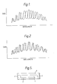
- FIG. 1 a schematic gain versus wavelength plot is shown for a laser amplifier in which the full line represents light propagating at one polarisation and the dotted line represents light propagating in the orthogonal polarisation.
- the illustrated plot shows the usual effect of the mode peaks for the orthogonal polarisations being misaligned due to their occurrence at slightly different wavelengths and with slightly different spacing. Due to a relatively small difference in the mode frequencies for the orthogonal polarisations the number of instances of mode peak matching (or beat frequency) is small, and so the probability of matching occurring at the gain peak is very small. It is for this reason that at particular operating wavelengths the gain sensitivity is generally found to be greater than that expected from the gain characteristic usually considered, which is the gain envelope.
- Figure 2 shows a similar schematic plot to that of Figure 1, however in this instance the plot is drawn for a device in accordance with the present invention that is fabricated with a difference in effective refractive index for the orthogonal polarisations such that there is a greater difference in the mode frequency.
- matching of the mode peaks occurs more frequently and thus the probability of matching occurring within the gain peak is much increased.
- the TE and TM gain envelopes are shown at substantially equal levels: this degree of equalisation would in fact be difficult to achieve, the Figures are drawn to demonstrate the mode coincidence aspect).
- the present invention proposes fabrication of a device with differences in the effective refractive index such that at least four mode peaks of the TE ripples are in phase with mode peaks of the TM ripples. This will provide a greater probability of mode peak alignment at the gain peaks, and/or also a greater number of wavelengths at which the gains are matched.
- the confinement factors should be made as close as possible so that the ripple envelopes are as close as possible.
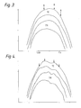
- Table 1 Device Average R.I. Difference in R.I. TM/TE Confinement Factor Ratio Gain Envelope Difference Actual peak difference A 3.5 0.03 0.91 2.5dB 5dB B 3.5 0.08 0.91 2.5dB 2.5dB C 3.5 0.08 0.85 3.0dB 3.0dB D 3.5 0.03 0.76 4.5dB 6.0dB E 3.5 0.08 0.76 4.5dB 4.5dB
- the refractive index difference can differ for a similar confinement factor.
- Devices B, C and E were exceptional in that they had unusually large differences in refractive index for TE and TM.
- the mode envelopes for two of the devices, D and E are shown in Figures 3 and 4. The gain differences in these instances between the mode envelopes are greater due to the lower confinement factor ratio, but nevertheless they demonstrate the frequency with which actual gain difference at peak gain approximates to the mode envelope gain difference.
- Figure 4 shows similar plots for one of the devices that was selected because of its unusually high difference in refractive index, in this case 0.08, in an average of 3.5.
- two in phase mode peaks were located in the 3dB bandwidth at wavelengths of approximately 1.49 microns and 1.51 microns, thus demonstrating an increase in frequency of occurrence over the laser amplifier of Figure 3, but for practical purposes (and even if the gain envelope gain difference were lower) this is an insufficient number of wavelengths at which matching occurs for practical purposes.
- devices are fabricated so that there are at least four wavelengths within the 3dB mode envelope bandwidth at which TE and TM mode peaks are in phase. For a 500 micron cavity length this can be achieved with an effective refractive index difference of 0.16: for a 1000 micron device it could be reduced to a difference of 0.08.
- n n* L 0.16 x 3.5 x 5 x 10 ⁇ 4 metres ⁇ 2.5 x 10 ⁇ 4
- L the cavity length of the laser
- Typical values of n* are 3.49 for TM and 3.61 for TE.
- the ratio of the TM/TE confinement factors is at least 0.9, and the mode frequency such that peak coincidence in phase modes occurs at least once every ten modes.
- n* gives rise to the different ripple frequencies.
- the aspect ratio required is preferably in excess of 10:1, more preferably in excess of 15:1 and most preferably in excess of 20:1. Having this degree of asymmetry in the waveguide makes the natural confinement across the short dimension much less than across the wider dimension. In order to equalise the confinement factors, as far as possible, the waveguide is bounded by layers which will increase the relative confinement across the short dimension.
- the boundary layers, or confinement layers may be made by stepping or grading the refractive index of the material around the waveguide, for example by different doping of the material or by different material composition, with the step in refractive index at the top and bottom of the waveguide being different (larger) than the step at the sides, the ratio of the material refractive index changes being in general correspondent with the aspect ratio.
- birefringent material either in the boundary layers or in the waveguide itself.
- birefringent material may be utilised to provide or assist in providing the necessary degree of refractive index difference without requiring, or enabling a reduction in the required, waveguide asymmetry.
- FIG. 5 illustrates a cross section through the active (or waveguiding) confinement layers of a laser amplifier.
- the device has an active layer 1 that is highly asymmetric having a width of the order of 3 microns and a depth of .15 microns. This strong asymmetry results in different propagation constants and thus in different effective refractive index for the TE and TM modes.
- the confinement factors need to be equalised as closely as possible, and this is achieved by having a different material refractive index step between the layer 1 and laterally bounding regions 2 than between the layer 1 and layers 3 above and below the active region.
- the absolute value of the steps must be such as to enable maintenance of single mode propagation within the waveguide. For example the required steps may be +.02 (in 3.5) above and below the waveguide and of the order of +.001 laterally of the waveguide.
- the materials from which the device may be fabricated are any of those from which a junction diode can be fabricated, including gallium arsenide, gallium phosphide, indium arsenide, indium phosphide and tertiary and quaternary materials formed from these.
- the present invention therefore proposes overcoming the polarisation sensitivity problem in laser amplifiers by increasing the difference in effective refractive index for TE and TM propagation modes to the level at which the beat frequency overlap of the mode ripples provides overlap within the 3dB mode envelope peak.
- the confinement factors are also made equal, or as close as possible, at the wavelengths corresponding to the mode ripple peak overlap the device is substantially polarisation insensitive.
- a practical way of bringing about the difference in effective refractive index is to have a highly asymmetric waveguide and to provide asymmetric lateral and vertical confinement steps or grading in the material of the refractive index. The problems that arise as a result of such a structure are that the spot is asymmetric and the device is wavelength sensitive.
- Suitable birefringent material may also remove this problem by replacing waveguide asymmetry, for example using a quantum well or multiple quantum well structure).
- wavelength sensitivity again this is acceptable where operation at a single, or few, wavelengths is required and maximum and/or polarisation insensitive gain is at a premium, for example in cascaded amplification where the cumulative effects of polarisation sensitivity of gain are a severe problem.
- the wavelength sensitivity of the polarisation insensitivity may be utilised to advantage. For example in multiply cascaded (with more than three stages) amplification where the signal is polarised, noise will be randomly polarised and at random wavelengths. In a polarisation sensitive system only the noise with the polarisation the same as the signal will be effectively amplified and the noise on the polarisation with less gain is effectively lost after several amplification stages.
- the device is polarisation sensitive off the transmission wavelength and so the reduction in noise gain operates the same as in a polarisation system, but at the transmission wavelengths the device has the advantage of polarisation insensitivity, and thus the device will provide a degree of filtering.
Landscapes
- Physics & Mathematics (AREA)
- Condensed Matter Physics & Semiconductors (AREA)
- General Physics & Mathematics (AREA)
- Electromagnetism (AREA)
- Optics & Photonics (AREA)
- Semiconductor Lasers (AREA)
- Lasers (AREA)
- Led Devices (AREA)
- Optical Integrated Circuits (AREA)
Applications Claiming Priority (2)
| Application Number | Priority Date | Filing Date | Title |
|---|---|---|---|
| GB8805016 | 1988-03-02 | ||
| GB888805016A GB8805016D0 (en) | 1988-03-02 | 1988-03-02 | Laser amplifier |
Publications (3)
| Publication Number | Publication Date |
|---|---|
| EP0331480A2 true EP0331480A2 (de) | 1989-09-06 |
| EP0331480A3 EP0331480A3 (en) | 1989-11-15 |
| EP0331480B1 EP0331480B1 (de) | 1994-05-25 |
Family
ID=10632743
Family Applications (1)
| Application Number | Title | Priority Date | Filing Date |
|---|---|---|---|
| EP89302067A Expired - Lifetime EP0331480B1 (de) | 1988-03-02 | 1989-03-01 | Laserverstärker |
Country Status (10)
| Country | Link |
|---|---|
| US (1) | US5132978A (de) |
| EP (1) | EP0331480B1 (de) |
| JP (1) | JPH03503090A (de) |
| AT (1) | ATE106170T1 (de) |
| AU (1) | AU629544B2 (de) |
| CA (1) | CA1322039C (de) |
| DE (1) | DE68915469T2 (de) |
| ES (1) | ES2052902T3 (de) |
| GB (1) | GB8805016D0 (de) |
| WO (1) | WO1989008340A2 (de) |
Families Citing this family (4)
| Publication number | Priority date | Publication date | Assignee | Title |
|---|---|---|---|---|
| JP3100641B2 (ja) * | 1990-12-18 | 2000-10-16 | 富士通株式会社 | 進行波型半導体光増幅装置 |
| US5425046A (en) * | 1992-06-11 | 1995-06-13 | Corning Incorporated | Optical collimating/polarizing device, method of making same and frequency stabilized laser using same |
| US6487232B1 (en) * | 1998-11-24 | 2002-11-26 | Agilent Technologies, Inc. | System and method for suppressing multimoding behavior of lasers |
| JP6927153B2 (ja) * | 2018-05-30 | 2021-08-25 | 日本電信電話株式会社 | 半導体レーザ |
Family Cites Families (8)
| Publication number | Priority date | Publication date | Assignee | Title |
|---|---|---|---|---|
| DE2248369A1 (de) * | 1972-10-03 | 1974-04-11 | Siemens Ag | Optischer zwischenverstaerker fuer ein nachrichtenuebertragungssystem |
| US4400052A (en) * | 1981-03-19 | 1983-08-23 | Bell Telephone Laboratories, Incorporated | Method for manufacturing birefringent integrated optics devices |
| CA1251846A (en) * | 1983-09-26 | 1989-03-28 | Masataka Shirasaki | Laser light source device |
| JPS60198879A (ja) * | 1984-03-23 | 1985-10-08 | Fujitsu Ltd | レ−ザ装置 |
| US4689797A (en) * | 1985-08-19 | 1987-08-25 | Gte Laboratories Incorporated | High power single spatial mode semiconductor laser |
| EP0354927A4 (en) * | 1987-08-19 | 1990-09-26 | Integrated Solar Technologies Corporation | Macro-gradient optical density transmissive light concentrators, lenses and compound lenses of large geometry, and fabrication thereof |
| GB8805620D0 (en) * | 1988-03-09 | 1988-04-07 | British Telecomm | Polarisation switching in active devices |
| US4918701A (en) * | 1988-09-27 | 1990-04-17 | Siemens Aktiengesellschaft | Semiconductor laser arrangement and method for the operation thereof |
-
1988
- 1988-03-02 GB GB888805016A patent/GB8805016D0/en active Pending
-
1989
- 1989-03-01 JP JP1503469A patent/JPH03503090A/ja active Pending
- 1989-03-01 AT AT89302067T patent/ATE106170T1/de not_active IP Right Cessation
- 1989-03-01 EP EP89302067A patent/EP0331480B1/de not_active Expired - Lifetime
- 1989-03-01 ES ES89302067T patent/ES2052902T3/es not_active Expired - Lifetime
- 1989-03-01 WO PCT/GB1989/000212 patent/WO1989008340A2/en not_active Ceased
- 1989-03-01 US US07/555,447 patent/US5132978A/en not_active Expired - Fee Related
- 1989-03-01 CA CA000592488A patent/CA1322039C/en not_active Expired - Fee Related
- 1989-03-01 AU AU32906/89A patent/AU629544B2/en not_active Ceased
- 1989-03-01 DE DE68915469T patent/DE68915469T2/de not_active Expired - Fee Related
Also Published As
| Publication number | Publication date |
|---|---|
| AU629544B2 (en) | 1992-10-08 |
| CA1322039C (en) | 1993-09-07 |
| WO1989008340A2 (en) | 1989-09-08 |
| US5132978A (en) | 1992-07-21 |
| WO1989008340A3 (en) | 1989-10-19 |
| ATE106170T1 (de) | 1994-06-15 |
| JPH03503090A (ja) | 1991-07-11 |
| EP0331480A3 (en) | 1989-11-15 |
| EP0331480B1 (de) | 1994-05-25 |
| AU3290689A (en) | 1989-09-22 |
| GB8805016D0 (en) | 1988-03-30 |
| DE68915469D1 (de) | 1994-06-30 |
| DE68915469T2 (de) | 1994-09-08 |
| ES2052902T3 (es) | 1994-07-16 |
Similar Documents
| Publication | Publication Date | Title |
|---|---|---|
| US4794346A (en) | Broadband semiconductor optical amplifier structure | |
| US6597497B2 (en) | Semiconductor optical amplifier with transverse laser cavity intersecting optical signal path and method of fabrication thereof | |
| US5930423A (en) | Semiconductor optical waveguide devices with integrated beam expander coupled to flat fibers | |
| US4750801A (en) | Optical waveguide resonator filters | |
| DE69534989T2 (de) | Integriertes optisches Regelelement und Verfahren zu seiner Herstellung und integriertoptisches Element und es verwendende integriertoptische Schaltkreisanordnung | |
| DE69307013T2 (de) | Integriertes, nichtlineares Wellenleiterspektrometer | |
| EP0546743A1 (de) | Phasenverschobener Halbleiterlaser mit verteilter Rückkoppelung | |
| EP0365724A1 (de) | Integrierte optische Wellenleiterkrümmung | |
| EP0262439B1 (de) | Lasersender mit einem Halbleiterlaser und einem externen Resonator | |
| JP3178565B2 (ja) | 半導体光デバイス | |
| US4952017A (en) | Polarization independent semiconductor optical amplifier | |
| DE69110605T2 (de) | Halbleiterlaser mit verteilter Rückkoppelung. | |
| DE69315949T2 (de) | Optischer Halbleiterverstärker | |
| US5522005A (en) | High power waveguide absorption modulator | |
| EP0578802A1 (de) | Vorrichtung und verfahren zur polarisationsunabhängigen signalverarbeitung mit kombiniertem wellenleiter und polarisationskonverter | |
| US6718094B1 (en) | Large surface amplifier with multimode interferometer | |
| EP0331480B1 (de) | Laserverstärker | |
| JP2001133647A (ja) | 導波路型高次モードフィルタおよび半導体レーザ | |
| Wada et al. | High-coupling-efficiency laser diodes integrated with spot-size converters fabricated on 2 inch InP substrates | |
| US4817106A (en) | Coupled waveguide injection laser | |
| US6259718B1 (en) | Distributed feedback laser device high in coupling efficiency with optical fiber | |
| DE69006518T2 (de) | Halbleiterlaser-Verstärker. | |
| US6608850B1 (en) | Semiconductor laser apparatus | |
| DE69210130T2 (de) | Optischer Verstärker mit einem Halbleiterlaser als Multiplexer | |
| DE60034768T2 (de) | Antireflektionsbeschichtung im signalband für eine pumpfacette |
Legal Events
| Date | Code | Title | Description |
|---|---|---|---|
| PUAI | Public reference made under article 153(3) epc to a published international application that has entered the european phase |
Free format text: ORIGINAL CODE: 0009012 |
|
| AK | Designated contracting states |
Kind code of ref document: A2 Designated state(s): AT BE CH DE ES FR GB GR IT LI LU NL SE |
|
| PUAL | Search report despatched |
Free format text: ORIGINAL CODE: 0009013 |
|
| AK | Designated contracting states |
Kind code of ref document: A3 Designated state(s): AT BE CH DE ES FR GB GR IT LI LU NL SE |
|
| 17P | Request for examination filed |
Effective date: 19900224 |
|
| 17Q | First examination report despatched |
Effective date: 19920818 |
|
| GRAA | (expected) grant |
Free format text: ORIGINAL CODE: 0009210 |
|
| AK | Designated contracting states |
Kind code of ref document: B1 Designated state(s): AT BE CH DE ES FR GB GR IT LI LU NL SE |
|
| PG25 | Lapsed in a contracting state [announced via postgrant information from national office to epo] |
Ref country code: GR Free format text: LAPSE BECAUSE OF FAILURE TO SUBMIT A TRANSLATION OF THE DESCRIPTION OR TO PAY THE FEE WITHIN THE PRESCRIBED TIME-LIMIT Effective date: 19940525 Ref country code: BE Effective date: 19940525 Ref country code: AT Effective date: 19940525 |
|
| REF | Corresponds to: |
Ref document number: 106170 Country of ref document: AT Date of ref document: 19940615 Kind code of ref document: T |
|
| ITF | It: translation for a ep patent filed | ||
| REF | Corresponds to: |
Ref document number: 68915469 Country of ref document: DE Date of ref document: 19940630 |
|
| REG | Reference to a national code |
Ref country code: ES Ref legal event code: FG2A Ref document number: 2052902 Country of ref document: ES Kind code of ref document: T3 |
|
| ET | Fr: translation filed | ||
| EAL | Se: european patent in force in sweden |
Ref document number: 89302067.7 |
|
| PLBE | No opposition filed within time limit |
Free format text: ORIGINAL CODE: 0009261 |
|
| STAA | Information on the status of an ep patent application or granted ep patent |
Free format text: STATUS: NO OPPOSITION FILED WITHIN TIME LIMIT |
|
| PG25 | Lapsed in a contracting state [announced via postgrant information from national office to epo] |
Ref country code: LU Free format text: LAPSE BECAUSE OF NON-PAYMENT OF DUE FEES Effective date: 19950331 |
|
| 26N | No opposition filed | ||
| PGFP | Annual fee paid to national office [announced via postgrant information from national office to epo] |
Ref country code: FR Payment date: 19960208 Year of fee payment: 8 |
|
| PGFP | Annual fee paid to national office [announced via postgrant information from national office to epo] |
Ref country code: SE Payment date: 19960214 Year of fee payment: 8 |
|
| PGFP | Annual fee paid to national office [announced via postgrant information from national office to epo] |
Ref country code: NL Payment date: 19960223 Year of fee payment: 8 |
|
| PGFP | Annual fee paid to national office [announced via postgrant information from national office to epo] |
Ref country code: DE Payment date: 19960227 Year of fee payment: 8 |
|
| PGFP | Annual fee paid to national office [announced via postgrant information from national office to epo] |
Ref country code: CH Payment date: 19960305 Year of fee payment: 8 |
|
| PGFP | Annual fee paid to national office [announced via postgrant information from national office to epo] |
Ref country code: ES Payment date: 19960308 Year of fee payment: 8 |
|
| PGFP | Annual fee paid to national office [announced via postgrant information from national office to epo] |
Ref country code: GB Payment date: 19970220 Year of fee payment: 9 |
|
| PG25 | Lapsed in a contracting state [announced via postgrant information from national office to epo] |
Ref country code: SE Effective date: 19970302 |
|
| PG25 | Lapsed in a contracting state [announced via postgrant information from national office to epo] |
Ref country code: ES Free format text: LAPSE BECAUSE OF NON-PAYMENT OF DUE FEES Effective date: 19970303 |
|
| PG25 | Lapsed in a contracting state [announced via postgrant information from national office to epo] |
Ref country code: LI Effective date: 19970331 Ref country code: CH Effective date: 19970331 |
|
| PG25 | Lapsed in a contracting state [announced via postgrant information from national office to epo] |
Ref country code: NL Effective date: 19971001 |
|
| REG | Reference to a national code |
Ref country code: CH Ref legal event code: PL |
|
| PG25 | Lapsed in a contracting state [announced via postgrant information from national office to epo] |
Ref country code: FR Free format text: LAPSE BECAUSE OF NON-PAYMENT OF DUE FEES Effective date: 19971128 |
|
| NLV4 | Nl: lapsed or anulled due to non-payment of the annual fee |
Effective date: 19971001 |
|
| PG25 | Lapsed in a contracting state [announced via postgrant information from national office to epo] |
Ref country code: DE Effective date: 19971202 |
|
| EUG | Se: european patent has lapsed |
Ref document number: 89302067.7 |
|
| REG | Reference to a national code |
Ref country code: FR Ref legal event code: ST |
|
| PG25 | Lapsed in a contracting state [announced via postgrant information from national office to epo] |
Ref country code: GB Free format text: LAPSE BECAUSE OF NON-PAYMENT OF DUE FEES Effective date: 19980301 |
|
| GBPC | Gb: european patent ceased through non-payment of renewal fee |
Effective date: 19980301 |
|
| REG | Reference to a national code |
Ref country code: ES Ref legal event code: FD2A Effective date: 19990301 |
|
| PG25 | Lapsed in a contracting state [announced via postgrant information from national office to epo] |
Ref country code: IT Free format text: LAPSE BECAUSE OF NON-PAYMENT OF DUE FEES Effective date: 20050301 |