EP0331437A2 - Charakterisierung von Fotolackmaterialien für Halbleiter während der Verarbeitung - Google Patents
Charakterisierung von Fotolackmaterialien für Halbleiter während der Verarbeitung Download PDFInfo
- Publication number
- EP0331437A2 EP0331437A2 EP89301987A EP89301987A EP0331437A2 EP 0331437 A2 EP0331437 A2 EP 0331437A2 EP 89301987 A EP89301987 A EP 89301987A EP 89301987 A EP89301987 A EP 89301987A EP 0331437 A2 EP0331437 A2 EP 0331437A2
- Authority
- EP
- European Patent Office
- Prior art keywords
- resist film
- predetermined
- substrate
- film
- resist
- Prior art date
- Legal status (The legal status is an assumption and is not a legal conclusion. Google has not performed a legal analysis and makes no representation as to the accuracy of the status listed.)
- Withdrawn
Links
- 239000000463 material Substances 0.000 title claims abstract description 63
- 239000004065 semiconductor Substances 0.000 title claims abstract description 6
- 238000012545 processing Methods 0.000 title description 2
- 238000012512 characterization method Methods 0.000 title 1
- 238000000034 method Methods 0.000 claims abstract description 84
- 238000010521 absorption reaction Methods 0.000 claims abstract description 30
- 230000008569 process Effects 0.000 claims abstract description 25
- 239000000758 substrate Substances 0.000 claims description 43
- 238000002310 reflectometry Methods 0.000 claims description 35
- 239000002904 solvent Substances 0.000 claims description 26
- 238000005259 measurement Methods 0.000 claims description 17
- 230000003287 optical effect Effects 0.000 claims description 10
- 238000000151 deposition Methods 0.000 claims 2
- 238000012544 monitoring process Methods 0.000 abstract description 2
- 229920002120 photoresistant polymer Polymers 0.000 description 18
- 235000012431 wafers Nutrition 0.000 description 9
- 230000005540 biological transmission Effects 0.000 description 6
- 238000000576 coating method Methods 0.000 description 6
- 230000000875 corresponding effect Effects 0.000 description 6
- 230000008859 change Effects 0.000 description 4
- 239000000470 constituent Substances 0.000 description 4
- 239000011248 coating agent Substances 0.000 description 3
- 230000007423 decrease Effects 0.000 description 3
- 238000004090 dissolution Methods 0.000 description 3
- 230000014509 gene expression Effects 0.000 description 3
- 239000007788 liquid Substances 0.000 description 3
- 230000005855 radiation Effects 0.000 description 3
- 238000004132 cross linking Methods 0.000 description 2
- 230000000694 effects Effects 0.000 description 2
- 230000005670 electromagnetic radiation Effects 0.000 description 2
- 238000005530 etching Methods 0.000 description 2
- 238000011156 evaluation Methods 0.000 description 2
- 238000001704 evaporation Methods 0.000 description 2
- 230000008020 evaporation Effects 0.000 description 2
- 150000002500 ions Chemical class 0.000 description 2
- 238000004519 manufacturing process Methods 0.000 description 2
- 239000002245 particle Substances 0.000 description 2
- 230000010287 polarization Effects 0.000 description 2
- 229920000642 polymer Polymers 0.000 description 2
- 238000006116 polymerization reaction Methods 0.000 description 2
- 230000035945 sensitivity Effects 0.000 description 2
- LIPRQQHINVWJCH-UHFFFAOYSA-N 1-ethoxypropan-2-yl acetate Chemical compound CCOCC(C)OC(C)=O LIPRQQHINVWJCH-UHFFFAOYSA-N 0.000 description 1
- SVONRAPFKPVNKG-UHFFFAOYSA-N 2-ethoxyethyl acetate Chemical compound CCOCCOC(C)=O SVONRAPFKPVNKG-UHFFFAOYSA-N 0.000 description 1
- 229910001218 Gallium arsenide Inorganic materials 0.000 description 1
- CTQNGGLPUBDAKN-UHFFFAOYSA-N O-Xylene Chemical compound CC1=CC=CC=C1C CTQNGGLPUBDAKN-UHFFFAOYSA-N 0.000 description 1
- 206010034972 Photosensitivity reaction Diseases 0.000 description 1
- 230000009471 action Effects 0.000 description 1
- 238000013459 approach Methods 0.000 description 1
- 238000003491 array Methods 0.000 description 1
- 238000006243 chemical reaction Methods 0.000 description 1
- 230000002596 correlated effect Effects 0.000 description 1
- 238000000354 decomposition reaction Methods 0.000 description 1
- 230000001066 destructive effect Effects 0.000 description 1
- 238000009826 distribution Methods 0.000 description 1
- 230000005684 electric field Effects 0.000 description 1
- 238000010894 electron beam technology Methods 0.000 description 1
- 238000000572 ellipsometry Methods 0.000 description 1
- 238000005516 engineering process Methods 0.000 description 1
- 238000010884 ion-beam technique Methods 0.000 description 1
- 230000031700 light absorption Effects 0.000 description 1
- 230000004048 modification Effects 0.000 description 1
- 238000012986 modification Methods 0.000 description 1
- 229920000620 organic polymer Polymers 0.000 description 1
- 238000001615 p wave Methods 0.000 description 1
- 230000036211 photosensitivity Effects 0.000 description 1
- 239000003504 photosensitizing agent Substances 0.000 description 1
- 238000002360 preparation method Methods 0.000 description 1
- 230000009467 reduction Effects 0.000 description 1
- 230000004044 response Effects 0.000 description 1
- 238000007761 roller coating Methods 0.000 description 1
- 239000007787 solid Substances 0.000 description 1
- 239000007921 spray Substances 0.000 description 1
- 238000005507 spraying Methods 0.000 description 1
- 239000000126 substance Substances 0.000 description 1
- 230000008961 swelling Effects 0.000 description 1
- 238000003079 width control Methods 0.000 description 1
- 239000008096 xylene Substances 0.000 description 1
Images


Classifications
-
- G—PHYSICS
- G03—PHOTOGRAPHY; CINEMATOGRAPHY; ANALOGOUS TECHNIQUES USING WAVES OTHER THAN OPTICAL WAVES; ELECTROGRAPHY; HOLOGRAPHY
- G03F—PHOTOMECHANICAL PRODUCTION OF TEXTURED OR PATTERNED SURFACES, e.g. FOR PRINTING, FOR PROCESSING OF SEMICONDUCTOR DEVICES; MATERIALS THEREFOR; ORIGINALS THEREFOR; APPARATUS SPECIALLY ADAPTED THEREFOR
- G03F7/00—Photomechanical, e.g. photolithographic, production of textured or patterned surfaces, e.g. printing surfaces; Materials therefor, e.g. comprising photoresists; Apparatus specially adapted therefor
- G03F7/16—Coating processes; Apparatus therefor
- G03F7/168—Finishing the coated layer, e.g. drying, baking, soaking
Definitions
- This invention relates to determination of semiconductor resist material parameters such as percentage of solvent remaining during resist fabrication processes such as softbake.
- Photoresist and other resist material such as electron beam or ion beam resist is used in semiconductor processing to fabricate masks that allow etching of selected portions of a chip at any level.
- Resist materials are usually organic polymers that change state in response to irradiation of small portions of the resist material by a beam of photons (visible, ultraviolet, X-ray) or charged particles such as electrons or ions.
- irradiation produces local decomposition of the resist constituents into lower molecular weight polymers so that the etchant attacks these areas more readily than it attacks constituents in the unirradiated areas.
- irradiation produces cross-linking among the polymers so that the resulting higher molecular weight constituents resist etching action more successfully than do constituents in the unirradiated areas.
- This cross-linking produces a swelling on negative resist material so that optical resolution in a negative resist is usually limited to 1.5 ⁇ m or more.
- positive and negative resist materials are initially fabricated in a similar manner.
- the substrate is often oxidized or unoxidized Si or GaAs, doped or undoped.
- One purpose of this invention is to provide a method for quantitatively monitoring certain changes induced in a film of resist material as the material is processed in the resist coating and/or softbake operations.
- the method in one embodiment may include the steps of: determining the thickness of the resist film through a measurement of Total Reflectivity of the resist film at each of a sequence of one or more predetermined wave lengths ⁇ 1, ⁇ 2, ..., ⁇ r at a sequence of one or more predetermined film incidence angles ⁇ 1.1 , ⁇ 1.2 , ..., 6i,s (with r + s > 3); and determining the absorption of the resist material after the coat process and before completion of the softbake process through a measurement of Total Reflectivity or Total Transmissivity of the resist film for a predetermined wavelength ⁇ , a predetermined film incidence angle 8 1 and predetermined film thickness.
- Photoresist and other resist material is normally applied and used in three or more phases.
- the resist liquid (or gel) is applied at an approximate thickness (usually 100 ⁇ m or more) to one planar surface of a substrate, and the substrate is spun about a central axis to throw off a portion of the resist by centrifugal force and reduce the resist film thickness to a first thickness, as yet unknown.
- the resist includes both the sensitizer (solute) and the more volatile solvent or liquid vehicle; the solvent continues to evaporate so that film thickness varies with time.
- the solvent is substantially transparent and any absorption in the resist material is due substantially wholly to the solute present in the resist material.
- the absorption will be independent of resist thickness; and a measurement of absorption will not vary as solvent (only) is removed from the resist material.
- This definition of absorption uses the well-known Beers-Lambert law for absorption of light, which is a reasonably accurate first approximation for such absorption.
- the solvent volatilises and leaves the resist solution, through softbake by infrared or microwave irradiation or evaporation at high ambient temperature for a relatively short time interval (10-60 seconds).
- the fraction of the resist liquid decreases during softbake from 30-60 weight percent before softbake to 10-20 weight percent at the completion of softbake. This is sometimes referred to as "curing" the resist.
- Negative resist materials have a similar problem; under-softbaking leads to incomplete polymerization in exposed areas of the resist, and the exposed and unexposed areas are attacked more easily, with a concomitant fall in contrast. Contrast is defined here as the ratio where I max and I min are the maximum and minimum radiation intensities, respectively, sensed through the exposed and developed (etched) resist.
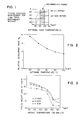
- This characteristic, higher dissolution rate of the resist material as one decreases T soft is illustrated generically in Figure 2.
- dissolution rate R d is determined by T soft , by the time interval ⁇ t soft of softbake, and by the manner (convection, conduction, infrared, microwave, rf, etc.) in which the thermal energy is delivered.
- R d depends upon all these variables and also upon degree of polymerization of the resist material.
- the solvent percentage varies over a narrow range, over which the refractive index of the solute/solvent combination is substantially constant and thus can be determined ab initio.
- the refractive index of a resist material appears to decrease monotonically with increasing dose (mJ/cm 2 ), as illustrated in Figure 5 for five resist materials, Shipley AZ-1350B, 1350J, 1370, 4110 and 5214.
- a central idea here is to use changes in particular chemical and physical characteristics of the resist material as it is processed to independently monitor or evaluate the quality of the coating process and the softbake process.
- the invention is applicable to positive resist and photoresist materials, including Kodak Micro Resist 809, Hunt Waycoat HPR 204 and 206, Ohka OFPR-800, MIT IC 528, and Shipley AZ 111S, 111H, 1350J, 1370, 1450J and 2400.
- the invention is also applicable to negative resist and photoresist materials, including Kodak Micro Resist 747 and 752, Hunt Waycoat HNR 80, HNR 120, SC 100 and HR 100, MIT Isopoly MR and HD, Ohka OSR, and KTI 732, 747 and 752.
- Positive and negative resists use different solvents as well as different photosensitizers.
- the AZ 1350 and 1370 positive photoresists use 2-ethoxylethyl acetate, and AZ 1512 and 1518 use propylene glycol monoethyl ether acetate as solvent; and the KTI negative photoresists 732, 747 and 752 use xylene as solvent.
- Typical recommended doses of positive resist materials e.g., 80-256 millijoules/cm 2 for Kodak Micro Resist 809 appear to be two to five times as large as typical recommended doses for negative resist materials of similar thicknesses and wavelengths (e.g., 45-55 millijoules/cm 2 for Kodak 747).
- the Tan et al. application discloses a first method (herein called the "Reflectivity Inversion Method") for determining thickness h of the film (having predetermined refractive index n2( ⁇ 1)) by appropriately inverting the equation
- a second method for thickness determination disclosed in the Tan et al. application begins with a fixed incidence angle ⁇ 1 , a sequence of predetermined film thickness numbers with h min ⁇ hi ⁇ h 2 ⁇ ...
- the Total Reflectivity values R are computed for each of a sequence of predetermined incidence angles (v > 2) and a fixed wavelength ⁇ 1; this yields an array of Total Reflectivity values R ( ⁇ 1,g ; ⁇ 1 ; hi), where hi as before is drawn from a sequence of predetermined thickness numbers . Reflectivity measurements are made on the film/substrate combination with unknown film thickness at each incidence angle ⁇ 1,g at the wavelength ⁇ 1 ; these yield a sequence of measurements .
- the absorption a o 1 - e -( ⁇ L)0 of the bare substrate surface is first measured and stored.
- the single parameter (aL)o measures any absorption or related anomalies that occur at the surface of the bare substrate, based upon substrate refractive index and theoretical reflectivity of the substrate surface.
- the resist material is then deposited on one or a plurality of wafers (20 is a convenient batch size) at estimated thicknesses of 1 ⁇ m, and the wafers are spun.
- the wafers are then allowed to settle for a period of time (optional), and coating thickness is measured for each wafer, using measurement of Total Reflectivity such as the Reflectivity Inversion Method, the Reflectivity Versus Wavelength Variance Method or the Reflectivity Versus Incidence Angle Variance Method discussed above, or any other suitable method such as ellipsometry.
- the wavelength(s) ⁇ or irradiation for the thickness determination should be chosen so that the refractive index n( ⁇ ) is real, or substantially so.
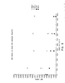
- Figures 6, 7 and 8 illustrate the percentage transmission of three representative Hoechst positive resist materials, AZ 1370, AZ 4110 and AZ 5214-E as a function of irradiation wavelength ⁇ for thicknesses of 1 ⁇ m, 1 ⁇ m and 1.15 ⁇ m, respectively.
- E the electric field strength vector
- This method may be drawn from the Simple Reflectivity Method, the Complex Reflectivity Method, the Simple Transmissivity Method, the Complex Transmissivity Method, or any other suitable method that works with all orders of optical interferences, to determine a or a.
- the resist solvent is substantially transparent at the wavelengths of interest allows one to decouple an evaluation of the coat process, using determinations of thickness h and absorptivity coefficient a after coating and before softbake, from an evaluation of the softbake process, using post-softbake values for h.
- A should be the same for each wafer, indicating that the solute molecules are uniformly distributed throughout the batch of wafers being tested.
- the parameter A represents "true" absorptivity of the resist material itself; A for each wafer should lie within a narrow range, say ⁇ one percent of the target value At for that resist material.
- At may be taken as the arithmetic mean of all the values of A in this batch.
- p h(after softbake)/A This provides a measure of absorption in the resist film due to the solute molecules, which are assumed to be substantially the only molecules that contribute to absorption.
- pt h(after softbake)/A
- the most important feature here is the fact that the coat and softbake processes can now be monitored separately and independently for compliance with predetermined standards for each of these processes.
- This approach resolves two problems perceived by many workers in this field: (1) After coat and before softbake stabilizes the resist film, the thickness h continues to vary with time as evaporation proceeds; one solution is to use the absorptivity coefficient a, which is assumed to arise from the presence of only the solute molecules in the resist of the irradiation wavelength chosen; (2) During the softbake process, one has two parameters (A and h) to work with, with differing units; one solution here is to form the product or the ratio of these two monitor parameters.
Landscapes
- Physics & Mathematics (AREA)
- General Physics & Mathematics (AREA)
- Length Measuring Devices By Optical Means (AREA)
- Testing Or Measuring Of Semiconductors Or The Like (AREA)
- Photosensitive Polymer And Photoresist Processing (AREA)
Applications Claiming Priority (2)
| Application Number | Priority Date | Filing Date | Title |
|---|---|---|---|
| US07/162,431 US4874240A (en) | 1988-03-01 | 1988-03-01 | Characterization of semiconductor resist material during processing |
| US162431 | 2002-06-04 |
Publications (2)
| Publication Number | Publication Date |
|---|---|
| EP0331437A2 true EP0331437A2 (de) | 1989-09-06 |
| EP0331437A3 EP0331437A3 (de) | 1991-08-21 |
Family
ID=22585593
Family Applications (1)
| Application Number | Title | Priority Date | Filing Date |
|---|---|---|---|
| EP19890301987 Withdrawn EP0331437A3 (de) | 1988-03-01 | 1989-02-28 | Charakterisierung von Fotolackmaterialien für Halbleiter während der Verarbeitung |
Country Status (3)
| Country | Link |
|---|---|
| US (1) | US4874240A (de) |
| EP (1) | EP0331437A3 (de) |
| JP (1) | JPH027052A (de) |
Cited By (1)
| Publication number | Priority date | Publication date | Assignee | Title |
|---|---|---|---|---|
| WO2003005003A1 (de) * | 2001-06-29 | 2003-01-16 | Zentrum Mikroelektronik Dresden Ag | Verfahren zur bestimmung des schichtwiderstandes einer oberflächenschicht |
Families Citing this family (5)
| Publication number | Priority date | Publication date | Assignee | Title |
|---|---|---|---|---|
| US5293216A (en) * | 1990-12-31 | 1994-03-08 | Texas Instruments Incorporated | Sensor for semiconductor device manufacturing process control |
| US5216487A (en) * | 1991-05-22 | 1993-06-01 | Site Services, Inc. | Transmissive system for characterizing materials containing photoreactive constituents |
| WO1994002832A1 (en) * | 1992-07-15 | 1994-02-03 | On-Line Technologies, Inc. | Method and apparatus for monitoring layer processing |
| US5494697A (en) * | 1993-11-15 | 1996-02-27 | At&T Corp. | Process for fabricating a device using an ellipsometric technique |
| US6455073B1 (en) | 2000-07-10 | 2002-09-24 | Enzrel, Inc. | Covalent microparticle-drug conjugates for biological targeting |
Family Cites Families (1)
| Publication number | Priority date | Publication date | Assignee | Title |
|---|---|---|---|---|
| DE3406645A1 (de) * | 1984-02-24 | 1985-08-29 | Leybold-Heraeus GmbH, 5000 Köln | Spektralfotometeranordnung |
-
1988
- 1988-03-01 US US07/162,431 patent/US4874240A/en not_active Expired - Fee Related
-
1989
- 1989-02-28 JP JP1048401A patent/JPH027052A/ja active Pending
- 1989-02-28 EP EP19890301987 patent/EP0331437A3/de not_active Withdrawn
Non-Patent Citations (1)
| Title |
|---|
| CHEMICAL ABSTRACTS, vol. 99, no. 6, August 1983 Columbus, Ohio, USA Takami K. et al: "Thickness measurement method for thin photoresist film on transparentmaterial" ref. no. 4598E * |
Cited By (1)
| Publication number | Priority date | Publication date | Assignee | Title |
|---|---|---|---|---|
| WO2003005003A1 (de) * | 2001-06-29 | 2003-01-16 | Zentrum Mikroelektronik Dresden Ag | Verfahren zur bestimmung des schichtwiderstandes einer oberflächenschicht |
Also Published As
| Publication number | Publication date |
|---|---|
| EP0331437A3 (de) | 1991-08-21 |
| US4874240A (en) | 1989-10-17 |
| JPH027052A (ja) | 1990-01-11 |
Similar Documents
| Publication | Publication Date | Title |
|---|---|---|
| US5124216A (en) | Method for monitoring photoresist latent images | |
| US5597868A (en) | Polymeric anti-reflective compounds | |
| US6403152B1 (en) | Anti-reflective coating compositions comprising polymerized aminoplasts | |
| US20040257588A1 (en) | Parametric profiling using optical spectroscopic systems | |
| EP0436639B1 (de) | Multifunktionelle photolithographische zusammensetzungen | |
| US4414314A (en) | Resolution in optical lithography | |
| US4874240A (en) | Characterization of semiconductor resist material during processing | |
| US5110697A (en) | Multifunctional photolithographic compositions | |
| CN101424877A (zh) | 包含酚醛清漆树脂共混物的光刻胶 | |
| WO1997033201A1 (en) | Bottom antireflective coatings through refractive index modification by anomalous dispersion | |
| US6252670B1 (en) | Method for accurately calibrating a constant-angle reflection-interference spectrometer (CARIS) for measuring photoresist thickness | |
| US5982496A (en) | Thin film thickness and optimal focus measuring using reflectivity | |
| US5066561A (en) | Method for producing and using a positive photoresist with o-quinone diazide, novolak, and propylene glycol alkyl ether acetate | |
| JPS6024548A (ja) | ホトレジスト被覆表面の露出条件の選択方法 | |
| Boher et al. | Characterization of resists and antireflective coatings by spectroscopic ellipsometry in the UV and deep-UV range | |
| Gamsky et al. | Infrared reflection absorption spectroscopy of photoresist films on silicon wafers: measuring film thickness and removing interference fringes | |
| Spence et al. | Silylation of poly (t-BOC) styrene resists: performance and mechanisms | |
| Kim et al. | In-situ non-contact monitoring of photoresist thickness and degree of cure using terahertz time-domain spectroscopy | |
| WO1998048263A1 (en) | Method for monitoring the parameters of film coatings and surfaces during their modification process and device for realising the same | |
| IL94353A (en) | Novolak-containing photoresist composition | |
| Sakaida et al. | Multilayer BARCs for hyper-NA immersion lithography process | |
| JPH1055072A (ja) | レジストパターン形成方法及びレジストパターン形成装置 | |
| Park et al. | Roughness of EUV resists exposed to EUV, ArF and KrF radiation as evaluated using three tools: spectroscopic ellipsometry, AFM and SEM | |
| Seiji Takeuchi et al. | New ellipsometric approach to critical dimension metrology utilizing form birefringence inherent in a submicron line-and-space pattern | |
| Sautter et al. | Development Process Control And Optimization Utilizing An End Point Monitor |
Legal Events
| Date | Code | Title | Description |
|---|---|---|---|
| PUAI | Public reference made under article 153(3) epc to a published international application that has entered the european phase |
Free format text: ORIGINAL CODE: 0009012 |
|
| AK | Designated contracting states |
Kind code of ref document: A2 Designated state(s): AT BE CH DE ES FR GB GR IT LI LU NL SE |
|
| PUAL | Search report despatched |
Free format text: ORIGINAL CODE: 0009013 |
|
| AK | Designated contracting states |
Kind code of ref document: A3 Designated state(s): AT BE CH DE ES FR GB GR IT LI LU NL SE |
|
| 17P | Request for examination filed |
Effective date: 19920127 |
|
| 17Q | First examination report despatched |
Effective date: 19921112 |
|
| STAA | Information on the status of an ep patent application or granted ep patent |
Free format text: STATUS: THE APPLICATION IS DEEMED TO BE WITHDRAWN |
|
| 18D | Application deemed to be withdrawn |
Effective date: 19940209 |