EP0330404A2 - Integrated circuit cards - Google Patents
Integrated circuit cards Download PDFInfo
- Publication number
- EP0330404A2 EP0330404A2 EP89301626A EP89301626A EP0330404A2 EP 0330404 A2 EP0330404 A2 EP 0330404A2 EP 89301626 A EP89301626 A EP 89301626A EP 89301626 A EP89301626 A EP 89301626A EP 0330404 A2 EP0330404 A2 EP 0330404A2
- Authority
- EP
- European Patent Office
- Prior art keywords
- card
- memory
- data
- read
- set forth
- Prior art date
- Legal status (The legal status is an assumption and is not a legal conclusion. Google has not performed a legal analysis and makes no representation as to the accuracy of the status listed.)
- Granted
Links
Images


Classifications
-
- G—PHYSICS
- G07—CHECKING-DEVICES
- G07F—COIN-FREED OR LIKE APPARATUS
- G07F7/00—Mechanisms actuated by objects other than coins to free or to actuate vending, hiring, coin or paper currency dispensing or refunding apparatus
- G07F7/08—Mechanisms actuated by objects other than coins to free or to actuate vending, hiring, coin or paper currency dispensing or refunding apparatus by coded identity card or credit card or other personal identification means
- G07F7/10—Mechanisms actuated by objects other than coins to free or to actuate vending, hiring, coin or paper currency dispensing or refunding apparatus by coded identity card or credit card or other personal identification means together with a coded signal, e.g. in the form of personal identification information, like personal identification number [PIN] or biometric data
- G07F7/1008—Active credit-cards provided with means to personalise their use, e.g. with PIN-introduction/comparison system
-
- G—PHYSICS
- G06—COMPUTING; CALCULATING OR COUNTING
- G06Q—INFORMATION AND COMMUNICATION TECHNOLOGY [ICT] SPECIALLY ADAPTED FOR ADMINISTRATIVE, COMMERCIAL, FINANCIAL, MANAGERIAL OR SUPERVISORY PURPOSES; SYSTEMS OR METHODS SPECIALLY ADAPTED FOR ADMINISTRATIVE, COMMERCIAL, FINANCIAL, MANAGERIAL OR SUPERVISORY PURPOSES, NOT OTHERWISE PROVIDED FOR
- G06Q20/00—Payment architectures, schemes or protocols
- G06Q20/30—Payment architectures, schemes or protocols characterised by the use of specific devices or networks
- G06Q20/34—Payment architectures, schemes or protocols characterised by the use of specific devices or networks using cards, e.g. integrated circuit [IC] cards or magnetic cards
- G06Q20/341—Active cards, i.e. cards including their own processing means, e.g. including an IC or chip
-
- G—PHYSICS
- G06—COMPUTING; CALCULATING OR COUNTING
- G06Q—INFORMATION AND COMMUNICATION TECHNOLOGY [ICT] SPECIALLY ADAPTED FOR ADMINISTRATIVE, COMMERCIAL, FINANCIAL, MANAGERIAL OR SUPERVISORY PURPOSES; SYSTEMS OR METHODS SPECIALLY ADAPTED FOR ADMINISTRATIVE, COMMERCIAL, FINANCIAL, MANAGERIAL OR SUPERVISORY PURPOSES, NOT OTHERWISE PROVIDED FOR
- G06Q20/00—Payment architectures, schemes or protocols
- G06Q20/30—Payment architectures, schemes or protocols characterised by the use of specific devices or networks
- G06Q20/34—Payment architectures, schemes or protocols characterised by the use of specific devices or networks using cards, e.g. integrated circuit [IC] cards or magnetic cards
- G06Q20/357—Cards having a plurality of specified features
- G06Q20/3576—Multiple memory zones on card
-
- G—PHYSICS
- G06—COMPUTING; CALCULATING OR COUNTING
- G06Q—INFORMATION AND COMMUNICATION TECHNOLOGY [ICT] SPECIALLY ADAPTED FOR ADMINISTRATIVE, COMMERCIAL, FINANCIAL, MANAGERIAL OR SUPERVISORY PURPOSES; SYSTEMS OR METHODS SPECIALLY ADAPTED FOR ADMINISTRATIVE, COMMERCIAL, FINANCIAL, MANAGERIAL OR SUPERVISORY PURPOSES, NOT OTHERWISE PROVIDED FOR
- G06Q20/00—Payment architectures, schemes or protocols
- G06Q20/30—Payment architectures, schemes or protocols characterised by the use of specific devices or networks
- G06Q20/36—Payment architectures, schemes or protocols characterised by the use of specific devices or networks using electronic wallets or electronic money safes
- G06Q20/367—Payment architectures, schemes or protocols characterised by the use of specific devices or networks using electronic wallets or electronic money safes involving electronic purses or money safes
-
- G—PHYSICS
- G06—COMPUTING; CALCULATING OR COUNTING
- G06Q—INFORMATION AND COMMUNICATION TECHNOLOGY [ICT] SPECIALLY ADAPTED FOR ADMINISTRATIVE, COMMERCIAL, FINANCIAL, MANAGERIAL OR SUPERVISORY PURPOSES; SYSTEMS OR METHODS SPECIALLY ADAPTED FOR ADMINISTRATIVE, COMMERCIAL, FINANCIAL, MANAGERIAL OR SUPERVISORY PURPOSES, NOT OTHERWISE PROVIDED FOR
- G06Q20/00—Payment architectures, schemes or protocols
- G06Q20/38—Payment protocols; Details thereof
- G06Q20/382—Payment protocols; Details thereof insuring higher security of transaction
- G06Q20/3829—Payment protocols; Details thereof insuring higher security of transaction involving key management
Definitions
- the present invention relates to integrated circuit cards (hereinafter referred to as IC cards).
- one form of prior art IC card contains a processor, i.e. a central processing unit (CPU) and a memory, both packaged in a plastic plate as one body.
- the capacity of the memory might typically be 8K bytes, but such memory capacity may not be sufficient when the facilities provided by the IC card are to be expanded.
- a laser memory card may be provided separately.
- a laser memory card has a memory which can be written and read by laser light. The capacity of the laser card can be several million bytes. In the known art, however, such a laser card is physically and logically separated from the IC card.
- the laser memory can be used only when a special external terminal machine, i.e. a special card acceptance means, is available, and this, of course, is inconvenient.
- An alternative form of IC card system has been considered, having a magnetic stripe thereon, in which information recorded on the magnetic stripe is read and handled by a processor separate from the internal processor of the IC card.
- the internal processor only reads and handles information stored in an internal memory of the card.
- the IC card is provided with an internal processor (CPU) which includes communication means for controlling an external auxiliary memory, provided integrally with the body of the IC card, by an external card acceptance means.
- CPU central processing unit
- An IC card system embodying the present invention desirably provides protection against illegal access to information in the external memory, and can advantageously provide an IC card system in which records relating to past access to information recorded in the external memory (update history) can be easily obtained by an authorised user after verification.
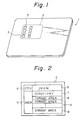
- FIG 1 is a perspective view of a conventional IC card.
- reference 1 represents an IC card.
- the IC card 1 contains an integrated circuit module 2 comprising a processor (CPU) and an internal memory (neither of which are shown).
- the CPU and the memory transmit and receive data to and from external card acceptance means via a plurality of contacts 3.
- Figure 1 shows the rear surface of the IC card; the front surface thereof has a variety of devices mounted thereon, such as a display unit, a ten key unit, and so on.
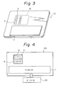
- FIG. 2 is a schematic diagram of an internal construction of an integrated circuit module.
- the main components of the integrated circuit module 2 are the processor (CPU) 4 and the internal memory (IMEM) 5.
- the CPU 4 forms an IC card access means 6 and the memory, generally a main memory, forms a plurality of format areas 8; these format areas 8 also define a file 9.
- the internal memory access means (IMAM) 6 sets up an operating system and is able to process an access of the IC card 1 to the external IC card acceptance means.
- a search is first made of the directory 7, which is a dictionary storing file numbers (Nos.).
- the memory comprises an IC memory, for example, an electronically erasable programmable read only memory (EEPROM).
- IC memory for example, an electronically erasable programmable read only memory (EEPROM).
- the capacity of the IC memory might typically be 8 K bytes.
- a laser memory card may be used an an accessory to the IC card.
- it is inconvenient to utilize a laser memory card with an IC card despite the very large memory capacity of the laser memory card.
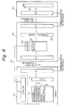
- an IC card of a system embodying the present invention is provided with an external memory 11 mounted on the surface of the body of the IC card 20 to form a monolithic structure.
- the external memory 11 is adhered to the body of the IC card 20. As such, the external memory 11 is physically and logically separated from the integrated circuit module 12.
- FIG. 4 is a schematic diagram of an arrangement of devices in an IC card of a system embodying the present invention.
- the IC card 20 contains the processor (CPU) 4 and the internal memory (IMEM) 5, i.e. a main memory, both formed as the integrated circuit module 12, i.e., an IC chip.
- the contacts (shown by 3 in Fig. 3 but not illustrated in Fig. 4) are used for data communication between the processor 4, together with the internal memory 5, and the external IC card acceptance means.
- the external memory (EMEM) 11 does not perform data communication via the contacts 3, but communicates directly with the external IC card acceptance means, as illustrated by a two-way arrow in Fig. 4. Accordingly, only the CPU 4 can manage the external memory 11.
- identical components are represented by the same reference numerals or characters throughout the drawings.
- FIG. 5 is a schematic diagram of the general construction of devices mounted on and in an IC card of a system embodying to the present invention.
- the processor (CPU) 4 is usually provided with a program ROM which creates therein the internal memory access means (IMAM) 6 and the external memory access means (EMAM) 23 of the present invention. Namely, the means (IMAM) 6 and the means (EMAM) 23 are actually established as programs.
- the internal memory (IMEM) 5 is preferably a non-volatile memory, such as an EEPROM, and has a first directory 21 and a second directory 22 formed therein.
- the second directory 22 defines the format areas 8 of the file 9 allotted for the internal memory per se (main memory), and thus the second directory 22 is substantially the same as the directory 7 shown in Fig. 2.
- the first directory 21, however, defines the format areas 8 of the file 9 allotted for the external memory 11.
- the format areas 8 and format areas 17 (explained below) store user data relating to the IC card owner.
- the external memory 11 is composed of a password area 17 and the format areas 18 setting up a file 19.
- the password in the area 17 is used in an authentication check of the external memory 11 performed by the internal processor.
- the external memory (EMEM) 11 can have a memory capacity much larger than that of the internal memory (IMEM) 5, and accordingly, the external memory 11 is may be an optical memory, such as laser memory, a CD-ROM and the like, which usually have a memory capacity of several M bytes even though small in size.
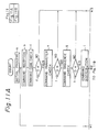
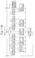
- FIG. 6 is a block diagram of an IC card system embodying the present invention.
- the characters "CC" denote a conventional communication controller
- 20 denotes an external IC card acceptance means provided with a conventional reader-writer for data communication with the IC card 10
- 26 a processor containing in particular a terminal EMAM, i.e. external memory access means
- a terminal station for example a personal computer 31 handling an application program (APL).
- APL application program
- a first logical system constituted by the CPU 4 and the external memory (EMEM) 11 is isolated from a second logical systemconstituted by the CPU 4 and the internal memory (IMEM) 5, although the first logical system and the second logical system can be logically connected together by the external IC card acceptance means 20 via the respective interfaces (27 and 3).
- the CPU 4 executes a program related to a device EMAM, and the IC card acceptance means (EIAM) 20, e.g. the reader-writer and reading and writing device, communicates with the CPU 4 and the EMEM 11.
- EIAM IC card acceptance means
- the processor (CPU) 26 executes a program related to a terminal EMAM.
- the CPU (terminal EMAM) 26 is supplied with a command by the aforesaid application program (APL), and in accordance with the kind of command, the CPU 26 selectively executes an internal processing of the terminal EMAM, an access to the external memory 11, and an access to the CPU 4 (device EMAM), and according to the result of this internal processing and the result of the access, an appropriate response is returned to a personal computer 31 (application program).
- APL application program
- the CPU 4 (device EMAM), after recognition by the terminal EMAM 26 of a command from the application program, is called by the terminal EMAM 26, if required by the resultant recognition and the CPU 4 then executes a command given by the terminal EMAM. The result of this command execution is returned to the terminal EMAM.
- FIG. 7 is a block diagram showing the principles of construction of an IC card of a system embodying the invention.
- the IC card of Fig. 7 is designed while taking security into consideration.
- the IC card 10 having a security function is comprised of the aforesaid external memory (EMEM) 11, an address holding means 44 for holding addresses of the files 19 stored in the EMEM 11, a cryptograph management information memory means 45 for storing the cryptographic management information used for enciphering data and for deciphering the ciphered data, a write processing means 43, a first read processing means 41 and a second read processing means 42.
- the means 41, 42 and 43 are functions of the CPU 4, and the means 44 and 45 are realized by the internal memory (IMEM) 5, e.g., a main memory.
- IMEM internal memory
- the write processing means 43 is able to start operating upon receipt of a write command WC and the corresponding write data WD, encipher the thus given write data WD with reference to the cryptograph management information, search the corresponding address AD of the external memory (EMEM) 11 at which the thus enciphered write data CWD is to be written by referring to the address holding means 44, and to return the enciphered write data CWD and the corresponding address AD, as a response.
- EMEM external memory
- the first read processing means 41 is able to start operating upon receipt of a first read command RC1 and the corresponding file number FN of the file 19, to search the corresponding read address RA specified by the given file number with reference to the address holding means 44, and to return the read address RA as a response.
- the second read processing means 42 is able to start operating upon receipt of a second read command RC 2 and a ciphered read data CRD, to decipher the thus given enciphered read data CRD by referring to the cryptographic management information, and to return the thus deciphered read data DRD as a response.
- the address holding means 44 is realized by the internal memory, and the address holding means specifies a new area in the file 9 with reference to a vacant area in the first directory 21.
- the means 45 (Fig. 7) has various keys and a ciphering algorithm, commonly known as a "DES” (Data Encription System proposed by IBM).
- DES Data Encription System proposed by IBM
- Figure 8 is a block diagram for clarifying a write process performed in an IC card of Fig. 7. For example, when writing data in the external memory (EMEM) 11, the following process is carried out:
- Figure 9 is a block diagram for clarifying a read process performed in an IC card of Fig. 7. For example, when reading data from the external memory (EMEM) 11, the following process is carried out:
- FIGS 10A and 10B display a general concept of a data processing system including an IC card of a system embodying the invention.
- Fig. 10A displays the side of the IC card 10
- Fig. 10B displays the side of the external IC card acceptance means 20 together with the terminal station 30, e.g., a personal computer.
- reference numeral 61 denotes a reset processing means
- 62 a personal identification number (PIN) verification processing means
- 63 a card authentication (AC) processing means
- 64 a file open processing means
- an E (abbreviation of EMEM 11) write 1 processing means 66 an E write 2 processing means
- 67 an E read 1 processing means 68 an E read 2 processing means
- 69 a file close processing means.
- C and R represent a command block and a response block, respectively.
- the internal memory e.g., a main memory (IMEM), 5 holds system directory/system information, PIN management information, card issuer identification (ID) management information, card AC management information, APL-ID management information, system AC management information, cryptograph management information, i.e., keys for drafting a cryptograph or deciphering the cryptograph, an EMAM (external memory access means) directory, external memory (EMEM) management files, and so on.
- the personal identification number (PIN) is a secret code for confirming whether or not the user of the IC card is an entitled user. The PIN is registered in the IC card and, when the IC card is used, the PIN is checked for verification with the secret code input by a user.
- the IC card is not activated until the PIN verification is satisfied, whereby the IC card is able to access the system (20, 30).
- PIN's exist, such as a card manufacturer PIN, a transport PIN, card issuer PIN, an own PIN, and so on.
- the card issuer ID management information is, for example, a name of a bank, a bank code, a card issuing date, a card issuance number, and so on.
- the authentication code (AC) is composed of data or an algorithm, in terms of elements (user, card, terminal machine or terminal station, service provider and the like) comprising an IC card system, used for confirming an authentication between any two elements.
- the APL-ID is a key essential to a business file when accessed by a business application program. Namely, a business application is made possible by specifying the APL-ID, to allow access to a required business file without referring to a physical address, and so on.
- the cryptograph management information produces a cryptograph for deciphering the ciphered data stored in the external memory (EMEM) 11 and a management information of a radix number required when a new data is to be stored therein, and as materials similar thereto, a file correspondence number of the files in the EMEM 11, a cryptograph for deciphering, data which has been cryptographically processed, and so on.
- the EMAM (external memory access means) directory is composed of a directory for the EMEM 11 and a directory for the internal memory (IMEM) 5.
- the directory for the EMEM 11 manages file names for managing the EMEM 11, and file correspondence numbers for managing the same.
- the directory for the IMEM 5 manages a file correspondence number in the external memory (EMEM) 11 and addresses in a memory, managing attribute information with regard to the files in the EMEM 11.
- the EMEM management serves as an area for managing, in the file units, the attribute information for data in each file of the EMEM 11, which attribute information is managed by the directory for the IMEM.
- attribute information is recorded which relates to the data in each file of the EMEM 11. Further similar contents to be managed exist, such as the date of drafting of the related files, renewal date, and start and end of each physical address corresponding to the external memory (EMEM) 11.
- the EMAM (external memory access means) 23 is provided with the above mentioned processing means 61 through 69 and others.
- the reset processing means 61 starts operating upon receipt of a RESET command from the side 20, 30 (Fig. 10B) and resets the system directory and the system information in the internal memory (IMEM) 5 (Fig. 10A), and then sends a RESET response to the side 20, 30.
- the PIN verification processing means 62 starts operating upon receipt of a PIN verification command accompanied by PIN data and carries out a verification process of the PIN data with reference to the PIN management information (Fig. 10A), and then sends a verification result to the side 20, 30.
- the card AC processing means 63 (Fig.
- the file open processing means 64 starts operating upon receipt of a file open command and carries out a check of an access right with reference to the system AC management information in the IMEM 5 (Fig. 10A), and then sends the result of the related file open to the side 20, 30.
- the E write 1 processing means 65 starts operating upon receipt of an E write 1 command and the corresponding data, enciphers the thus given data, and returns the enciphered data and a write position.
- the above write position is a write position in the external memory (EMEM) 11, and is obtained by reference to the content of the EMEM management file in the IMEM 5 (FIG. 10A).
- the E write 2 processing means 66 starts operating upon receipt of an E write 2 command and resultant information (the result of a write operation to the EMEM 11), and writes the result of the write operation to the EMEM 11 for the EMEM management file in the IMEM 5 (Fig. 10A), and then sends the result of the related process to the side 20, 30.
- the E read 1 processing means 67 starts operating upon receipt of the E read 1 command and a file name, and searches for a position on the external memory (EMAM) 11 in which the related file is stored, with reference to the EMEM management file, and then sends the result and the position to the side 20, 30 (Fig. 10B).
- the EMAM read 2 processing means 68 starts operating upon receipt of an E read 2 command and enciphered data and carried out a deciphering operation with reference to the cryptograph management information in the IMEM 5 (Fig. 10A), and then sends the result and the deciphered data to the side 20, 30 (Fig. 10B).
- the file close processing means 69 starts operating upon receipt of a file close command and carries out a file close operation, and then sends the result to the side 20, 30 (Fig. 10B).
- the terminal when the IC card 10 is inserted in the reader-writer, together with the reading and writing device, the terminal, i.e., the external IC card acceptance means 20, sends a RESET command to the IC card 10.
- the means 20 issues a PIN verification request, a card AC request, a file open request, and a E write 1 request, and thereafter, the related write operation to the EMEM 11 is performed and the E write 2 request is issued.
- the means 20 issues an E read 1 request, and thereafter, the related read operation to the EMEM 11 is carried out. Then an E read 2 request is issued, and when the access to the EMEM 11 is completed, a file close request is issued.
- a PIN command is sent to the processor (CPU) 4 forming the processing means 61 through 69; when a card AC request is issued, a card AC command is sent to the CPU 4 in the IC card 10; when a file open request is issued, a file open command is sent to the CPU 4 in the IC card 10; when an E write 1 request is issued, an E write 1 command is sent to the CPU 4 in the IC card 10; when an E write 2 request is issued, an E write 2 command is sent to the CPU 4 in the IC card 10; when an E read 1 request is issued, an E read 1 command is sent to the CPU 4 in the IC card 10; and when an E read 2 request is issued, an E read 2 command is sent to the CPU 4 in the IC card 10.
- FIGs 11A and 11B are flow charts of a process for each command, performed by a CPU in an IC card of a system embodying the invention.
- An initial process is started ("a") by a power-ON, and when a command is received ("b") from a PIN PAD (Fig. 10B), a command check is carried out ("c"). If the command code is correct (YES in step “d"), a command parameter check is carried out ("e”). The command parameter check determines whether or not the attribute information conforms with the prescribed parameter. If the result at step “d” is NO, an error response is edited in step "K” in Fig. 11B, and an error response is sent to the means 20 ("L” in Fig. 11B).
- step "f" If the result of the command parameter check is correct (YES in step "f"), a command sequence check is started ("g"). If the result at step “f” is NO, the error response edit is carried out. If the result of the command sequence check is YES ("h"), a command distribution is started ("i"). The command sequence check is introduced to find contradictions in the command sequence; for example, if a file write command precedes a file open command, this is a contradiction. If the result of the command c sequence check is NO in step “h”, the flow goes to step “K” (Fig. 11B). When one of the various processes is finished, a response is sent to the means 20 ("L” in Fig. 11B). The above mentioned processes are performed in steps “A” through “J” in Fig. 11B. Note, for brevity, in some of these steps the reference character “E” represents the "EMEM”, i.e., the external memory 11 (Fig. 5 and others). Details of these processes will be presented below.
- E represents
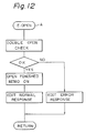
- FIG 12 is a detailed flow chart of the process "A" shown in Fig. 11B.
- E OPEN process "A” a double open check is carried out to avoid a double occupation of the same file. If the result is YES, an open finished memo (flag) is made ON (hoist), and a normal response is edited. In the result is NO, an error response is edited.
- FIG 13 is a detailed flow chart of the process "B" shown in Fig. 11B.
- E CLOSE process "B” a double close check is carried out for a similar reason as for the double open check, and if the result is YES or NO, a normal or an error response is edited accordingly.
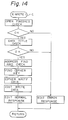
- Figure 14 is a detailed flow chart of the process "C" shown in Fig. 11B.
- E WRITE 1 process "C” it is determined whether or not the related data is open. If the result is YES, a data title check is carried out to determine whether or not the related data has a right to access the file. If the result is YES, the corresponding address is found and edited. Further, the corresponding key is found, and using the key, the write data is enciphered, and then edited. Finally, the related edition of the response is performed. If the result of the step (OPEN FINISHED CHECK) is NO, the related edition of the response is performed. This also applies when the result of the data title check is NO.
- FIG 15 is a detailed flow chart of the process "D" shown in Fig. 11B.
- E WRITE 2 an E write finished check is carried out. Namely, it is determined whether or not the preceding E write 1 process was completed without error. If the result is YES, the resultant information is checked. The resultant information indicates, for example, whether or not an overwrite has occurred in the external memory (EMEM). If the result of the check is NO, the error response is edited. If the check of the resultant information indicates a normal result, then a normal completion of the write process is recorded (memo). If the check indicates an abnormal result, then an abnormal completion of the write process is recorded (memo). The normal response is then edited, wherein the term "normal” means that the flow per se was completed normally and is not concerned with the above mentioned abnormal completion of the write process.
- EMEM external memory
- FIG 16 is a detailed flow chart of the process "E" shown in Fig. 11B.
- the open finish check is carried out as in the flow of Fig. 14. If the result of the check is YES, a data title check is started, as in the flow of Fig. 14. If the result of the check is YES, the corresponding address is found by the address holding means (shown by 44 in Fig. 7), as in the flow of Fig. 14, and then edited. The remaining steps are similar to those explained before.
- FIG 17 is a detailed flow chart of the process "F" shown in Fig. 11B.
- the E read 1 finished check is carried out in the same as the corresponding step in Fig. 15. If the result is YES, the corresponding cipher key is found, and using the key, the read data is deciphered to edit the read data. The remaining steps are similar to those explained before.
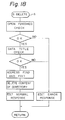
- Figure 18 is a detailed flow chart of the process "G" shown in Fig. 11B.
- E DELETE E DELETE
- an open finished check is carried out, and if the result of the check is YES, a data title check is carried out. Namely, if the result of this check is YES, the corresponding address is found and edited to delete the content of the directory (shown by 21 in Fig. 5). The remaining steps are similar to those explained before.
- FIG. 9 is a detailed flow chart of the process "H" shown in Fig. 11B.
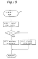
- VERIFY PIN process an authentication check for an input PIN data is carried out. The remaining steps are similar to those explained before.
- FIG 20 is a detailed flow chart of the process "I" shown in Figure 11B.
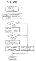
- a validity check for the system information directory is carried out, and if the result of the check is YES, then a validity of the CREATE is checked. Namely, if the result of this check is YES, a file registration is carried out. The remaining steps are the same as described previously. The vality of the CREATE is checked to confirm whether the file is created as required. If the result of the vality check is YES, the registration of the file to be created is carried out. The remaining steps are similar to those explained before.
- Figure 21 is a detailed flow chart of the process "J" shown in Fig. 11B.
- the directory for the newly introduced file is created. Namely, first double registration is checked to avoid a registration conflict. If the result of the check is YES, then it is determined whether or not a sufficient directory area exists. If the result of the check is YES, a registration to the directory is carried out. The remaining steps are similar to those explained before.
- the IC card 10 is provided, as one body with the external memory (EMEM) 11, which has a very large memory capacity, and therefore, it is possible to store a vast amount of information, for example, video information. Specifically, it is possible to record, for example, a photograph of the user's face, user'a voice, user's signature, user's fingerprints, and so on. Of course, it is also possible to store information which overflows the internal memory (IMEM) 5 having a small memory capacity. In this case, the date must be recorded simultaneously, since such information, for example, a photograph of the user's face, will not represent the user's face after an elapse of time. Accordingly, the date of the record is also important for, for example, a driving licence, a passport, and the like.
- EMEM external memory
- a memory history management area can be created.
- the memory history management area manages information to be stored in the external memory (EMEM) 11, such as a photograph of the user's face and so on, as mentioned above.
- EMEM external memory
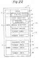
- FIG 22 is a schematic diagram of the general construction of devices mounted in and on an IC card, in particular a memory history management part according to an embodiment of the invention.
- the history management part 70 is composed of at least a memory history directory 71 formed in the first directory 21 (Fig. 5).
- the memory history directory 71 preferably cooperates with a history record area 72 formed in the second files, i.e., the file 9 (Fig. 5).
- the history directory 71 and the record area 72 are controlled by the processor (CPU) 4, in particular the external memory access means (EMAM) 23.
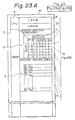
- Figures 23A and 23B show a specific arrangement of a memory history management part shown in Fig. 22.
- the data files in the external memory may be used with a regulated format as shown by 11 in Fig. 23B or a free format a shown by 11′.
- 11′ (left side in Fig. 23B) is regulated with a plurality of blocks, such as B1 , B2 --- B n .
- block B1 is allotted to the photograph data, B2 to the voice data, B3 to the fingerprint data, B4 to the signature data, and B5 to the overflow data from the internal memory (IMEM) 5.
- Each of the blocks B1 through B n is composed of a plurality of sections S1 through S m .
- the internal memory (IMEM) 5 contains therein the memory history directory 71 and the history record area 72, as the memory history management part 70 (Fig. 22).
- the memory history directory 71 indicates physical addresses on the external memory (EMEM) 11.
- the history record area 72 is divided with a plurality of rows, and each row is predefined by both block numbers B1 , B2 --- B n and section numbers S1 , S2 --- S m . Therefore, each time a write operation to the blocks B1 through B n of Fig. 23B is carried out, the date on which the related write operation was made is recorded in the corresponding row of the history record area 72. (Fig. 23A).
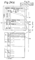
- Figures 24A and 24B are a flow chart of the read and write operations to an external memory (EMEM), and also depict an arrangement of the related memories.
- the content of Fig. 24A is substantially the same as the content shown in Figs. 23A and 23B.
- the processing flow of Fig. 24B is programmed in the external memory access means (EMAM) 23 in Fig. 23A and the program is executed by the external IC card acceptance means 20 (terminal machine) and, if necessary, the terminal station 30.
- the communication is handled by the reader-writer and the reading and writing device.
- a read operation is started by the processor (CPU) 4 in the IC card 10 (refer to "a" in Fig. 24B).
- This command is a request to scan the history, and thus a corresponding search in the history directory 71 is carried out ("b") and the physical address corresponding to the searched logical address is found.
- data is read from the EMEM 11 by the acceptance means 20 ("c"), and thereafter, the date on which the related read operation was carried out is written in the history directory 71 by the CPU 4 ("d").
- the thus read data is sent to a demander of the related read request, e.g., the terminal station 30, by the acceptance means 20 ("e").
- the CPU 4 When a write command, the corresponding physical address, and the corresponding write data are received by the CPU 4 ("f"), the CPU 4 (Fig. 23A) carries out a search of the history directory 71 using the given logical address, to find the corresponding physical address ("g"). Based on the found physical address, the related write operation is carried out by the acceptance means 20 ("h"), and thereafter, the date on which the write operation was carried out is recorded by the CPU 4 ("i"). The result of the write operation is sent to the demander of the relate write request, e.g., the terminal station 30, by the acceptance means 20 ("j").
- an IC card of a system embodying the invention can handle a vast amount of data compared to the conventional IC card 1.
- the external memory (EMEM) is exposed outside the body of the IC card, security for the data stored therein can be assured because the EMEM is governed by the internal CPU alone.
Abstract
Description
- The present invention relates to integrated circuit cards (hereinafter referred to as IC cards).
- The convenience of IC cards for multi-purpose usage, such as for banking, shopping, and travel services, etc., has encourages a widespread use of these cards, which although having different nomenclatures, for example, Smart Card or Chip-in Card, provide similar facilities.
- As explained in detail hereinafter, one form of prior art IC card contains a processor, i.e. a central processing unit (CPU) and a memory, both packaged in a plastic plate as one body. The capacity of the memory might typically be 8K bytes, but such memory capacity may not be sufficient when the facilities provided by the IC card are to be expanded. If a large capacity memory is required, a laser memory card may be provided separately. A laser memory card has a memory which can be written and read by laser light. The capacity of the laser card can be several million bytes. In the known art, however, such a laser card is physically and logically separated from the IC card.
- As a result, the laser memory can be used only when a special external terminal machine, i.e. a special card acceptance means, is available, and this, of course, is inconvenient.
- An alternative form of IC card system has been considered, having a magnetic stripe thereon, in which information recorded on the magnetic stripe is read and handled by a processor separate from the internal processor of the IC card. In such a system, the internal processor only reads and handles information stored in an internal memory of the card.
- In an embodiment of the present invention, the IC card is provided with an internal processor (CPU) which includes communication means for controlling an external auxiliary memory, provided integrally with the body of the IC card, by an external card acceptance means.
- An IC card system embodying the present invention desirably provides protection against illegal access to information in the external memory, and can advantageously provide an IC card system in which records relating to past access to information recorded in the external memory (update history) can be easily obtained by an authorised user after verification.
- Reference will now be made, by way of example, to the accompanying drawings, in which:
- Figure 1 is a perspective view of a conventional IC card;
- Figure 2 is a schematic diagram of the internal construction of an integrated circuit module;
- Figure 3 is a perspective view of an IC card of a system embodying the present invention;
- Figure 4 is a schematic diagram of an arrangement of devices in an IC card of a system embodying the present invention;
- Figure 5 is a schematic diagram of the general construction of devices mounted on and in an IC card for a system embodying the present invention;
- Fig. 6 is a block diagram of an IC card system embodying to the present invention;
- Fig. 7 is a block diagram illustrating the principles of construction of an IC card for a sytem embodying the present invention;
- Fig. 8 is a block diagram for clarifying a write process performed in the IC card shown in Fig. 7;
- Fig. 9 is a block diagram for clarifying a read process performed in the IC card shown in Fig. 7;
- Figs. 10A and 10B display a general concept of a data processing system,including an IC card, embodying the present invention;
- Figs. 11A and 11B are flow charts of a process for each command, performed by a CPU in an IC card of a system embodying the present invention;
- Fig. 12 is a detailed flow chart of the process "A" shown in Fig. 11B;
- Fig. 13 is a detailed flow chart of the process "B" shown in Fig. 11B;
- Fig. 14 is a detailed flow chart of the process "C" shown in Fig. 11B;
- Fig. 15 is a detailed flow chart of the process "D" shown in Fig. 11B;
- Fig. 16 is a detailed flow chart of the process "E" shown in Fig. 11B;
- Fig. 17 is a detailed flow chart of the process "F" shown in Fig. 11B;
- Fig. 18 is a detailed flow chart of the process "G" shown in Fig. 11B;
- Fig. 19 is a detailed flow chart of the process "H" shown in Fig. 11B;
- Fig. 20 is a detailed flow chart of the process "I" shown in Fig. 11B;
- Fig. 21 is a detailed flow chart of the process "J" shown in Fig. 11B;
- Fig. 22 is a schematic diagram of the general construction of devices mounted in an on an IC card, particularly a memory history management part, of a system embodying the present invention;
- Figs. 23A and 23B show a specific arrangement of the memory history management part shown in Fig. 22; and
- Figs. 24A and 24B are flow chart of read and write operations at an external memory (EMEM), and show an arrangement of related memories.
- Figure 1 is a perspective view of a conventional IC card. In Fig. 1,
reference 1 represents an IC card. TheIC card 1 contains anintegrated circuit module 2 comprising a processor (CPU) and an internal memory (neither of which are shown). The CPU and the memory transmit and receive data to and from external card acceptance means via a plurality ofcontacts 3. Figure 1 shows the rear surface of the IC card; the front surface thereof has a variety of devices mounted thereon, such as a display unit, a ten key unit, and so on. - Figure 2 is a schematic diagram of an internal construction of an integrated circuit module. The main components of the
integrated circuit module 2 are the processor (CPU) 4 and the internal memory (IMEM) 5. TheCPU 4 forms an IC card access means 6 and the memory, generally a main memory, forms a plurality offormat areas 8; theseformat areas 8 also define afile 9. - The internal memory access means (IMAM) 6 sets up an operating system and is able to process an access of the
IC card 1 to the external IC card acceptance means. When the access is directed to thefile 9 in thememory 5, a search is first made of thedirectory 7, which is a dictionary storing file numbers (Nos.). - In Fig. 2, the memory (IMEM) comprises an IC memory, for example, an electronically erasable programmable read only memory (EEPROM). The capacity of the IC memory might typically be 8 K bytes. As previously mentioned, such a memory capacity is not sufficient to develop a versatile general-purpose IC card, and accordingly, in the prior art, a laser memory card may be used an an accessory to the IC card. However, it is inconvenient to utilize a laser memory card with an IC card, despite the very large memory capacity of the laser memory card.
- In Figure 3, an IC card of a system embodying the present invention is provided with an
external memory 11 mounted on the surface of the body of theIC card 20 to form a monolithic structure. Theexternal memory 11 is adhered to the body of theIC card 20. As such, theexternal memory 11 is physically and logically separated from theintegrated circuit module 12. - Figure 4 is a schematic diagram of an arrangement of devices in an IC card of a system embodying the present invention. The
IC card 20 contains the processor (CPU) 4 and the internal memory (IMEM) 5, i.e. a main memory, both formed as theintegrated circuit module 12, i.e., an IC chip. The contacts (shown by 3 in Fig. 3 but not illustrated in Fig. 4) are used for data communication between theprocessor 4, together with theinternal memory 5, and the external IC card acceptance means. The external memory (EMEM) 11 does not perform data communication via thecontacts 3, but communicates directly with the external IC card acceptance means, as illustrated by a two-way arrow in Fig. 4. Accordingly, only theCPU 4 can manage theexternal memory 11. Note, identical components are represented by the same reference numerals or characters throughout the drawings. - Figure 5 is a schematic diagram of the general construction of devices mounted on and in an IC card of a system embodying to the present invention. The processor (CPU) 4 is usually provided with a program ROM which creates therein the internal memory access means (IMAM) 6 and the external memory access means (EMAM) 23 of the present invention. Namely, the means (IMAM) 6 and the means (EMAM) 23 are actually established as programs.
- The internal memory (IMEM) 5 is preferably a non-volatile memory, such as an EEPROM, and has a
first directory 21 and asecond directory 22 formed therein. Thesecond directory 22 defines theformat areas 8 of thefile 9 allotted for the internal memory per se (main memory), and thus thesecond directory 22 is substantially the same as thedirectory 7 shown in Fig. 2. Thefirst directory 21, however, defines theformat areas 8 of thefile 9 allotted for theexternal memory 11. Theformat areas 8 and format areas 17 (explained below) store user data relating to the IC card owner. - The
external memory 11 is composed of apassword area 17 and theformat areas 18 setting up afile 19. The password in thearea 17 is used in an authentication check of theexternal memory 11 performed by the internal processor. - The external memory (EMEM) 11 can have a memory capacity much larger than that of the internal memory (IMEM) 5, and accordingly, the
external memory 11 is may be an optical memory, such as laser memory, a CD-ROM and the like, which usually have a memory capacity of several M bytes even though small in size. - Figure 6 is a block diagram of an IC card system embodying the present invention. In Fig. 6, the characters "CC" denote a conventional communication controller, 20 denotes an external IC card acceptance means provided with a conventional reader-writer for data communication with the
IC card interface 27, for example, an optical reading and writing device, 26 a processor containing in particular a terminal EMAM, i.e. external memory access means, and 30 a terminal station, for example apersonal computer 31 handling an application program (APL). - In Fig. 6, a first logical system constituted by the
CPU 4 and the external memory (EMEM) 11 is isolated from a second logical systemconstituted by theCPU 4 and the internal memory (IMEM) 5, although the first logical system and the second logical system can be logically connected together by the external IC card acceptance means 20 via the respective interfaces (27 and 3). Namely, only data handled by theCPU 4 is sent to the external memory (EMEM) 11, and read and write operations for the external memory are carried out by using only addresses determined by theCPU 4. TheCPU 4 executes a program related to a device EMAM, and the IC card acceptance means (EIAM) 20, e.g. the reader-writer and reading and writing device, communicates with theCPU 4 and theEMEM 11. In theEIAM 20, the processor (CPU) 26 executes a program related to a terminal EMAM. The CPU (terminal EMAM) 26 is supplied with a command by the aforesaid application program (APL), and in accordance with the kind of command, theCPU 26 selectively executes an internal processing of the terminal EMAM, an access to theexternal memory 11, and an access to the CPU 4 (device EMAM), and according to the result of this internal processing and the result of the access, an appropriate response is returned to a personal computer 31 (application program). The CPU 4 (device EMAM), after recognition by theterminal EMAM 26 of a command from the application program, is called by theterminal EMAM 26, if required by the resultant recognition and theCPU 4 then executes a command given by the terminal EMAM. The result of this command execution is returned to the terminal EMAM. - When using the
IC card 10, security must be taken into consideration, particular the security of data stored in the external memory (EMEM) 11. This is because, the contents of theEMEM 11 can be easily stolen by a third party, since theEMEM 11 is exposed outside the body of theIC card 10. - Figure 7 is a block diagram showing the principles of construction of an IC card of a system embodying the invention. The IC card of Fig. 7 is designed while taking security into consideration. In Fig. 7, the
IC card 10 having a security function is comprised of the aforesaid external memory (EMEM) 11, an address holding means 44 for holding addresses of thefiles 19 stored in theEMEM 11, a cryptograph management information memory means 45 for storing the cryptographic management information used for enciphering data and for deciphering the ciphered data, a write processing means 43, a first read processing means 41 and a second read processing means 42. The means 41, 42 and 43 are functions of theCPU 4, and themeans - The write processing means 43 is able to start operating upon receipt of a write command WC and the corresponding write data WD, encipher the thus given write data WD with reference to the cryptograph management information, search the corresponding address AD of the external memory (EMEM) 11 at which the thus enciphered write data CWD is to be written by referring to the address holding means 44, and to return the enciphered write data CWD and the corresponding address AD, as a response.
- The first read processing means 41 is able to start operating upon receipt of a first read command RC1 and the corresponding file number FN of the
file 19, to search the corresponding read address RA specified by the given file number with reference to the address holding means 44, and to return the read address RA as a response. - The second read processing means 42 is able to start operating upon receipt of a second
read command RC 2 and a ciphered read data CRD, to decipher the thus given enciphered read data CRD by referring to the cryptographic management information, and to return the thus deciphered read data DRD as a response. - The address holding means 44 is realized by the internal memory, and the address holding means specifies a new area in the
file 9 with reference to a vacant area in thefirst directory 21. - Note, the means 45 (Fig. 7) has various keys and a ciphering algorithm, commonly known as a "DES" (Data Encription System proposed by IBM).
- Figure 8 is a block diagram for clarifying a write process performed in an IC card of Fig. 7. For example, when writing data in the external memory (EMEM) 11, the following process is carried out:
- (I) the given write command WC and the corresponding write data WD are input to the
IC card 10, - (II) the enciphered write data CWD and the corresponding address AD for writing in the external memory (EMEM) 11 are obtained and output from the
IC card 10, and - (III) the thus enciphered write data CWD is written in the
EMEM 11. - Figure 9 is a block diagram for clarifying a read process performed in an IC card of Fig. 7. For example, when reading data from the external memory (EMEM) 11, the following process is carried out:
- (I) the given first read command RC1 and the corresponding file number FN are input in the
IC card 10, - (II) the corresponding read address AD for the
external memory 11 is searched by the address holding means 44 and output from theIC card 10, - (III) the enciphered read data CRD is obtained, by using the searched read address AD, from the
external memory 11, - (IV) the enciphered read data CRD from the
external memory 11 is given to theIC card 10 together with a second read command RC2, and - (V) a deciphered read data DRD is output from the IC card, in response to the second read command RC2.
- Figures 10A and 10B display a general concept of a data processing system including an IC card of a system embodying the invention. Fig. 10A displays the side of the
IC card 10 and Fig. 10B displays the side of the external IC card acceptance means 20 together with theterminal station 30, e.g., a personal computer. In Fig. 10A,reference numeral 61 denotes a reset processing means, 62 a personal identification number (PIN) verification processing means, 63 a card authentication (AC) processing means, 64 a file open processing means 65 an E (abbreviation of EMEM 11) write 1 processing means, 66 anE write 2 processing means, 67 an E read 1 processing means, 68 an E read 2 processing means, and 69 a file close processing means. Note, in Fig. 10B, C and R represent a command block and a response block, respectively. - The internal memory, e.g., a main memory (IMEM), 5 holds system directory/system information, PIN management information, card issuer identification (ID) management information, card AC management information, APL-ID management information, system AC management information, cryptograph management information, i.e., keys for drafting a cryptograph or deciphering the cryptograph, an EMAM (external memory access means) directory, external memory (EMEM) management files, and so on. The personal identification number (PIN) is a secret code for confirming whether or not the user of the IC card is an entitled user. The PIN is registered in the IC card and, when the IC card is used, the PIN is checked for verification with the secret code input by a user. The IC card is not activated until the PIN verification is satisfied, whereby the IC card is able to access the system (20, 30). A variety of PIN's exist, such as a card manufacturer PIN, a transport PIN, card issuer PIN, an own PIN, and so on. The card issuer ID management information is, for example, a name of a bank, a bank code, a card issuing date, a card issuance number, and so on. The authentication code (AC) is composed of data or an algorithm, in terms of elements (user, card, terminal machine or terminal station, service provider and the like) comprising an IC card system, used for confirming an authentication between any two elements. This data or algorithm is predetermined between two elements, and thereafter, must be kept secret from other parties. Use of the AC enables a prevention of non-authorized use or forgery of an IC card and tampering with data in the IC card, and the detection of unauthorized use, forgery, and tampering with data. The APL-ID is a key essential to a business file when accessed by a business application program. Namely, a business application is made possible by specifying the APL-ID, to allow access to a required business file without referring to a physical address, and so on. The cryptograph management information produces a cryptograph for deciphering the ciphered data stored in the external memory (EMEM) 11 and a management information of a radix number required when a new data is to be stored therein, and as materials similar thereto, a file correspondence number of the files in the
EMEM 11, a cryptograph for deciphering, data which has been cryptographically processed, and so on. The EMAM (external memory access means) directory is composed of a directory for the EMEM 11 and a directory for the internal memory (IMEM) 5. The directory for theEMEM 11 manages file names for managing theEMEM 11, and file correspondence numbers for managing the same. The directory for theIMEM 5 manages a file correspondence number in the external memory (EMEM) 11 and addresses in a memory, managing attribute information with regard to the files in theEMEM 11. The EMEM management serves as an area for managing, in the file units, the attribute information for data in each file of theEMEM 11, which attribute information is managed by the directory for the IMEM. In the data area of the files in the external memory (EMEM) 1, attribute information is recorded which relates to the data in each file of theEMEM 11. Further similar contents to be managed exist, such as the date of drafting of the related files, renewal date, and start and end of each physical address corresponding to the external memory (EMEM) 11. - The EMAM (external memory access means) 23 is provided with the above mentioned processing means 61 through 69 and others. The reset processing means 61 (Fig. 10A) starts operating upon receipt of a RESET command from the
side 20, 30 (Fig. 10B) and resets the system directory and the system information in the internal memory (IMEM) 5 (Fig. 10A), and then sends a RESET response to theside side side side E write 1 command and the corresponding data, enciphers the thus given data, and returns the enciphered data and a write position. The above write position is a write position in the external memory (EMEM) 11, and is obtained by reference to the content of the EMEM management file in the IMEM 5 (FIG. 10A). The E write 2 processing means 66 starts operating upon receipt of anE write 2 command and resultant information (the result of a write operation to the EMEM 11), and writes the result of the write operation to the EMEM 11 for the EMEM management file in the IMEM 5 (Fig. 10A), and then sends the result of the related process to theside side 20, 30 (Fig. 10B). The EMAM read 2 processing means 68 starts operating upon receipt of an E read 2 command and enciphered data and carried out a deciphering operation with reference to the cryptograph management information in the IMEM 5 (Fig. 10A), and then sends the result and the deciphered data to theside 20, 30 (Fig. 10B). The file close processing means 69 starts operating upon receipt of a file close command and carries out a file close operation, and then sends the result to theside 20, 30 (Fig. 10B). - In the
terminal side 20 and 30 (Fig. 10B), when theIC card 10 is inserted in the reader-writer, together with the reading and writing device, the terminal, i.e., the external IC card acceptance means 20, sends a RESET command to theIC card 10. Where data is to be written in the external memory (EMEM) 11, themeans 20 issues a PIN verification request, a card AC request, a file open request, and aE write 1 request, and thereafter, the related write operation to theEMEM 11 is performed and the E write 2 request is issued. Where data in theEMEM 11 is to be read, themeans 20 issues an E read 1 request, and thereafter, the related read operation to theEMEM 11 is carried out. Then an E read 2 request is issued, and when the access to theEMEM 11 is completed, a file close request is issued. - When a PIN verification request is issued, a PIN command is sent to the processor (CPU) 4 forming the processing means 61 through 69; when a card AC request is issued, a card AC command is sent to the
CPU 4 in theIC card 10; when a file open request is issued, a file open command is sent to theCPU 4 in theIC card 10; when anE write 1 request is issued, anE write 1 command is sent to theCPU 4 in theIC card 10; when anE write 2 request is issued, anE write 2 command is sent to theCPU 4 in theIC card 10; when an E read 1 request is issued, an E read 1 command is sent to theCPU 4 in theIC card 10; and when an E read 2 request is issued, an E read 2 command is sent to theCPU 4 in theIC card 10. - Figures 11A and 11B are flow charts of a process for each command, performed by a CPU in an IC card of a system embodying the invention. An initial process is started ("a") by a power-ON, and when a command is received ("b") from a PIN PAD (Fig. 10B), a command check is carried out ("c"). If the command code is correct (YES in step "d"), a command parameter check is carried out ("e"). The command parameter check determines whether or not the attribute information conforms with the prescribed parameter. If the result at step "d" is NO, an error response is edited in step "K" in Fig. 11B, and an error response is sent to the means 20 ("L" in Fig. 11B). If the result of the command parameter check is correct (YES in step "f"), a command sequence check is started ("g"). If the result at step "f" is NO, the error response edit is carried out. If the result of the command sequence check is YES ("h"), a command distribution is started ("i"). The command sequence check is introduced to find contradictions in the command sequence; for example, if a file write command precedes a file open command, this is a contradiction. If the result of the command c sequence check is NO in step "h", the flow goes to step "K" (Fig. 11B). When one of the various processes is finished, a response is sent to the means 20 ("L" in Fig. 11B). The above mentioned processes are performed in steps "A" through "J" in Fig. 11B. Note, for brevity, in some of these steps the reference character "E" represents the "EMEM", i.e., the external memory 11 (Fig. 5 and others). Details of these processes will be presented below.
- Figure 12 is a detailed flow chart of the process "A" shown in Fig. 11B. In the E OPEN process "A", a double open check is carried out to avoid a double occupation of the same file. If the result is YES, an open finished memo (flag) is made ON (hoist), and a normal response is edited. In the result is NO, an error response is edited.
- Figure 13 is a detailed flow chart of the process "B" shown in Fig. 11B. In the E CLOSE process "B", a double close check is carried out for a similar reason as for the double open check, and if the result is YES or NO, a normal or an error response is edited accordingly.
- Figure 14 is a detailed flow chart of the process "C" shown in Fig. 11B. In the
E WRITE 1 process "C", it is determined whether or not the related data is open. If the result is YES, a data title check is carried out to determine whether or not the related data has a right to access the file. If the result is YES, the corresponding address is found and edited. Further, the corresponding key is found, and using the key, the write data is enciphered, and then edited. Finally, the related edition of the response is performed. If the result of the step (OPEN FINISHED CHECK) is NO, the related edition of the response is performed. This also applies when the result of the data title check is NO. - Figure 15 is a detailed flow chart of the process "D" shown in Fig. 11B. In the
E WRITE 2 process, an E write finished check is carried out. Namely, it is determined whether or not the preceding E write 1 process was completed without error. If the result is YES, the resultant information is checked. The resultant information indicates, for example, whether or not an overwrite has occurred in the external memory (EMEM). If the result of the check is NO, the error response is edited. If the check of the resultant information indicates a normal result, then a normal completion of the write process is recorded (memo). If the check indicates an abnormal result, then an abnormal completion of the write process is recorded (memo). The normal response is then edited, wherein the term "normal" means that the flow per se was completed normally and is not concerned with the above mentioned abnormal completion of the write process. - Figure 16 is a detailed flow chart of the process "E" shown in Fig. 11B. In the
E READ 1 process, the open finish check is carried out as in the flow of Fig. 14. If the result of the check is YES, a data title check is started, as in the flow of Fig. 14. If the result of the check is YES, the corresponding address is found by the address holding means (shown by 44 in Fig. 7), as in the flow of Fig. 14, and then edited. The remaining steps are similar to those explained before. - Figure 17 is a detailed flow chart of the process "F" shown in Fig. 11B. In the
E READ 2 process, the E read 1 finished check is carried out in the same as the corresponding step in Fig. 15. If the result is YES, the corresponding cipher key is found, and using the key, the read data is deciphered to edit the read data. The remaining steps are similar to those explained before. - Figure 18 is a detailed flow chart of the process "G" shown in Fig. 11B. In the E DELETE process, an open finished check is carried out, and if the result of the check is YES, a data title check is carried out. Namely, if the result of this check is YES, the corresponding address is found and edited to delete the content of the directory (shown by 21 in Fig. 5). The remaining steps are similar to those explained before.
- Figure 9 is a detailed flow chart of the process "H" shown in Fig. 11B. In the VERIFY PIN process, an authentication check for an input PIN data is carried out. The remaining steps are similar to those explained before.
- Figure 20 is a detailed flow chart of the process "I" shown in Figure 11B. In the CREATE E FILE process, a validity check for the system information directory is carried out, and if the result of the check is YES, then a validity of the CREATE is checked. Namely, if the result of this check is YES, a file registration is carried out. The remaining steps are the same as described previously. The vality of the CREATE is checked to confirm whether the file is created as required. If the result of the vality check is YES, the registration of the file to be created is carried out. The remaining steps are similar to those explained before.
- Figure 21 is a detailed flow chart of the process "J" shown in Fig. 11B. In the CREATE E DIR process, the directory for the newly introduced file is created. Namely, first double registration is checked to avoid a registration conflict. If the result of the check is YES, then it is determined whether or not a sufficient directory area exists. If the result of the check is YES, a registration to the directory is carried out. The remaining steps are similar to those explained before.
- As understood from the above description, the
IC card 10 is provided, as one body with the external memory (EMEM) 11, which has a very large memory capacity, and therefore, it is possible to store a vast amount of information, for example, video information. Specifically, it is possible to record, for example, a photograph of the user's face, user'a voice, user's signature, user's fingerprints, and so on. Of course, it is also possible to store information which overflows the internal memory (IMEM) 5 having a small memory capacity. In this case, the date must be recorded simultaneously, since such information, for example, a photograph of the user's face, will not represent the user's face after an elapse of time. Accordingly, the date of the record is also important for, for example, a driving licence, a passport, and the like. - According to an embodiment of the present invention, a memory history management area can be created. The memory history management area manages information to be stored in the external memory (EMEM) 11, such as a photograph of the user's face and so on, as mentioned above.
- Figure 22 is a schematic diagram of the general construction of devices mounted in and on an IC card, in particular a memory history management part according to an embodiment of the invention. As is clear, the arrangement of Fig. 22 is a modification of the arrangement shown in Fig. 5, explained previously. The
history management part 70 is composed of at least amemory history directory 71 formed in the first directory 21 (Fig. 5). Thememory history directory 71 preferably cooperates with ahistory record area 72 formed in the second files, i.e., the file 9 (Fig. 5). Thehistory directory 71 and therecord area 72 are controlled by the processor (CPU) 4, in particular the external memory access means (EMAM) 23. - Figures 23A and 23B show a specific arrangement of a memory history management part shown in Fig. 22. The data files in the external memory may be used with a regulated format as shown by 11 in Fig. 23B or a free format a shown by 11′. In the external memory (EMEM) 11′ (left side in Fig. 23B) is regulated with a plurality of blocks, such as B₁ , B₂ --- Bn. In the example, block B₁ is allotted to the photograph data, B₂ to the voice data, B₃ to the fingerprint data, B₄ to the signature data, and B₅ to the overflow data from the internal memory (IMEM) 5. Each of the blocks B₁ through Bn is composed of a plurality of sections S₁ through Sm.
- On the other hand, as shown in Fig. 23A, the internal memory (IMEM) 5 contains therein the
memory history directory 71 and thehistory record area 72, as the memory history management part 70 (Fig. 22). Thememory history directory 71 indicates physical addresses on the external memory (EMEM) 11. Thehistory record area 72 is divided with a plurality of rows, and each row is predefined by both block numbers B₁ , B₂ --- Bn and section numbers S₁ , S₂ --- Sm. Therefore, each time a write operation to the blocks B₁ through Bn of Fig. 23B is carried out, the date on which the related write operation was made is recorded in the corresponding row of thehistory record area 72. (Fig. 23A). - Figures 24A and 24B are a flow chart of the read and write operations to an external memory (EMEM), and also depict an arrangement of the related memories. The content of Fig. 24A is substantially the same as the content shown in Figs. 23A and 23B. The processing flow of Fig. 24B is programmed in the external memory access means (EMAM) 23 in Fig. 23A and the program is executed by the external IC card acceptance means 20 (terminal machine) and, if necessary, the
terminal station 30. The communication is handled by the reader-writer and the reading and writing device. - When a read command and the corresponding logical address are sent from the acceptance means 20, a read operation is started by the processor (CPU) 4 in the IC card 10 (refer to "a" in Fig. 24B). This command is a request to scan the history, and thus a corresponding search in the
history directory 71 is carried out ("b") and the physical address corresponding to the searched logical address is found. Using the found physical address, data is read from the EMEM 11 by the acceptance means 20 ("c"), and thereafter, the date on which the related read operation was carried out is written in thehistory directory 71 by the CPU 4 ("d"). The thus read data is sent to a demander of the related read request, e.g., theterminal station 30, by the acceptance means 20 ("e"). - When a write command, the corresponding physical address, and the corresponding write data are received by the CPU 4 ("f"), the CPU 4 (Fig. 23A) carries out a search of the
history directory 71 using the given logical address, to find the corresponding physical address ("g"). Based on the found physical address, the related write operation is carried out by the acceptance means 20 ("h"), and thereafter, the date on which the write operation was carried out is recorded by the CPU 4 ("i"). The result of the write operation is sent to the demander of the relate write request, e.g., theterminal station 30, by the acceptance means 20 ("j"). - As explained above in detail, an IC card of a system embodying the invention can handle a vast amount of data compared to the
conventional IC card 1. Although the external memory (EMEM) is exposed outside the body of the IC card, security for the data stored therein can be assured because the EMEM is governed by the internal CPU alone.
Claims (30)
a processor contained therein and communicating with an external IC card acceptance means;
an internal memory contained therein and cooperating with the processor and forming data files;
an external memory mounted on a surface of a body of the IC card as one body; and
an external memory access means, other than an inherent internal memory access means, formed by said processor, which external memory access means alone can access said external memory by way of said external IC card acceptance means.
said write processing means starting operation upon receipt of a write command and the corresponding write data, enciphering the received write data with reference to the said cryptographic management information, searching the corresponding address of said external memory at which the enciphered write data is to be written with reference to said address holding means, and sending the enciphered write data and the corresponding address, as a response,
said first read processing means starting operation upon receipt of a first read command and a corresponding file number of said file in the external memory, searching the corresponding read address specified by the given file number with reference to said address holding means and sending the read address as a response,
said second read processing means starting operation upon receipt of a second read command and enciphered read data, deciphering the received enciphered read data with reference to said cryptographic management information, and sending the deciphered read data as a response.
Applications Claiming Priority (4)
| Application Number | Priority Date | Filing Date | Title |
|---|---|---|---|
| JP63038078A JP2534532B2 (en) | 1988-02-20 | 1988-02-20 | History management method |
| JP38078/88 | 1988-02-20 | ||
| JP154014/88 | 1988-06-22 | ||
| JP63154014A JPH025158A (en) | 1988-06-22 | 1988-06-22 | Expanded ic card and its accessing method |
Publications (3)
| Publication Number | Publication Date |
|---|---|
| EP0330404A2 true EP0330404A2 (en) | 1989-08-30 |
| EP0330404A3 EP0330404A3 (en) | 1991-02-06 |
| EP0330404B1 EP0330404B1 (en) | 1994-11-30 |
Family
ID=26377261
Family Applications (1)
| Application Number | Title | Priority Date | Filing Date |
|---|---|---|---|
| EP89301626A Revoked EP0330404B1 (en) | 1988-02-20 | 1989-02-20 | Integrated circuit cards |
Country Status (4)
| Country | Link |
|---|---|
| US (1) | US4985920A (en) |
| EP (1) | EP0330404B1 (en) |
| DE (1) | DE68919483T2 (en) |
| ES (1) | ES2064432T3 (en) |
Cited By (23)
| Publication number | Priority date | Publication date | Assignee | Title |
|---|---|---|---|---|
| FR2660465A1 (en) * | 1990-04-02 | 1991-10-04 | Gemplus Card Int | SECURITY CARD COMBINING A HIGH DENSITY STORAGE INFORMATION MEDIUM AND A MICROCIRCUIT, AND ITS USE IN A CARD READER. |
| EP0696016A2 (en) * | 1994-08-01 | 1996-02-07 | Fujitsu Limited | Method for managing security for card type storage medium and a card type storage medium |
| FR2732136A1 (en) * | 1995-03-06 | 1996-09-27 | Motorola Inc | DUAL ELECTRONIC CARD AND MANUFACTURING METHOD THEREOF |
| WO1997023846A1 (en) * | 1995-12-22 | 1997-07-03 | Italdata S.R.L. | A security system for the recognition of data, in particular personal identity data |
| EP0757337A3 (en) * | 1995-08-02 | 1999-09-15 | Bayer Ag | Unit, composed of data memory card and a reading/writing device |
| EP0945833A3 (en) * | 1998-03-26 | 1999-10-27 | Citicorp Development Center, Inc. | Method and system for remote banking with a multi-memory technology smart card |
| WO2000026866A1 (en) * | 1998-10-30 | 2000-05-11 | Motus Technologies Inc. | Secure memory expansion of an ic portable device |
| WO2002011081A1 (en) * | 2000-07-31 | 2002-02-07 | Orga Kartensysteme Gmbh | Data carrier comprising an optical memory |
| EP1079338A3 (en) * | 1999-08-27 | 2004-03-03 | Hitachi, Ltd. | Method of controlling information written into storage media |
| WO2004046935A2 (en) * | 2002-11-21 | 2004-06-03 | Philips Intellectual Property & Standards Gmbh | Circuit arrangement with non-volatile memory module and method of en-/decrypting data in the non-volatile memory module |
| US6840446B2 (en) | 1998-03-18 | 2005-01-11 | Citicorp Development Center, Inc. | Apparatus and system for optical card reading and method of use |
| EP1577782A1 (en) * | 2004-02-12 | 2005-09-21 | Irdeto Access B.V. | Method and system of external data storage |
| WO2006069194A3 (en) * | 2004-12-21 | 2006-11-23 | Sandisk Corp | Memory system with versatile content control |
| US7743409B2 (en) | 2005-07-08 | 2010-06-22 | Sandisk Corporation | Methods used in a mass storage device with automated credentials loading |
| US8051052B2 (en) | 2004-12-21 | 2011-11-01 | Sandisk Technologies Inc. | Method for creating control structure for versatile content control |
| US8140843B2 (en) | 2006-07-07 | 2012-03-20 | Sandisk Technologies Inc. | Content control method using certificate chains |
| US8245031B2 (en) | 2006-07-07 | 2012-08-14 | Sandisk Technologies Inc. | Content control method using certificate revocation lists |
| US8266711B2 (en) | 2006-07-07 | 2012-09-11 | Sandisk Technologies Inc. | Method for controlling information supplied from memory device |
| US8504849B2 (en) | 2004-12-21 | 2013-08-06 | Sandisk Technologies Inc. | Method for versatile content control |
| US8601283B2 (en) | 2004-12-21 | 2013-12-03 | Sandisk Technologies Inc. | Method for versatile content control with partitioning |
| US8613103B2 (en) | 2006-07-07 | 2013-12-17 | Sandisk Technologies Inc. | Content control method using versatile control structure |
| US8639939B2 (en) | 2006-07-07 | 2014-01-28 | Sandisk Technologies Inc. | Control method using identity objects |
| US9104618B2 (en) | 2008-12-18 | 2015-08-11 | Sandisk Technologies Inc. | Managing access to an address range in a storage device |
Families Citing this family (49)
| Publication number | Priority date | Publication date | Assignee | Title |
|---|---|---|---|---|
| JP2795855B2 (en) * | 1988-09-30 | 1998-09-10 | 株式会社東芝 | Image forming device |
| FR2654288B1 (en) * | 1989-11-08 | 1996-11-29 | Europ Rech Electr Lab | METHOD FOR AUTHENTICATING A MICROPROCESSOR CARD AND SYSTEM USING THE SAME. |
| US5663901A (en) | 1991-04-11 | 1997-09-02 | Sandisk Corporation | Computer memory cards using flash EEPROM integrated circuit chips and memory-controller systems |
| DE9109977U1 (en) * | 1991-08-12 | 1992-12-24 | Intelligent Solution Services Gmbh, 8051 Marzling, De | |
| SE470001B (en) * | 1991-09-12 | 1993-10-18 | Televerket | Procedure for identification and crypto exchange between two communicating devices for encrypted traffic |
| US6006297A (en) * | 1992-01-14 | 1999-12-21 | Gemplus Card International | Computer PC-card able to perform internal programs |
| WO2004077300A1 (en) * | 1992-01-22 | 2004-09-10 | Yoshimasa Kadooka | Ic memory card and protection therefor |
| US5448045A (en) * | 1992-02-26 | 1995-09-05 | Clark; Paul C. | System for protecting computers via intelligent tokens or smart cards |
| US5259025A (en) * | 1992-06-12 | 1993-11-02 | Audio Digitalimaging, Inc. | Method of verifying fake-proof video identification data |
| EP0583006B2 (en) * | 1992-08-13 | 2006-11-29 | Matsushita Electric Industrial Co., Ltd. | IC card with hierarchical file structure |
| US5293424A (en) * | 1992-10-14 | 1994-03-08 | Bull Hn Information Systems Inc. | Secure memory card |
| JP3471842B2 (en) * | 1993-03-29 | 2003-12-02 | 株式会社東芝 | Data management device, data storage device, and data management method |
| FR2717931B1 (en) * | 1994-03-23 | 1996-05-31 | Gemplus Card Int | Identity verification system. |
| CA2230230C (en) * | 1994-08-25 | 2006-08-15 | Geefield Pty. Ltd. | Method and apparatus for providing identification |
| KR0127029B1 (en) * | 1994-10-27 | 1998-04-01 | 김광호 | Memory card and recording, reproducing, and erasing method thereof |
| US5835689A (en) * | 1995-12-19 | 1998-11-10 | Pitney Bowes Inc. | Transaction evidencing system and method including post printing and batch processing |
| US6157919A (en) * | 1995-12-19 | 2000-12-05 | Pitney Bowes Inc. | PC-based open metering system and method |
| EP0818761A1 (en) * | 1996-07-12 | 1998-01-14 | Koninklijke KPN N.V. | Integrated circuit card, secure application module, system comprising a secure application module and a terminal and a method for controlling service actions to be carried out by the secure application module on the integrated circuit card |
| US6111506A (en) * | 1996-10-15 | 2000-08-29 | Iris Corporation Berhad | Method of making an improved security identification document including contactless communication insert unit |
| DE19648912B4 (en) * | 1996-11-26 | 2016-10-20 | Ipcom Gmbh & Co. Kg | Method and electrical device for data exchange and chip card for carrying out the method |
| US6199128B1 (en) * | 1998-03-26 | 2001-03-06 | Gemplus, S.C.A. | Smart card system for use with peripheral devices |
| US6315195B1 (en) * | 1998-04-17 | 2001-11-13 | Diebold, Incorporated | Transaction apparatus and method |
| US6567915B1 (en) * | 1998-10-23 | 2003-05-20 | Microsoft Corporation | Integrated circuit card with identity authentication table and authorization tables defining access rights based on Boolean expressions of authenticated identities |
| US6279114B1 (en) | 1998-11-04 | 2001-08-21 | Sandisk Corporation | Voltage negotiation in a single host multiple cards system |
| US6901457B1 (en) | 1998-11-04 | 2005-05-31 | Sandisk Corporation | Multiple mode communications system |
| US6341325B2 (en) * | 1999-01-12 | 2002-01-22 | International Business Machines Corporation | Method and apparatus for addressing main memory contents including a directory structure in a computer system |
| US6974938B1 (en) * | 2000-03-08 | 2005-12-13 | Tibotec Bvba | Microscope having a stable autofocusing apparatus |
| US7305104B2 (en) * | 2000-04-21 | 2007-12-04 | Digimarc Corporation | Authentication of identification documents using digital watermarks |
| CN1265330C (en) * | 2000-06-28 | 2006-07-19 | G·控股有限公司 | Transaction system with portable personal device for transaction identification and control |
| US20020128981A1 (en) * | 2000-12-28 | 2002-09-12 | Kawan Joseph C. | Method and system for facilitating secure customer financial transactions over an open network |
| WO2002075674A2 (en) * | 2001-03-16 | 2002-09-26 | G. Holdings Ltd. | System and method for replacing identification data on a portable transaction device |
| JP4899248B2 (en) * | 2001-04-02 | 2012-03-21 | 富士通セミコンダクター株式会社 | Semiconductor integrated circuit |
| WO2003003194A1 (en) * | 2001-06-27 | 2003-01-09 | Sony Corporation | Integrated circuit device, information processing device, information recording device memory management method, mobile terminal device, semiconductor integrated circuit device, and communication method using mobile terminal device |
| US7580408B2 (en) * | 2001-11-21 | 2009-08-25 | Alcatel Lucent | Configurable packet processor |
| US6845908B2 (en) * | 2002-03-18 | 2005-01-25 | Hitachi Semiconductor (America) Inc. | Storage card with integral file system, access control and cryptographic support |
| JP4027776B2 (en) * | 2002-10-25 | 2007-12-26 | 有限会社クリプトソフトウエア | Data processing system, processing apparatus and computer program |
| US6980087B2 (en) * | 2003-06-04 | 2005-12-27 | Pitney Bowes Inc. | Reusable electronic tag for secure data accumulation |
| US20060130154A1 (en) * | 2004-11-30 | 2006-06-15 | Wai Lam | Method and system for protecting and verifying stored data |
| GB0511599D0 (en) * | 2005-06-07 | 2005-07-13 | Ecebs Group Ltd | ITSO FCV2 application monitor |
| JP5439236B2 (en) * | 2010-03-12 | 2014-03-12 | 株式会社日立製作所 | Computer system and method of executing application program |
| USD729808S1 (en) | 2013-03-13 | 2015-05-19 | Nagrastar Llc | Smart card interface |
| USD759022S1 (en) | 2013-03-13 | 2016-06-14 | Nagrastar Llc | Smart card interface |
| US9888283B2 (en) | 2013-03-13 | 2018-02-06 | Nagrastar Llc | Systems and methods for performing transport I/O |
| USD758372S1 (en) * | 2013-03-13 | 2016-06-07 | Nagrastar Llc | Smart card interface |
| US9647997B2 (en) | 2013-03-13 | 2017-05-09 | Nagrastar, Llc | USB interface for performing transport I/O |
| USD780763S1 (en) | 2015-03-20 | 2017-03-07 | Nagrastar Llc | Smart card interface |
| USD864968S1 (en) | 2015-04-30 | 2019-10-29 | Echostar Technologies L.L.C. | Smart card interface |
| JP1647727S (en) * | 2018-02-01 | 2019-12-09 | ||
| USD930000S1 (en) | 2018-10-12 | 2021-09-07 | Huawei Technologies Co., Ltd. | Memory card |
Citations (2)
| Publication number | Priority date | Publication date | Assignee | Title |
|---|---|---|---|---|
| EP0138219A2 (en) * | 1983-10-17 | 1985-04-24 | Kabushiki Kaisha Toshiba | Method of storing encrypted data on a card |
| EP0147337A2 (en) * | 1983-12-30 | 1985-07-03 | Bull S.A. | Method and system for confidentially processing information registered on a portable carrier recording track with optical reading |
Family Cites Families (7)
| Publication number | Priority date | Publication date | Assignee | Title |
|---|---|---|---|---|
| US4529870A (en) * | 1980-03-10 | 1985-07-16 | David Chaum | Cryptographic identification, financial transaction, and credential device |
| JPS59100981A (en) * | 1982-12-01 | 1984-06-11 | Hitachi Ltd | Injustice preventing system for automatic cash transaction system |
| JPS6065388A (en) * | 1983-09-19 | 1985-04-15 | Toshiba Corp | Recording and reproducing system of information recording medium |
| US4575621A (en) * | 1984-03-07 | 1986-03-11 | Corpra Research, Inc. | Portable electronic transaction device and system therefor |
| JPH0670818B2 (en) * | 1984-09-07 | 1994-09-07 | カシオ計算機株式会社 | Verification card and its authentication method |
| DE3682476D1 (en) * | 1985-10-07 | 1991-12-19 | Toshiba Kawasaki Kk | PORTABLE ELECTRONIC DEVICE. |
| JPS62251991A (en) * | 1986-04-25 | 1987-11-02 | Fujitsu Ltd | File accessing system for ic card |
-
1989
- 1989-02-20 ES ES89301626T patent/ES2064432T3/en not_active Expired - Lifetime
- 1989-02-20 EP EP89301626A patent/EP0330404B1/en not_active Revoked
- 1989-02-20 DE DE68919483T patent/DE68919483T2/en not_active Revoked
- 1989-02-21 US US07/313,184 patent/US4985920A/en not_active Expired - Lifetime
Patent Citations (2)
| Publication number | Priority date | Publication date | Assignee | Title |
|---|---|---|---|---|
| EP0138219A2 (en) * | 1983-10-17 | 1985-04-24 | Kabushiki Kaisha Toshiba | Method of storing encrypted data on a card |
| EP0147337A2 (en) * | 1983-12-30 | 1985-07-03 | Bull S.A. | Method and system for confidentially processing information registered on a portable carrier recording track with optical reading |
Cited By (42)
| Publication number | Priority date | Publication date | Assignee | Title |
|---|---|---|---|---|
| EP0451024A1 (en) * | 1990-04-02 | 1991-10-09 | Gemplus Card International | Security card combining a high density information carrier and a microcircuit, and method for use in a card reader |
| FR2660465A1 (en) * | 1990-04-02 | 1991-10-04 | Gemplus Card Int | SECURITY CARD COMBINING A HIGH DENSITY STORAGE INFORMATION MEDIUM AND A MICROCIRCUIT, AND ITS USE IN A CARD READER. |
| EP0973125A3 (en) * | 1994-08-01 | 2000-02-23 | Fujitsu Limited | Method for managing security for card-type storage medium, and a card-type storage medium and a transaction apparatus therefor |
| EP0696016A2 (en) * | 1994-08-01 | 1996-02-07 | Fujitsu Limited | Method for managing security for card type storage medium and a card type storage medium |
| EP0696016A3 (en) * | 1994-08-01 | 1996-05-15 | Fujitsu Ltd | Method for managing security for card type storage medium and a card type storage medium |
| US5845069A (en) * | 1994-08-01 | 1998-12-01 | Fujitsu Limited | Card-type storage medium protecting data stored in its memory by interrupting an existing transaction after a predetermined permissible number of accesses |
| EP0973125A2 (en) * | 1994-08-01 | 2000-01-19 | Fujitsu Limited | Method for managing security for card-type storage medium, and a card-type storage medium and a transaction apparatus therefor |
| FR2732136A1 (en) * | 1995-03-06 | 1996-09-27 | Motorola Inc | DUAL ELECTRONIC CARD AND MANUFACTURING METHOD THEREOF |
| EP0757337A3 (en) * | 1995-08-02 | 1999-09-15 | Bayer Ag | Unit, composed of data memory card and a reading/writing device |
| US6244506B1 (en) | 1995-08-02 | 2001-06-12 | Bayer Aktiengesellschaft | Unit comprising data memory card and reading/writing device |
| WO1997023846A1 (en) * | 1995-12-22 | 1997-07-03 | Italdata S.R.L. | A security system for the recognition of data, in particular personal identity data |
| US6840446B2 (en) | 1998-03-18 | 2005-01-11 | Citicorp Development Center, Inc. | Apparatus and system for optical card reading and method of use |
| EP0945833A3 (en) * | 1998-03-26 | 1999-10-27 | Citicorp Development Center, Inc. | Method and system for remote banking with a multi-memory technology smart card |
| WO2000026866A1 (en) * | 1998-10-30 | 2000-05-11 | Motus Technologies Inc. | Secure memory expansion of an ic portable device |
| EP1079338A3 (en) * | 1999-08-27 | 2004-03-03 | Hitachi, Ltd. | Method of controlling information written into storage media |
| US7089388B1 (en) | 1999-08-27 | 2006-08-08 | Hitachi, Ltd. | Terminal for use in a system interfacing with storage media |
| US7330949B2 (en) | 1999-08-27 | 2008-02-12 | Hitachi, Ltd. | Terminal for use in a system interfacing with storage media |
| WO2002011081A1 (en) * | 2000-07-31 | 2002-02-07 | Orga Kartensysteme Gmbh | Data carrier comprising an optical memory |
| WO2004046935A2 (en) * | 2002-11-21 | 2004-06-03 | Philips Intellectual Property & Standards Gmbh | Circuit arrangement with non-volatile memory module and method of en-/decrypting data in the non-volatile memory module |
| WO2004046935A3 (en) * | 2002-11-21 | 2005-03-17 | Philips Intellectual Property | Circuit arrangement with non-volatile memory module and method of en-/decrypting data in the non-volatile memory module |
| US8155309B2 (en) | 2002-11-21 | 2012-04-10 | Eliposki Remote Ltd., L.L.C. | Circuit arrangement with non-volatile memory module and method for en-/decrypting data in the non-volatile memory module |
| CN100397284C (en) * | 2002-11-21 | 2008-06-25 | Nxp股份有限公司 | Circuit arrangement with non-volatile memory module and method of en-/decrypting data in the non-volatile memory module |
| US7395165B2 (en) | 2002-11-21 | 2008-07-01 | Nxp B.V. | Circuit arrangement with non-volatile memory module and method of en-/decrypting data in the non-volatile memory module |
| AU2005200555B2 (en) * | 2004-02-12 | 2010-12-02 | Irdeto Access B.V. | Method and system of external data storage |
| CN1655133B (en) * | 2004-02-12 | 2010-09-15 | 耶德托存取公司 | Method and system of external data storage |
| US7814269B2 (en) | 2004-02-12 | 2010-10-12 | Irdeto Access B.V. | Method and system of externalising / internalising a data record that allow processing of part or all of the record |
| EP1903444A1 (en) | 2004-02-12 | 2008-03-26 | Irdeto Access B.V. | Method and system of external data storage |
| EP1577782A1 (en) * | 2004-02-12 | 2005-09-21 | Irdeto Access B.V. | Method and system of external data storage |
| US8504849B2 (en) | 2004-12-21 | 2013-08-06 | Sandisk Technologies Inc. | Method for versatile content control |
| CN101120352B (en) * | 2004-12-21 | 2010-10-06 | 桑迪士克股份有限公司 | Method for protecting data stored in memory and device |
| WO2006069194A3 (en) * | 2004-12-21 | 2006-11-23 | Sandisk Corp | Memory system with versatile content control |
| US8051052B2 (en) | 2004-12-21 | 2011-11-01 | Sandisk Technologies Inc. | Method for creating control structure for versatile content control |
| US8601283B2 (en) | 2004-12-21 | 2013-12-03 | Sandisk Technologies Inc. | Method for versatile content control with partitioning |
| US7743409B2 (en) | 2005-07-08 | 2010-06-22 | Sandisk Corporation | Methods used in a mass storage device with automated credentials loading |
| US7748031B2 (en) | 2005-07-08 | 2010-06-29 | Sandisk Corporation | Mass storage device with automated credentials loading |
| US8220039B2 (en) | 2005-07-08 | 2012-07-10 | Sandisk Technologies Inc. | Mass storage device with automated credentials loading |
| US8140843B2 (en) | 2006-07-07 | 2012-03-20 | Sandisk Technologies Inc. | Content control method using certificate chains |
| US8266711B2 (en) | 2006-07-07 | 2012-09-11 | Sandisk Technologies Inc. | Method for controlling information supplied from memory device |
| US8245031B2 (en) | 2006-07-07 | 2012-08-14 | Sandisk Technologies Inc. | Content control method using certificate revocation lists |
| US8613103B2 (en) | 2006-07-07 | 2013-12-17 | Sandisk Technologies Inc. | Content control method using versatile control structure |
| US8639939B2 (en) | 2006-07-07 | 2014-01-28 | Sandisk Technologies Inc. | Control method using identity objects |
| US9104618B2 (en) | 2008-12-18 | 2015-08-11 | Sandisk Technologies Inc. | Managing access to an address range in a storage device |
Also Published As
| Publication number | Publication date |
|---|---|
| US4985920A (en) | 1991-01-15 |
| DE68919483T2 (en) | 1995-04-06 |
| DE68919483D1 (en) | 1995-01-12 |
| EP0330404A3 (en) | 1991-02-06 |
| EP0330404B1 (en) | 1994-11-30 |
| ES2064432T3 (en) | 1995-02-01 |
Similar Documents
| Publication | Publication Date | Title |
|---|---|---|
| EP0330404B1 (en) | Integrated circuit cards | |
| AU736325B2 (en) | Multi-application IC card system | |
| AU744984B2 (en) | Methods and apparatus for a travel-related multi-function smartcard | |
| US7702908B2 (en) | Tamper resistant module certification authority | |
| US6687800B1 (en) | Chip card comprising means and method for managing a virtual memory and associated communication method | |
| EP0985203A1 (en) | Key transformation unit for an ic card | |
| KR100349033B1 (en) | Storage medium having electronic circuit and method of managing the storage medium | |
| JPH021090A (en) | Ic card and method for writing its operation program | |
| JP2003058647A (en) | Memory rental service system of independent type identification device | |
| US5828053A (en) | Portable storage medium and portable storage medium issuing system | |
| KR20000069703A (en) | Chip card and method for its use | |
| JP3420761B2 (en) | A secure way to load multiple applications on a microprocessor memory card | |
| JP2003123032A (en) | Ic card terminal and individual authentication method | |
| JP2002304602A (en) | Card information update system | |
| JP3720113B2 (en) | Portable information storage medium, portable information storage medium system, and data access method for portable information storage medium | |
| JPH09265254A (en) | Mutual authentication system for information recording medium | |
| JPH025158A (en) | Expanded ic card and its accessing method | |
| JP2000508101A (en) | Chip card and usage of chip card | |
| JPH1069434A (en) | Ic card | |
| KR100520498B1 (en) | Method and Apparatus of issuing Storage Medium for Authentication, and Authentication Method and Apparatus using the Storage Medium | |
| JP2004086804A (en) | Ic card and ic card issuance system | |
| JP4295561B2 (en) | Card ticketing system | |
| US20030056106A1 (en) | Encryption system for preventing data from being copied illegally and method of the same | |
| JPS63278188A (en) | Ic card device | |
| KR100966824B1 (en) | Card issuing system and card issuing method |
Legal Events
| Date | Code | Title | Description |
|---|---|---|---|
| PUAI | Public reference made under article 153(3) epc to a published international application that has entered the european phase |
Free format text: ORIGINAL CODE: 0009012 |
|
| AK | Designated contracting states |
Kind code of ref document: A2 Designated state(s): DE ES FR GB |
|
| PUAL | Search report despatched |
Free format text: ORIGINAL CODE: 0009013 |
|
| AK | Designated contracting states |
Kind code of ref document: A3 Designated state(s): DE ES FR GB |
|
| 17P | Request for examination filed |
Effective date: 19910729 |
|
| 17Q | First examination report despatched |
Effective date: 19930506 |
|
| GRAA | (expected) grant |
Free format text: ORIGINAL CODE: 0009210 |
|
| AK | Designated contracting states |
Kind code of ref document: B1 Designated state(s): DE ES FR GB |
|
| REF | Corresponds to: |
Ref document number: 68919483 Country of ref document: DE Date of ref document: 19950112 |
|
| REG | Reference to a national code |
Ref country code: ES Ref legal event code: FG2A Ref document number: 2064432 Country of ref document: ES Kind code of ref document: T3 |
|
| ET | Fr: translation filed | ||
| PLBI | Opposition filed |
Free format text: ORIGINAL CODE: 0009260 |
|
| 26 | Opposition filed |
Opponent name: GIESECKE & DEVRIENT GMBH Effective date: 19950830 |
|
| PLBF | Reply of patent proprietor to notice(s) of opposition |
Free format text: ORIGINAL CODE: EPIDOS OBSO |
|
| PLBF | Reply of patent proprietor to notice(s) of opposition |
Free format text: ORIGINAL CODE: EPIDOS OBSO |
|
| RDAH | Patent revoked |
Free format text: ORIGINAL CODE: EPIDOS REVO |
|
| PGFP | Annual fee paid to national office [announced via postgrant information from national office to epo] |
Ref country code: FR Payment date: 19980210 Year of fee payment: 10 |
|
| PGFP | Annual fee paid to national office [announced via postgrant information from national office to epo] |
Ref country code: GB Payment date: 19980211 Year of fee payment: 10 |
|
| PGFP | Annual fee paid to national office [announced via postgrant information from national office to epo] |
Ref country code: ES Payment date: 19980226 Year of fee payment: 10 |
|
| PGFP | Annual fee paid to national office [announced via postgrant information from national office to epo] |
Ref country code: DE Payment date: 19980302 Year of fee payment: 10 |
|
| RDAG | Patent revoked |
Free format text: ORIGINAL CODE: 0009271 |
|
| STAA | Information on the status of an ep patent application or granted ep patent |
Free format text: STATUS: PATENT REVOKED |
|
| 27W | Patent revoked |
Effective date: 19980205 |
|
| GBPR | Gb: patent revoked under art. 102 of the ep convention designating the uk as contracting state |
Free format text: 980205 |