EP0329775B1 - High bandwidth reed-solomon encoding, decoding and error correcting circuit and method - Google Patents
High bandwidth reed-solomon encoding, decoding and error correcting circuit and method Download PDFInfo
- Publication number
- EP0329775B1 EP0329775B1 EP88908530A EP88908530A EP0329775B1 EP 0329775 B1 EP0329775 B1 EP 0329775B1 EP 88908530 A EP88908530 A EP 88908530A EP 88908530 A EP88908530 A EP 88908530A EP 0329775 B1 EP0329775 B1 EP 0329775B1
- Authority
- EP
- European Patent Office
- Prior art keywords
- output signal
- error
- galois field
- predetermined time
- multiplying
- Prior art date
- Legal status (The legal status is an assumption and is not a legal conclusion. Google has not performed a legal analysis and makes no representation as to the accuracy of the status listed.)
- Expired - Lifetime
Links
Images


Classifications
-
- H—ELECTRICITY
- H03—ELECTRONIC CIRCUITRY
- H03M—CODING; DECODING; CODE CONVERSION IN GENERAL
- H03M13/00—Coding, decoding or code conversion, for error detection or error correction; Coding theory basic assumptions; Coding bounds; Error probability evaluation methods; Channel models; Simulation or testing of codes
- H03M13/03—Error detection or forward error correction by redundancy in data representation, i.e. code words containing more digits than the source words
- H03M13/05—Error detection or forward error correction by redundancy in data representation, i.e. code words containing more digits than the source words using block codes, i.e. a predetermined number of check bits joined to a predetermined number of information bits
- H03M13/13—Linear codes
- H03M13/15—Cyclic codes, i.e. cyclic shifts of codewords produce other codewords, e.g. codes defined by a generator polynomial, Bose-Chaudhuri-Hocquenghem [BCH] codes
- H03M13/151—Cyclic codes, i.e. cyclic shifts of codewords produce other codewords, e.g. codes defined by a generator polynomial, Bose-Chaudhuri-Hocquenghem [BCH] codes using error location or error correction polynomials
Definitions
- This invention relates to using VLSI architecture for high bandwidth, low latency execution of the Reed-Solomon encode, decode, and error correction functions, capable of correcting a large number of symbol errors in binary digital data.
- Electronic communications and data processing systems transmit, receive and store electromagnetic signals representative of binary "zeros" and "ones.”
- erroneous data values may occur. These errors may be the result of electromagnetic noise on the data channel or defects in the storage media. Isolated single bit random errors and contiguous multibit "bursts" of errors must be recognized and corrected using a system that is highly reliable, that is, one that does not produce many errors in the corrected data. At a minimum, the erroneous data must be recognized and flagged as erroneous rather than being acted upon.
- Reed-Solomon codes are effective for the types of independent and bursty errors experienced on magnetic storage media. Information on encoding, decoding, and Reed-Solomon codes in particular may be found in "Error Correcting Codes" by Peterson and Weldon, The MIT Press, second edition (1972) and several other texts.
- error correction begins prior to storing data on the applicable medium, here considered to be a magnetic disk.
- the data are encoded using an (N,K) Reed-Solomon code word of N m-bit symbols, consisting of K data symbols and N-K Error Correction Code (ECC) symbols.
- a symbol is a series of m bits, for example, 6 or 10.
- the data stream of binary digits destined for storage on a disk sector usually consists of a series of 8, 16 or 32 bit words and must be converted to a series of data symbols.
- ECC symbols are generated such that each code word is evenly divisible by a generator polynomial, g(x), having N-K consecutive roots in the Galois Field, GF (2 m ), and where each ECC symbol is an element ⁇ i of GF(2 m ).
- the generator polynomial, g(x) is chosen based on the extent and complexity of the error correction scheme, that is, how many symbols of detection and correction are desired.
- deg(g) N-K.
- d(x) is a polynomial in x of degree K-1 with K data symbols d i as coefficients
- the coefficients of e(x) are the ECC symbols e i .
- the factors of an error locator polynomial, NU(x), an error evaluator polynomial, W(x), locate the erroneous data symbols within the code word and indicate the values which, when added modulo 2 to the received symbols, provide the correct symbols.
- the terms of NU(x) are calculated using the Berlekamp Massey algorithm from the error syndromes, Si, which are obtained by dividing y(x) by the factors of g(x). If a syndrome is non-zero, then part of the code word is in error. The error located is found by computing the roots of the error locator polynomial, NU(x) and then the correct data symbol may be determined by finding the value of W(x) using the syndromes and NU(x).
- Root finding in a digital environment typically uses Chien's search algorithm.
- a Reed-Solomon encoding-decoding system that uses the technique of a generator polynomial, syndrome computation, and evaluation of error locator and error evaluator polynomials is described in U.S. Patent No. 4,413,339 to Riggle et al.
- prior art decoders suffer from one or more of the drawbacks of high latency, low bandwidth and high cost, especially when many data errors are encountered.
- Soft error rates for disks are therefore limited to about 1 x 10⁻⁶ because of the low processing speed or cost of the decoders.
- Faster Reed-Solomon systems which are also inexpensive have the drawback of being limited to correcting a maximum of only about 4 symbols per sector, which limits the tolerable soft error rates for data storage devices.
- Cross-interleaved Reed-Solomon decoders have a moderate bandwidth and can correct large numbers of symbol errors, but they introduce excessive storage overhead for disk systems with short disk blocks, thereby reducing the net data density permitted on the disk drive. This defeats one of the primary purposes for implementing the ECC system, which is to allow high density data storage on disk drives along with the inherently high data error rates resulting from increased density data storage.
- EP-0114938 describes an error detection and correction system according to the preamble of claim 1.
- An object of this invention is to correct higher soft bit error rates on sectorized data storage devices while providing acceptably low hard bit error rates.
- Another object of this invention is to provide a high bandwidth, low latency implementation of the Reed-Solomon error correction function where a large number of symbol errors are corrected with a minimum of data storage overhead within a standard disk block.
- a further object of this invention is to implement pipelining and flow control processes for executing the Berlekamp-Massey, Weng and modified Chien algorithms, and to provide novel algorithms for computing the degree of the error location polynomial and its control over the Berlekamp-Massey algorithm, so that the Reed-Solomon error correction function can be implemented in hardware in real time.
- ECC Error Correction Code
- encoder means for encoding the data symbols into a plurality of Reed-Solomon first code words a(x) and sending the first code words to the error inducing medium.
- N represents the length of the code word and is an integer ⁇ 2 m .
- N-K ECC symbols e i are appended by multiplexer 15 to the K data symbols d i to create an N symbol Reed-Solomon (N,K) code word a(x), consisting of N symbols a i , which is stored on data storage disk 26.
- N,K N symbol Reed-Solomon
- a header field is also provided for each code word which provides separation between code words, and other storage functions, and is not described in detail.
- Storage device 26 is an example which contains an error inducing medium where errors can be created as data as being stored and retrieved.
- Errors may occur to the symbols of code word a(x) when stored on and retrieved from storage device 26.
- buffer means for receiving from the error inducing medium a plurality of retrieved code words y(x) equal to the first code words in which errors have been induced and for holding each of the retrieved code words long enough to compute error locations and values, preferably for no longer than the time needed to compute error locations and values.
- data symbols read from data storage disk 26 are held in a data buffer 22.
- the invention further includes decoder means for computing from the retrieved code words a plurality of error locations and correction vectors in real time as each symbol of the retrieved code word exits from the buffer means.
- the decoding means including a Syndrome Computer 16, an Error Locator and an Error Evaluator Computer 18, and an Error Correction Vector Computer 20, calculates the error location and correction vector for data symbols being held in buffer 22.
- Syndrome Computer 16 begins calculating syndromes as the code word symbols are read for data storage device 26.
- Error locator and error evaluator computer 18 computes the error locator polynomial NU(x) by solving the Berlekamp-Massey algorithm using syndromes computed in Syndrome Computer 16.
- the terms of error evaluator polynomial W(x) are also calculated in computer 18 using the values of NU(x) and syndromes from Syndrome Computer 16.
- correcting means responsive to the error locations and correction vectors for correcting erroneous data symbols as they exit the buffer means.
- computer 20 calculates error locator polynomial NU(x) using a modified Chien search alogorithm, and evaluates error evaluator polynomial W(x) to compute a correction vector YI that is exclusive or'd by .XOR. circuit 24 with the data symbol being released from buffer 22.
- Data symbols of the decoded code word are converted into 16 bit data words by converter 27 and are returned to the data processing device 16 bit data bus 28.
- the "pipe-lining" or high speed computation of error values and locations in real time as data are released from buffer 22 is a major factor in achieving the low latency, or low holdup time, which permits the circuit of the present invention to achieve a high bandwidth.
- the circuit of the preferred embodiment achieves an acceptably low error rate for decoded data for sectorized data storage devices such as magnetic disks, magnetic tapes, and optical disks having high inherent error rates.
- the circuit provides a high bandwidth of approximately 70 megabits per second and a low latency of about 144 microseconds at peak bandwidth using a standard disk sector size of 480 symbols where up to 32 ten bit symbols may need to be corrected, requiring an overhead of 670 ECC bits.
- binary data bits destined for storage on magnetic disk 26 are received from a data processing system (not shown) via a 16 bit data bus 28.
- the binary data which consist of both information words and Error Detecting Code (EDC) words are converted in converter 12 to a series of K symbols, where each symbol is m-bits long. In the preferred embodiment, each symbol is 10 bits long, and K is selectable from 48 to 941 data symbols.
- the 10 bit symbols are assembled from data words and EDC words, each word being 16 bits long.
- the 16 bit words are converted to symbols until all data words and EDC words have been converted to ten bit data symbols, represented by d i . Enough fill bits are added to provide complete symbols.
- Data symbols d i are sent both to storage disk 26 and ECC generator 14.
- the encoder means includes ECC generator 14.
- ECC symbols ei which will be used to detect and correct errors in the data symbols d i are computed by ECC generator 14 using a generator polynomial g(x).
- the error correction code chosen is a symmetric Reed-Solomon code over the Galois Field GF (2 10 ) generated by the primitive polynomial x 10 + x 3 + + 1.
- the generator polynomial g(x) is chosen to generate 67 ECC symbols, therefore N-K is 67 which suffices to correct up to 32 symbols in error per sector or code word, provide a 100% probability of detecting all errors up to 35 errors per sector, and provide a strong likelihood of detecting all errors greater than 35 per sector.
- the polynomial g(x) is so defined that when expanded into its individual terms, it has symmetric coefficients so that the Galois Field multiplier circuits, defined mathematically below, can be reduced by a factor of 2, that is, each ⁇ i term appears twice in g(x) as a coefficient of a different power of x.
- Equations 2 and 3 are expansions of Equation 1.
- Equation 3 shows the individual terms of g(x).
- ⁇ g(x) x 67 + ⁇ 35 x 66 + ⁇ 146 x 65 + ⁇ 572 x 64 + ⁇ 47 x 63 + ⁇ 505 x 62 + ⁇ 950 x 61 + ⁇ 820 x 60 + ⁇ 812 x 59 + ⁇ 177 x 58 + ⁇ 259 x 57 + ⁇ 530 x 56 + ⁇ 444 x 55 + ⁇ 974 x 54 + ⁇ 349 x 53 + ⁇ 255 x 52 + ⁇ 261 x 51 + ⁇ 898 x 50 + ⁇ 1004 x 49 + ⁇ 496 x 48 + ⁇ 636 x 47 + ⁇ 715
- Fig. 2 shows the circuit used by ECC generator 14 to generate the 67 ECC symbols e i by dividing, d(x) ⁇ x N-K by g(x), where d(x) is a polynomial of degree K-1 with coefficients equal to d i .
- the code word a(x) is a polynomial with coefficients a i and consists of the 67 ECC symbols e i appended to the data symbols, d i . Note that in the examples which follow, exactly 413 data symbols are chosen. Syndrome modifiers referenced later are based on this choice of 413 data symbols.
- the coefficients of the first K terms are d i
- the coefficients of the last N-K or 67 terms of the polynomial are e i .
- the ECC symbols are generated by dividing d(x) ⁇ x N-K by g(x), as shown by the circuit of Fig.
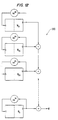
- Circuit 14 includes 67 shift registers, labeled E(0), E(1) ... E(66), each of which is preferably a 10 bit parallel shift register, with the number in parentheses being the power of x represented by that register.
- the data stream of 413 data symbols is read into ECC generator 14 as the data symbols are being sent to disk 26 for storage.
- the mode of generator 14 is then switched by blocking both the data gate 42 and the feedback gate 44 to transfer ECC symbols out of circuit 14 to be appended to the data symbols. Blocking the feedback gate also clears the ECC generator for the next sector's data.
- the ⁇ symbols one of which is labeled 46 in Fig. 2, indicate a parallel .XOR. or modulo-2 add function.
- coefficients of the remaining terms are the normal products of the polynomials, modulo x 10 + x 3 + 1. Because the elements of p and q are binary digits, coefficients of the form pi(qj+qk) are equivalent to pi .AND. (qj .XOR. qk) and may be calculated in hardware in the normal manner. Any product is an .AND. and any addition in parentheses is a modulo-2 addition, of .XOR.
- a 67 symbol "coset leader” is .XOR.'d with the 67 ECC symbols as they are shifted out of circuit 14.
- the coset leader prevents the decoding position of circuit 10 from misinterpreting and accepting a sector that has improperly been shifted.
- a shift of bits that have been .XOR.'d with the coset leader causes circuit 10 to interpret all data in that sector as containing >32 errors.
- the coset leader is .XOR.'d to the ECC symbols in the normal manner.
- the 67 coset leader symbols of the present invention are selected from a code word of a Reed-Solomon code that contains the Reed-Solomon code of the present invention as a subset. As determined by experimentation, the code word from which the coset leader is selected must have no more than 67 non-zero symbols. There is no known method for selecting an optimum coset leader, but the coset leader of the preferred embodiment, shown in Table 1, will result in 33 or more errors if the symbols of the code word are shifted by up to 100 bits. Starting with the last symbol, the coset leader symbols in octal are: TABLE 1 Symbol No.
- FIG. 3 shows the sequence of events performed by the decoder portion of circuit 10 which includes syndrome generating means, step 102; the means for calculating error locator polynomial NU(x), step 104, and error evaluator polymonial W(x), step 106; and means for simultaneously calculating the value of the error locator polynomial NU(x), steps 108, 110, and 112, and the value of the error evaluator polynomial W(x), step 114, and means for correcting erroneous symbols in code word y(x) to error free symbols a i in real time as each root of NU(x) and value of W(x) is calculated, steps 116, 118, 120 and 122.
- N represents the code length in symbols
- I represents the symbol number.
- Syndrome computer 16 of Fig. 1 generates syndromes S i , step 102 of Fig. 3, which are the coefficients of a polynomial S(x).
- Fig. 4 shows the circuit used to compute S(x) simultaneously as the symbols of code word y(x) are read from a sector of disk 26.
- the calculation being performed by the circuit of Fig. 4 is: The calculation is performed by Galois Field multiplier means consisting of an array of 10 bit wide registers, labeled S 33 to S- 33 , GF multipliers, adders, and .AND. gates, each of which is an S computer.
- Galois Field multiplier means consisting of an array of 10 bit wide registers, labeled S 33 to S- 33 , GF multipliers, adders, and .AND. gates, each of which is an S computer.
- x ⁇ i symbols indicate a GF multiply operation
- 0 symbols indicate a modulo-2 addition, or .XOR.
- a mode switch occurs by deasserting feedback gate 150 after 479 symbols have been transferred into all 67 S computers, at which point all 67 .AND. gates, one of which is identified as 152, are blocked and the 480th symbol is simultaneously entered into the 67 S computers. Blocking feedback gate 150 clears all S computers in preparation for calculating syndromes for the next sector.
- a substantial reduction in hardware was achieved by making the Galois Field multiplier means of the syndrome computer of Fig. 4 operate on a half symbol clock (70 ns.) even though it accepts input symbols at half that rate.
- This allows a hardware savings because each multiplier can be used twice in a full symbol period to generate two partial syndromes, therefore only 34 of the 67 alpha multipliers need be built.
- the 67 syndrome values S i are next passed to the S'(K) registers of amend syndrome circuit 200 of Fig. 5. Except for syndrome value S 33 , syndrome values are input through multiplexers, one of which is identified by the numeral 204. This releases the S calculator circuit of Fig. 4 to calculate syndromes for the next code word to be read. Circuit 200 is also part of syndrome generator 16 of Fig. 1.
- the amend syndrome function shortens the code symbols of GF(2 10 ) from a maximum of 1023 symbols to the 480 symbols used in the example and stores the amend syndromes for the shortened code in the SY registers, 210 of Fig. 5.
- Amend syndrome computation starts with a broadside load of the 67 syndromes, S(K), into S'(K) registers, labeled S'(-33) to S'(33).
- register 202 is cleared and loaded with the value of ⁇ 462 , which is equal to 0001010101.
- the first multiplication to take place in GF multiplier 206 is S(-33) x ⁇ 462 which is then shifted into shift register SY(O).
- Multiplexer 208 isolates the ⁇ 462 signal from registers 202 and aligns the GF x ⁇ 544 multiplier so that when syndrome S(-32) is shifted into register S'(-33) it will be multiplied by the contents of register 202 which is the GF product of ⁇ 462 and ⁇ 544 .
- Each amend syndrome in register SY(K) is therefore the GF product of the syndrome value from the S'(K) register multiplied by ( ⁇ 462 )( ⁇ 544 ) n-1 .
- the x ⁇ 544 function is the same GF multiplication defined by Equation 5, but may be implemented by the following .XOR. operations, where O i are the output bits of a 10 bit symbol, and I i are the input bits.
- the ⁇ 462 and ⁇ 544 multipliers of circuit 200 are programmable in the circuit of the preferred embodiment and must be changed if the code word length is altered from 480 symbols.
- Fig. 1 The means for generating the NU(x) error locator polynomial is shown in Fig. 1 as circuit 18. Amend syndromes, SY(K) are now used to compute NU(x) using the Berlekamp-Massey algorithm, as modified by weng, and using a data flow technique as suggested by Riggle to increase processing speed, step 104 of Fig. 3, and shown more completely as the flow chart of Fig. 6.
- FIG. 6 shows the individual steps performed during the calculation of NU(x).
- Fig. 6 is broken down into sections by clock cycles or states, described in more detail hereinbelow, to show operations performed simultaneously. For the sake of clarity, quantities calculated in one section of the chart are made available to other boxes in the chart, but connecting lines are not shown.
- the initial conditions for Fig. 6 are shown in step 252.
- a state machine (not shown) controls the process steps which are repeated 67 times. Referring also to Fig. 7, during state 1, multiplexers (not shown) connect 32 symbol wide GF multiplier 350 to 32 SY registers 210 (SY(1)-SY(32)) and 32 NU registers 352. The GF product is performed as defined by Equation 5 on the NU and SY registers. This completes step 254 of Fig. 6.
- the single 10 bit symbol is clocked into DU registers 358 and is clocked to the output stage of registers 358 during state 2.
- the counting register 360 of Fig. 7 containing counter variable LLMR is decremented by 1 and tested for a condition of being less than 0. If less than 0, gate 362 is enabled.
- the GF inverse circuit 364 of Fig. 7 is shown in more detail in Fig. 9.
- the circuit of Fig. 9 computes the inverse ⁇ -n of an input symbol ⁇ n by raising the input symbol to 32 power and multiplying it by the input symbol lowered to the -33 power.
- the result of ⁇ 32n x ⁇ -33n is ⁇ -n .
- To accomplish this a 10 bit symbol ⁇ n is input to an ⁇ 32 .XOR.
- ⁇ 32n is multiplied by ⁇ n to get ⁇ 33n .
- ⁇ 33n are elements of a subfield, GF(2 5 ), of GF(2 10 ), there are only 31 possible non-zero values for any ⁇ 33n .
- Using a selected 5 of the 10 bits available I 0 , I 1 , I 2 , I 3 , I 5 ), it is possible to construct a logic network as defined by Table 5 below which outputs the 31 inverses of ⁇ 33n (i.e., all ⁇ -33n ).
- O I are the output bits of a ⁇ -33n network that are combusted from the input bits I i .
- the input bits are the 10 bits of the symbol ⁇ 33n and the output bits are the 10 bits of the symbol ⁇ 33n and the output bits are the 10 bits of the symbol ⁇ -33n .
- the final operation to invert ⁇ n is to multiply ⁇ 32n by ⁇ -33n to yield ⁇ -n according to equation 5, presented earlier.
- step 268 of Fig. 6 NR input contents are replaced by NU contents, step 270, and the value of P is replaced by the value of Y. If EN is not set, then NR is shifted upwards (towards higher order terms). Also during state 3, NU input contents are replaced with the NU outputs .XOR.'d with NR ⁇ Q, step 274 of Fig. 6, and SY registers are shifted upwards, step 266. When this has been completed, one of 67 loops has been completed as counted by R in step 276 of Fig. 6. During the 67th loop, the SY register shift is omitted to prepare for the W(x) computation.
- Circuit 448 of Fig. 10 includes means for calculating error evaluator polynomial W(x).
- the means for computing the values of error evaluator polynomial W(x) comprises w registers 450, amend syndrome 54 registers 210, error located polynomial NU registers 352, multiplier 350, and treed adder 354 which executes the procedure shown in Fig. 3, including, specifically step 106.
- the calculation is shown in step 106 in an inverse form.
- the coefficients of W'(x) are the coefficients of W(x) only in reverse order.
- the mode of the NU(x) computer changes to a W(x) computer mode, shown in Fig. 10.
- Multiplexers (not shown) are set to connect NU registers 352 and SY registers 210 to GF multiple 350 and tree'd .XOR. function 354 throughout computation of W(x).
- Ten bit bus 356 is connected to register W(31) of W(I) shift registers 450.
- W(I) registers 450 contain the coefficients of error evaluator polynomial W(x) and the NU(I) registers 352 contain the coefficients of the error locator polynomial NU(x).
- NU(I) and W(I) values are then transferred to the next functions, steps 108, 110, 112, and 114 of Fig. 3.
- Registers 210, 352, and 450 are clearly in preparation for computing NU(x) and W(x) for the next code word.
- the circuits of Fig. 13 provide the means for simultaneously solving the error locator polynomial NU(x), for obtaining the corresponding error value from NU(x) and W(x), and for correcting erroneous symbols in code word y(x) to error free symbols a i as each symbol is shifted out of buffer 22 of Fig. 1, which includes the steps of (1) solving each term of NU(x), summing the odd and even power terms into NU odd (x) and NU even (x) respectively, step 108 of Fig. 3, (2) simultaneously evaluating W(x), and (3) correcting errors in y(x) as indicated by the error locations and error values derived from the calculated values of NU odd (x) and W(x).
- the error value computation circuit 20 of Fig. 1 evaluates the 32 symbol values of NU(x) plus the lowest order coefficient of NU(x) which is always 1, and the 32 symbol values of W(x) for each code word symbol within the sector in real time at the same time as the corresponding symbol is shifted out of buffer 22 of Fig. 1. The results of these evaluations are then manipulated to generate the actual correction polynomial p(x).
- the usual practice is to use a Chien search, where all possible legitimate values of x are tested to find the roots of NU(x). Based on those roots, the erroneous symbols are identified, W(x) evaluated, and y(x) later corrected.
- the standard technique requires more latency than the present invention.
- the Chien search is modified to permit simultaneous evaluation of W(x), data flow is pipelined, and erroneous symbols are identified and corrected in real time as they exit buffer 22 of Fig. 1 on their way to data processing bus 28.
- Circuit 480 of Fig. 11 consisting of a plurality of Galois Field multiplier means, each containing a 10 bit shift register and a Galois Field multiplier network, evaluates NU ( ⁇ i ) as each code symbol is timed to exit buffer 22 of Fig. 1, where i is the number of the symbol exiting buffer 22 of Fig. 1.
- the contents of each NU register NU 1 to NU 32 is multiplied by the GF multiplier connected to the register, thereby testing for a root ⁇ i of NU for each clock cycle.
- the contents of each NU register of circuit 480 is multiplied by its corresponding GF multiplier once for each corresponding data symbol.
- NU even and NU odd are summed separately and are referred to as NU even and NU odd .
- NU odd is required for subsequent error value calculations.
- W(x) is also being evaluated by circuit 500 of Fig. 12 once for each symbol exiting buffer 22.
- circuit 500 of Fig. 12 computes W ( ⁇ i ) x ⁇ 34i for each symbol, corresponding to step 116 of Fig. 3.
- circuit 480 is the same circuit as shown in Fig. 11, and circuit 500 is the same circuit as shown in Fig. 12.
- divider circuit 524 computes the correct value, or correction vector of the i th code word symbol. This is shown as YI in step 116 of Fig. 3 and will be discussed in more detail hereinbelow.
- Divider circuit 524 of Fig. 13, shown in greater detail in Fig. 14, operates in a similar manner to the GF inverse circuit of Fig. 9 except that a second input and third multiplier have been added.
- Divider 524 calculates the correction vector YI, step 116 of Fig. 3, by dividing Z from step 114, which is represented by symbol ⁇ m of Fig. 14, by NU odd , which is represented by symbol ⁇ n of Fig. 14.
- the resulting correction vector is therefore: Equation 8
- ⁇ YI W( ⁇ i)( ⁇ 34i )/NU odd This completes step 116 of Fig. 3.
- Circuit 24 of Fig. 1 amends erroneous code word symbols by .XOR.ing the data stream from buffer 22 with the correction vectors, step 122 of Fig. 3.
- gate 530 of Fig. 13 is open and the correction vector is zero, therefore .XOR. circuit 24 leaves the data symbol unchanged.
- the buffer data stream must be synchronized with the computation of error values so that the correction vectors match the correct data symbols.
- Buffer circuit 22 of Fig. 1 is a large first-in-first-out storage unit for data read from disk data port 26 and provides data to amend circuit 24 approximately 2 sector times following data entry to the buffer.
- the input symbols are latched into a shift register once for each symbol read time, generating a 30 bit word.
- Each group of 3 symbols shifted in is written to a holding register, then later transferred into the buffer where the group remains until the end of the two sector delay time, whereupon the group of 3 symbols is received by a read shift register and sent to the data amend function 24 of Fig. 1, one symbol at a time.
- the final function performed by the decoding circuitry is conversion of the amended 10 bit symbols into 16 bit data words and EDC words by converter 27 of Fig. 1.
- Bits 0-9 of the first data word are bits 0-9 of the first symbol.
- Bits 10-15 of the second data word are bits 0-5 of the second symbol. Conversion continues for all data words so that bits 0-7 of symbol 413 are bits 8-15 of the last data word, and bits 8 and 9 of the 413th symbol are discarded.
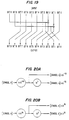
- Fig. 15 shows the time allocations for major data shifts and computations performed by the encoding and decoding circuits.
- the data flow between sections of circuit 10 is unidirectional, that is, there is no handshaking. Each section is ready to accept new data when the previous section is ready to supply it.
- the chip manipulates data in a synchronous manner, having one single clock source.
- the cycle time of the clock in the preferred embodiment is nominally 70 ns which is half-symbol time.
- a full symbol time in the preferred embodiment is 140 ns.
- Decoding commences with data symbols being read from the data storage device 26 into buffer 22 and syndrome computer 16 of Fig. 1, time slots 600 and 602 of Fig. 15, respectively. ECC symbols at time slot 604 are also read into syndrome computer 16. Buffer 22 holds data read during time slot 600 for approximately two sector times and does not release the data until time slot 606. As data in time slot 602 are being read into syndrome computer 16 of Fig. 1, the syndrome computer begins processing data during time slot 608. Following syndrome and amend syndrome computation, error evaluator polynomial W and error locator polynomial NU are computed during time slots 610 and 612 and are used to calculate correction vectors YI at time slow 614 as data symbols are being released from buffer 22 in time slow 606.
- syndrome computer 16 is now ready to begin computations on the next code word at time slot 616, with syndromes for these data being computed during time slot 618, and error evaluator and error locator polynomials being computed during time slots 620 and 622 respectively.
- Correction vectors during time slot 624 are calculated for the data of time slot 616 as they are released from buffer 22 during time slot 626.
- a savings is made in hardware in the exclusive OR (.XOR.) networks used to implement the GF x ⁇ i multiplications shown in Fig. 4 for the syndrome computer, Fig. 12 or Fig. 13 for the error evaluator polynomial W(x) computer, and Fig. 11 or Fig. 13 for the NU odd and NU even computers.
- .XOR. exclusive OR
- the ⁇ symbols are .XOR. gates.
- the input is a 10 bit symbol [SYMBOL A] and the output is a 10 bit symbol [SYMBOL A] x ⁇ -33 .
- the size of this kind of .XOR. network is large, requiring 59 .XOR. gates for the ⁇ -33 multiplier of Fig. 16, and 60 .XOR. gates for the ⁇ -32 multiplier of Fig. 17.
- These large .XOR. networks are complex to implement at the VLSI level, therefore, it is difficult to build many of them in a small silicon integrated circuit.
- the second preferred embodiment of the present invention provides an improved Galois Field multiplier means which reduces the number and complexity of these GF multiplier circuits.
- ⁇ i x ⁇ j ⁇ i+j .
- ⁇ -32 may be generated by multiplying ⁇ -33 by ⁇ 1 .
- a given a multiplier may therefore be constructed from products of simpler multipliers.
- the circuit of Fig. 18 shows an ⁇ 1 multiplier circuit, or Shift-1 circuit, which uses one .XOR. gate to perform a modulo-2 addition (bit 9 .XOR. bit 2) to generate the output bit 3 and also uses some cross-connected input and output lines to transpose bits to provide the desired output.
- the circuit of Fig. 19 shows an ⁇ 2 multiplier circuit, or Shift-2 circuit, consisting of two .XOR. gates and cross-connected inputs and outputs to produce the desired output.
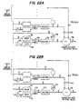
- Fig. 20a and 20b show how the product of a complex ⁇ multiplier, ⁇ -33 or ⁇ 30 , and a simple multiplier, ⁇ 1 or ⁇ 2 can produce an output that ordinarily would require two complex multipliers, thereby considerably reducing circuit complexity.
- an ⁇ -33 and an ⁇ 1 multiplier produce an output consisting of the input symbol [SYMBOL A] times ⁇ -33 and also times ⁇ -32 for a net savings of 59 .XOR. gates, or one ⁇ -32 multiplier network.
- the values of [SYMBOL B]X ⁇ 30 and [SYMBOL B] x ⁇ 32 are generated using a ⁇ 30 multiplier and a Shift-2 circuit, thereby eliminating an ⁇ 32 multiplier.
- Fig. 21 shows the syndrome computer of Fig. 4 configured according to the second preferred embodiment to exploit the technique of reducing the complexity of the GF multipliers.
- S(-30) to S(-33) registers and related GF multiplier and multipliers (MUXes) are shown and described; the rest being repetitive.
- MUXes GF multiplier and multipliers
- Syndrome computer 16 of Fig. 1 processes one symbol through the syndrome compute circuit of fig. 4 or Fig. 21 approximately every 140 ns (a full symbol clock) in both preferred embodiments.
- the syndrome compute circuit consists of a plurality of Galois Field multiplier means each comprising two 10-bit registers coupled to modulo-2 adder by a 2-to-1 multiplexer, a hold register, a complex GF multiplier .XOR. network, and a simple Shift-1 multiplexer.
- all S registers, 702, 704, 706, and 708 of Fig. 21, are cleared by a signal on reset line 738.
- the 2-to-1 multiplexers (2-to-1 MuXes) 710 and 712 are enabled to allow the contents in the odd numbered S registers, S(-33), S(-31), etc. to modulo-2 add their contents by GF addition in adders 714 and 716 to the 10 bit data symbols from disk 26 of Fig. 1.
- the resulting sums are stored in hold registers 718 and 720.
- the contents of the hold registers are next multiplied by the GF multipliers, ⁇ -31 and ⁇ -33 , 722 and 724, and the resulting product is loaded into S(-31) and S(-33) registers 704 and 708.
- the contents of S(-31) register 704 are [(previous S(-31) register contents) + (data symbol from disk 26)] x ⁇ -31
- the contents of S(-33) register 708 are: [(previous S(-33) register contents) + (data symbol from disk 26)] x ⁇ -33 .
- the 2-to-1 MUXes 710 and 712 are enabled to select the contents in the even numbered S registers 702 and 706, only two of which are shown in Fig. 21, and add the contents of the even numbered S registers to the same ten-bit symbol present on the data-in bus from disk 26 in adders 714 and 716.
- the result is stored in hold registers 718 and 720.
- the contents in the hold registers 718 and 720 are again multiplied by the GF multipliers, ⁇ -31 and ⁇ -33 , 722 and 724 respectively of Fig.
- the output values are next multiplied by the Shift-1 circuits 726 and 728, and the results are stored in registers 702 and 706.
- the contents of S(-30) register 702 are [(previous S(-30) register contents + (data symbol from disk 26)] x ⁇ -30 and the contents of S(-32) register 706 are [(previous S(-32) register contents) + (data symbol from disk)] x ⁇ -32 . This add and multiply calculation is repeated for the next ten-bit data symbol retrieved from the disk.
- an output value of S is provided from the output of each adder associated with each S register as shown in Fig. 4.
- one output line for example 730 of Fig. 21, provides the output for two S registers, 706, 708.
- One value of S is output every half symbol clock to multiplexer 732 which directs the symbol to its respective S' register of Fig. 5 via lines 734 and 736.
- Figs. 22a and 22b show the error locator polynomial NU(x) computer circuit 480 of Fig. 11 or Fig. 13 for computing NU odd and NU even configured to according to the second preferred embodiment to exploit the technique of reducing the complexity of the GF multipliers.
- Figs. 22a and 22b show only small portions of the computers to illustrate the implementation of the technique.
- the circuits of Figs. 22a and 22b perform the same functions as the equivalent circuits 480 of Fig. 11 or Fig. 13 in the first preferred embodiment, therefore the function of these circuits will not be discussed further. Only the application of the GF multiplier hardware reduction techniques to the error locator computer will not be discussed.
- the NU even and NU odd computer consists of a plurality of Galois Field multiplier means, each comprising two 10-bit shift registers coupled to a hold register by a 2-to-1 multiplexer, a complex GF multiplier .XOR. network, and a simple Shift-2 multiplier for repetitively multiplying the contents of the shift registers by a value of ⁇ i .
- a set of ten-bit symbol values are loaded into all NU even numbered registers 750, 752 (only a representative two of which are labeled) and all NU odd numbered registers 771, 773 (only a representative two of which are labeled) from bus 456 connection now shown).
- the 2-to-1 MUXes 754, 775 are enabled to copy the contents of the NU(30) and NU(29) registers, 750, 771 respectively, into the hold registers 756, 777.
- the contents of hold registers 756, 777 are then multiplied by ⁇ 30 and ⁇ 29 GF multipliers 758, 779.
- the outputs of GF multipliers 758, 779 are loaded back into the corresponding NU(30) and NU(29) registers, 750, 771.
- the contents of NU(30) register 750 is now equal to [previous NU(30) register contents] ⁇ 30 and the contents of NU(29) register 771 is [previous NU(29) register contents]X ⁇ 29 .
- the 2-to-1 MUXes 754, 775 are enabled to copy the contents in the NU(32) and NU(31) registers 752, 773 into their respective hold registers 756, 777.
- the contents of the hold registers are next multiplied by the same GF ⁇ 30 and ⁇ 29 multipliers, 758, 779.
- the output values of the GF multipliers 758, 779 are loaded back into the corresponding NU(32) and NU(31) registers 752, 773 after being multiplied by ⁇ 2 in the respective Shift-2 circuits 762, 783.
- the contents of NU(32) register 752 is equal to [previous NU(32) register contents] x ⁇ 31 . This process is again repeated in the next symbol clock.
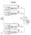
- Fig. 23 shows the error evaluator polynomial W(x) computer circuit 500 of Fig. 12 or Fig. 13, configured to according to the second preferred embodiment to exploit the technique of reducing the complexity of the GF multipliers.
- Fig. 23 shows only a small portion of the computer to illustrate the implementation of the technique.
- the circuit of Fig. 23 performs the same functions as the equivalent circuit 500 of Fig. 12 or Fig. 13 in the first preferred embodiment, therefore, the function of this circuit will not be discussed further. Only the application of the GF multiplier hardware reduction techniques to the error evaluator computer will now be discussed.
- Error evaluator circuit 800 consists of a plurality of Galois Field multiplier means, of the same form as the NU odd and NU even circuits of Figs. 22a and 22b, for repetitively multiplying the contents of the NU registers by ⁇ i , and functions in a similar manner. Even values of W() are calculated and stored in the even W registers during one half symbol clock and odd values are calculated and stored in the odd W registers during the next half symbol clock. Only even numbered ⁇ multipliers are provided; the odd ⁇ multipliers are provided by the shift-1 circuit.
- accumulator 804 stores and adds the even and odd outputs of adder 802 to provide the full value of W() for computation of the correction vector as shown on Fig. 13.
Abstract
Description
- This invention relates to using VLSI architecture for high bandwidth, low latency execution of the Reed-Solomon encode, decode, and error correction functions, capable of correcting a large number of symbol errors in binary digital data.
- Electronic communications and data processing systems transmit, receive and store electromagnetic signals representative of binary "zeros" and "ones." During data transfer along data channels, or during the process of storing data on and retrieving data from various magnetic, optical or other storage media, erroneous data values may occur. These errors may be the result of electromagnetic noise on the data channel or defects in the storage media. Isolated single bit random errors and contiguous multibit "bursts" of errors must be recognized and corrected using a system that is highly reliable, that is, one that does not produce many errors in the corrected data. At a minimum, the erroneous data must be recognized and flagged as erroneous rather than being acted upon.
- Unlike data communications systems that have the luxury of retransmitting data until anerror free transmission occurs, erroneous data stored on magnetic, optical or other storage media are permanently lost unless they can be corrected. By encoding data prior to storage or transmission, and decoding following reception or retrieval, errors may be detected and corrected prior to the data being released for subsequent use. Reed-Solomon codes are effective for the types of independent and bursty errors experienced on magnetic storage media. Information on encoding, decoding, and Reed-Solomon codes in particular may be found in "Error Correcting Codes" by Peterson and Weldon, The MIT Press, second edition (1972) and several other texts.
- For binary data storage and retrieval systems, error correction begins prior to storing data on the applicable medium, here considered to be a magnetic disk. First the data are encoded using an (N,K) Reed-Solomon code word of N m-bit symbols, consisting of K data symbols and N-K Error Correction Code (ECC) symbols. The ECC symbols are redundant and provide the information necessary to recognize erroneous data symbols and to reconstruct a maximum of T = (N-K)/2 data symbols.
- A symbol is a series of m bits, for example, 6 or 10. The data stream of binary digits destined for storage on a disk sector usually consists of a series of 8, 16 or 32 bit words and must be converted to a series of data symbols. The N symbols of the code word are representative of the coefficients of a polynomial in x of degree N-1 represented by a(x) where deg(a)=N-1. ECC symbols are generated such that each code word is evenly divisible by a generator polynomial, g(x), having N-K consecutive roots in the Galois Field, GF (2m), and where each ECC symbol is an element αi of GF(2m). The generator polynomial, g(x) is chosen based on the extent and complexity of the error correction scheme, that is, how many symbols of detection and correction are desired. In an (N,K) code, deg(g)=N-K. If d(x) is a polynomial in x of degree K-1 with K data symbols di as coefficients, then the code word a(x) is:


- The factors of an error locator polynomial, NU(x), an error evaluator polynomial, W(x), locate the erroneous data symbols within the code word and indicate the values which, when added
modulo 2 to the received symbols, provide the correct symbols. The terms of NU(x) are calculated using the Berlekamp Massey algorithm from the error syndromes, Si, which are obtained by dividing y(x) by the factors of g(x). If a syndrome is non-zero, then part of the code word is in error. The error located is found by computing the roots of the error locator polynomial, NU(x) and then the correct data symbol may be determined by finding the value of W(x) using the syndromes and NU(x). Root finding in a digital environment typically uses Chien's search algorithm. A Reed-Solomon encoding-decoding system that uses the technique of a generator polynomial, syndrome computation, and evaluation of error locator and error evaluator polynomials is described in U.S. Patent No. 4,413,339 to Riggle et al. - Because of the many computations being performed in software or iteratively in hardware, and the need to calcuate the NU(x) and W(x) polynomials and all the roots of NU(x), and to evaluate W(x) prior to correcting erroneous data symbols, prior art decoders suffer from one or more of the drawbacks of high latency, low bandwidth and high cost, especially when many data errors are encountered. Soft error rates for disks are therefore limited to about 1 x 10⁻⁶ because of the low processing speed or cost of the decoders. Faster Reed-Solomon systems which are also inexpensive have the drawback of being limited to correcting a maximum of only about 4 symbols per sector, which limits the tolerable soft error rates for data storage devices. Cross-interleaved Reed-Solomon decoders have a moderate bandwidth and can correct large numbers of symbol errors, but they introduce excessive storage overhead for disk systems with short disk blocks, thereby reducing the net data density permitted on the disk drive. This defeats one of the primary purposes for implementing the ECC system, which is to allow high density data storage on disk drives along with the inherently high data error rates resulting from increased density data storage.
- EP-0114938 describes an error detection and correction system according to the preamble of
claim 1. - An object of this invention is to correct higher soft bit error rates on sectorized data storage devices while providing acceptably low hard bit error rates.
- Another object of this invention is to provide a high bandwidth, low latency implementation of the Reed-Solomon error correction function where a large number of symbol errors are corrected with a minimum of data storage overhead within a standard disk block.
- A further object of this invention is to implement pipelining and flow control processes for executing the Berlekamp-Massey, Weng and modified Chien algorithms, and to provide novel algorithms for computing the degree of the error location polynomial and its control over the Berlekamp-Massey algorithm, so that the Reed-Solomon error correction function can be implemented in hardware in real time.
- Additional objects and advantages of the invention will be set forth in the description which follows, and in part will be obvious from the description, or may be learned by practice of the invention. The objects and advantages of the invention may be realized and obtained by means of the instrumentalities and combinations particularly pointed out in the appended claims.
- U.S. Patent Application No. 050,725, corresponding to EP-0318547, titled "Real-Time BCH Error Correction Code Decoding Mechanism" by Lih-Jyh Weng filed on May 15, 1987, and assigned to the same assignee as the present invention.
- U.S. Patent Application No. 067,712, corresponding to EP-0328637, titled "Apparatus for Computing Multiplicative Inverses in Data Encoding and Decoding Devices" by Lih-Jyh Weng filed on June 26, 1987, and assigned to the same assignee as the present invention.
- The present invention is set out in
claims 1 and 13. - The accompanying drawings, which are incorporated in and constitute a part of the specification, illustrate a preferred embodiment of the invention and, together with the general description given above and the detailed description of the preferred embodiment given below, serve to explain the principles of the invention.
-
- Fig. 1 is a schematic block diagram showing the overall structure of an integrated circuit which constitutes a preferred embodiment of the present invention;
- Fig. 2 is an electrical schematic diagram showing the major steps performed by the ECC Generator of the circuit of Fig. 1;
- Fig. 3 is a flow chart of the decoding process performed by the syndrome computer, the error locator NU(X) and error evaluator W(x) computer, and the factor NU(x), evaluate W(x), and correction vector YI computer circuits of Fig. 1;
- Fig. 4 is an electrical schematic diagram of the Syndrome Compute circuit, part of the
Syndrome Computer block 16 of the circuit of Fig. 1 and part ofstep 102 of the flowchart of Fig. 3; - Fig. 5 is an electrical schematic diagram of part of the Amend Syndrome Compute circuit, another part of the
Syndrome Compute block 16 of the circuit of Fig. 1 and apart ofstep 102 of the flowchart of Fig. 3; - Fig. 6 is a flowchart of the computation of the error locator polynomial NU(x),
step 104 of Fig. 3 and part of the Compute Error Locator NU(x), Error Evaluator W(x)circuit 18 of Fig. 1; - Fig. 7 is an electrical schematic diagram of the execution of Berlekamp's algorithm as shown in the flowchart of Fig. 6;
- Fig. 8 is an electrical schematic diagram of the remaining part of the execution of Berlekamp's algorithm as shown in the flowchart of Fig. 6;
- Fig. 9 is an electrical schematic diagram of a Galois Field combinational inverse calculator, which is
circuit 364 of Fig. 7; - Fig. 10 is an electrical schematic diagram of the circuit that computes the error evaluator polynomial W(x), namely
step 106 of Fig. 3; - Fig. 11 is an electrical schematic diagram of the circuit that computes the value of the error locator polynomial NU(x) in real time for each symbol of the code word, namely
steps - Fig. 12 is an electrical schematic diagram of the circuit that computes the value of the error evaluator polynomial W(x) in real time for each symbol of the code word, namely
step 114 of Fig. 3; - Fig. 13 is an electrical schematic diagram of the circuit that computes the error locations and correction vectors of code word symbols in real time, comprising the circuits of Figs. 11 and 12, and also including
steps - Fig. 14 is an electrical schematic diagram of the Galois Field divide calculator, which is
circuit 524 of Fig. 13; - Fig. 15 is a timing diagram showing the time allocations for calculations and data transfers in the circuit of the present invention;
- Fig. 16 is an electrical schematic diagram of an .XOR. network that functions as a GF α-33 multiplier;
- Fig. 17 is an electrical schematic diagram of an .XOR. network that functions as a GF α-32 multiplier.
- Fig. 18 is an electrical schematic diagram of an .XOR. network known as a Shift-1 circuit that performs the function of a GF α1 multiplier;
- Fig. 19 is an electrical schematic diagram of an .XOR. network known as a Shift-2 circuit that performs the function of a GF α2 multiplier;
- Fig. 20A is an electrical schematic diagram of a circuit to compute [SYMBOL A] x α-33 and [SYMBOL A] x α-32 using the α-33 multiplier of Fig. 16 and the α1 multiplier of Fig. 18;
- Fig. 20B is an electrical schematic diagram of a circuit to compute [SYMBOL B] X α30 AND [SYMBOL B] x α32 using an α30 multiplier and the Shift-2 circuit of Fig. 19;
- Fig. 21 is an electrical schematic diagram of a preferred embodiment of the Syndrome Compute circuit of Fig. 4 using the Shift-1 circuit of Fig. 18 to eliminate approximately half of the multiplier circuitry;
- Fig. 22A is a second preferred embodiment of the NUeven circuit Fig. 13 using the Shift-2 circuit of Fig. 19;
- Fig. 22B is an electrical schematic diagram of a second preferred embodiment of the NUodd circuit of Fig. 13 using the Shift-2 circuit of Fig. 19;
- Fig. 23 is an electrical schematic diagram of a second preferred embodiment of the error evaluator polynomial W(x) computer of Fig. 12 using the Shift-1 circuit of Fig. 18;
- Reference will now be made in detail to the present preferred embodiment of the invention as illustrated in the accompanying drawings.
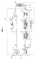
- The present preferred embodiment of the Reed-Solomon error detecting and correcting circuit is shown in block diagram form in Figure 1 and is represented generally by the numeral 10. As embodied herein,
circuit 10 accepts binary data fromdata bus 28 of a data processing system (not shown) and converts those data bits into K m-bit data symbols, di, where i = 1 to K. Data symbols di are simultaneously sent to an Error Correction Code (ECC)generator 14 and adata storage disk 26 through amultiplexer 15. - In accordance with the invention, there is provided encoder means for encoding the data symbols into a plurality of Reed-Solomon first code words a(x) and sending the first code words to the error inducing medium. As embodied herein,
ECC generator 14 generates N-K ECC symbols ei, where =0 to N-K-1, using a generator polynomial g(x) having roots α1, -34 < i < 34, where α is a primitive element of the Galois Field GF(2m). N represents the length of the code word and is an integer < 2m. The N-K ECC symbols ei are appended bymultiplexer 15 to the K data symbols di to create an N symbol Reed-Solomon (N,K) code word a(x), consisting of N symbols ai, which is stored ondata storage disk 26. A header field is also provided for each code word which provides separation between code words, and other storage functions, and is not described in detail.Storage device 26 is an example which contains an error inducing medium where errors can be created as data as being stored and retrieved. - Errors may occur to the symbols of code word a(x) when stored on and retrieved from
storage device 26. When read from the disk, code word a(x) is designated y(x) because it may contain erroneous symbols. Where there are no errors present, y(x) equals a(x), or equivalently p(x) = 0. - In accordance with the invention, there is provided buffer means for receiving from the error inducing medium a plurality of retrieved code words y(x) equal to the first code words in which errors have been induced and for holding each of the retrieved code words long enough to compute error locations and values, preferably for no longer than the time needed to compute error locations and values. As embodied herein, data symbols read from
data storage disk 26 are held in adata buffer 22. The invention further includes decoder means for computing from the retrieved code words a plurality of error locations and correction vectors in real time as each symbol of the retrieved code word exits from the buffer means. As herein embodied, the decoding means, including aSyndrome Computer 16, an Error Locator and anError Evaluator Computer 18, and an ErrorCorrection Vector Computer 20, calculates the error location and correction vector for data symbols being held inbuffer 22. - As herein embodied,
Syndrome Computer 16 begins calculating syndromes as the code word symbols are read fordata storage device 26. Error locator anderror evaluator computer 18 computes the error locator polynomial NU(x) by solving the Berlekamp-Massey algorithm using syndromes computed inSyndrome Computer 16. The terms of error evaluator polynomial W(x) are also calculated incomputer 18 using the values of NU(x) and syndromes fromSyndrome Computer 16. - In accordance with the invention, there is provided correcting means responsive to the error locations and correction vectors for correcting erroneous data symbols as they exit the buffer means. As herein embodied, as each data symbol d'i is released from
buffer 22,computer 20 calculates error locator polynomial NU(x) using a modified Chien search alogorithm, and evaluates error evaluator polynomial W(x) to compute a correction vector YI that is exclusive or'd by .XOR.circuit 24 with the data symbol being released frombuffer 22. Data symbols of the decoded code word are converted into 16 bit data words byconverter 27 and are returned to thedata processing device 16bit data bus 28. - The "pipe-lining" or high speed computation of error values and locations in real time as data are released from
buffer 22 is a major factor in achieving the low latency, or low holdup time, which permits the circuit of the present invention to achieve a high bandwidth. - Using VLSI logic to execute a Reed-Solomon error correcting function, the circuit of the preferred embodiment achieves an acceptably low error rate for decoded data for sectorized data storage devices such as magnetic disks, magnetic tapes, and optical disks having high inherent error rates. The circuit provides a high bandwidth of approximately 70 megabits per second and a low latency of about 144 microseconds at peak bandwidth using a standard disk sector size of 480 symbols where up to 32 ten bit symbols may need to be corrected, requiring an overhead of 670 ECC bits.
- Preferably, and as shown in Fig. 1, binary data bits destined for storage on
magnetic disk 26 are received from a data processing system (not shown) via a 16bit data bus 28. The binary data, which consist of both information words and Error Detecting Code (EDC) words are converted inconverter 12 to a series of K symbols, where each symbol is m-bits long. In the preferred embodiment, each symbol is 10 bits long, and K is selectable from 48 to 941 data symbols. The 10 bit symbols are assembled from data words and EDC words, each word being 16 bits long. The 16 bit words are converted to symbols until all data words and EDC words have been converted to ten bit data symbols, represented by di. Enough fill bits are added to provide complete symbols. Data symbols di are sent both tostorage disk 26 andECC generator 14. - As here embodied, the encoder means includes
ECC generator 14. ECC symbols ei which will be used to detect and correct errors in the data symbols di are computed byECC generator 14 using a generator polynomial g(x). The error correction code chosen is a symmetric Reed-Solomon code over the Galois Field GF (210) generated by the primitive polynomial x10 + x3+ + 1. For the Reed-Solomon code of the preferred embodiment, the generator polynomial, g(x) is defined as:
integrated circuit 10 of Fig. 1. The generator polynomial g(x) is chosen to generate 67 ECC symbols, therefore N-K is 67 which suffices to correct up to 32 symbols in error per sector or code word, provide a 100% probability of detecting all errors up to 35 errors per sector, and provide a strong likelihood of detecting all errors greater than 35 per sector. The polynomial g(x) is so defined that when expanded into its individual terms, it has symmetric coefficients so that the Galois Field multiplier circuits, defined mathematically below, can be reduced by a factor of 2, that is, each αi term appears twice in g(x) as a coefficient of a different power of x.Equations Equation 1.Equation 3 shows the individual terms of g(x).

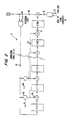
- Fig. 2 shows the circuit used by
ECC generator 14 to generate the 67 ECC symbols ei by dividing, d(x) ∗ xN-K by g(x), where d(x) is a polynomial of degree K-1 with coefficients equal to di. Mathematically, the code word a(x) is a polynomial with coefficients ai and consists of the 67 ECC symbols ei appended to the data symbols, di. Note that in the examples which follow, exactly 413 data symbols are chosen. Syndrome modifiers referenced later are based on this choice of 413 data symbols. If a(x) is considered to be an N-1 degree polynomial in x with the symbols ai as coefficients, then
Circuit 14 includes 67 shift registers, labeled E(0), E(1) ... E(66), each of which is preferably a 10 bit parallel shift register, with the number in parentheses being the power of x represented by that register. The data stream of 413 data symbols is read intoECC generator 14 as the data symbols are being sent todisk 26 for storage. The mode ofgenerator 14 is then switched by blocking both thedata gate 42 and thefeedback gate 44 to transfer ECC symbols out ofcircuit 14 to be appended to the data symbols. Blocking the feedback gate also clears the ECC generator for the next sector's data. The ⊕ symbols, one of which is labeled 46 in Fig. 2, indicate a parallel .XOR. or modulo-2 add function. The x αi symbols, one of which is labeled 48, indicate a Galois Field multiply by αi, which is equivalent to raising the exponent of an input symbol by i, for example αj ∗ αi = αi+j, where i+j is computed modulo 1023. All GF multiply operations are modulo the primitive polynomial x10 + x3 + 1. - Multiplication on the Galois Field is defined as follows. If p and q are any two 10 bit symbols where each bit is p0, p1, ... p9 and q0, q1, ... q9, then the GF multiply function is defined as:

- Because the Reed-Solomon code is cyclic, a 67 symbol "coset leader" is .XOR.'d with the 67 ECC symbols as they are shifted out of
circuit 14. The coset leader prevents the decoding position ofcircuit 10 from misinterpreting and accepting a sector that has improperly been shifted. A shift of bits that have been .XOR.'d with the coset leader causescircuit 10 to interpret all data in that sector as containing >32 errors. During the data read operation, discussed hereinbelow, the 67 ECC symbols as read from the disk sector are again .XOR.'d with the same coset leader symbols, removing them from the ECC symbols and having no effect on further calculations unless the symbols were shifted, and then excessive errors will be generated in accordance with the normal functioning of the decoding circuit. - The coset leader is .XOR.'d to the ECC symbols in the normal manner. The 67 coset leader symbols of the present invention are selected from a code word of a Reed-Solomon code that contains the Reed-Solomon code of the present invention as a subset. As determined by experimentation, the code word from which the coset leader is selected must have no more than 67 non-zero symbols. There is no known method for selecting an optimum coset leader, but the coset leader of the preferred embodiment, shown in Table 1, will result in 33 or more errors if the symbols of the code word are shifted by up to 100 bits. Starting with the last symbol, the coset leader symbols in octal are:
TABLE 1 Symbol No. Value Symbol Value Symbol Value 0 404 23 324 46 1125 1 1245 24 1722 47 1401 2 1026 25 1413 48 402 3 722 26 1002 49 1564 4 1347 27 777 50 1604 5 1147 28 1370 51 627 6 245 29 1526 52 776 7 1140 30 471 53 1275 8 457 31 1626 54 135 9 560 32 573 55 501 10 164 33 402 56 42 11 1407 34 1562 57 410 12 1647 35 743 58 1632 13 362 36 421 59 1313 14 326 37 1230 60 1223 15 401 38 55 61 531 16 567 39 1453 62 1745 17 314 40 233 63 1442 18 1532 41 257 64 777 19 1142 42 665 65 1632 20 707 43 1525 66 630 21 424 44 1415 22 665 45 1301 - After a varying amount of data storage time determined by the disk user, code word y(x) is read from
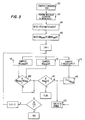
disk 26. Because of possible errors in code word symbols, a(x) is now represented by y(x). If there are no errors in y(x), then a(x) = y(x). The flow chart of Fig. 3 shows the sequence of events performed by the decoder portion ofcircuit 10 which includes syndrome generating means, step 102; the means for calculating error locator polynomial NU(x),step 104, and error evaluator polymonial W(x),step 106; and means for simultaneously calculating the value of the error locator polynomial NU(x), steps 108, 110, and 112, and the value of the error evaluator polynomial W(x),step 114, and means for correcting erroneous symbols in code word y(x) to error free symbols ai in real time as each root of NU(x) and value of W(x) is calculated, steps 116, 118, 120 and 122. On Fig. 3, N represents the code length in symbols and I represents the symbol number. -
Syndrome computer 16 of Fig. 1 generates syndromes Si, step 102 of Fig. 3, which are the coefficients of a polynomial S(x). Fig. 4 shows the circuit used to compute S(x) simultaneously as the symbols of code word y(x) are read from a sector ofdisk 26. The calculation being performed by the circuit of Fig. 4 is:
feedback gate 150 after 479 symbols have been transferred into all 67 S computers, at which point all 67 .AND. gates, one of which is identified as 152, are blocked and the 480th symbol is simultaneously entered into the 67 S computers. Blockingfeedback gate 150 clears all S computers in preparation for calculating syndromes for the next sector. - In a second preferred embodiment a substantial reduction in hardware was achieved by making the Galois Field multiplier means of the syndrome computer of Fig. 4 operate on a half symbol clock (70 ns.) even though it accepts input symbols at half that rate. This allows a hardware savings because each multiplier can be used twice in a full symbol period to generate two partial syndromes, therefore only 34 of the 67 alpha multipliers need be built. Each adjacent multiplier is related by a simple function. As an example, α-32 can be derived by taking α-33 and multiplying it by α1 (-33 + 1 = -32). Multiplying by α1 is equivalent to shifting once and
XORing bit 9 withbit 2. - Given a 10
bit symbol 9 8 7 6 5 4 3 2 1 0, this symbol multiplied by α1 would become 8 7 6 5 4 3 9.XOR.2 1 0 9. This is a much simpler and smaller function to build than an α-32 multiplier. All even numbered alpha multipliers in the syndrome computer are derived from the odd numbered alpha multipliers in this manner. This same hardware reduction technique is also used in theYI computer 20 of Fig. 1, and will be discussed in greater detail hereinbelow. - The 67 syndrome values Si are next passed to the S'(K) registers of amend
syndrome circuit 200 of Fig. 5. Except for syndrome value S33, syndrome values are input through multiplexers, one of which is identified by the numeral 204. This releases the S calculator circuit of Fig. 4 to calculate syndromes for the next code word to be read.Circuit 200 is also part ofsyndrome generator 16 of Fig. 1. The amend syndrome function shortens the code symbols of GF(210) from a maximum of 1023 symbols to the 480 symbols used in the example and stores the amend syndromes for the shortened code in the SY registers, 210 of Fig. 5. Amend syndrome computation starts with a broadside load of the 67 syndromes, S(K), into S'(K) registers, labeled S'(-33) to S'(33). Simultaneously, register 202 is cleared and loaded with the value of α462, which is equal to 0001010101. Multiplexers connected to S'(K) registers to the next higher S'(K-1) register. The first multiplication to take place inGF multiplier 206 is S(-33) x α462 which is then shifted into shift register SY(O).Multiplexer 208 isolates the α462 signal fromregisters 202 and aligns the GF x α544 multiplier so that when syndrome S(-32) is shifted into register S'(-33) it will be multiplied by the contents ofregister 202 which is the GF product of α462 and α544. Each amend syndrome in register SY(K) is therefore the GF product of the syndrome value from the S'(K) register multiplied by (α462)(α544)n-1. The x α544 function is the same GF multiplication defined byEquation 5, but may be implemented by the following .XOR. operations, where Oi are the output bits of a 10 bit symbol, and Ii are the input bits.Table 2 O9 = I0 ⊕ I1 ⊕ I2 ⊕ I3 ⊕ I5 ⊕ I6 O8 = I0 ⊕ I1 ⊕ I2 ⊕ I4 ⊕ I5 O7 = I0 ⊕ I1 ⊕ I3 ⊕ I4 ⊕ I9 O6 = I0 ⊕ I2 ⊕ I3 ⊕ I8 O5 = I1 ⊕ I2 ⊕ I7 O4 = I0 ⊕ I1 ⊕ I6 O3 = I0 ⊕ I5 ⊕ I9 O2 = I0 ⊕ I1 ⊕ I2 ⊕ I3 ⊕ I4 ⊕ I5 ⊕ I6 ⊕ I8 ⊕ I9 O1 = I0 ⊕ I1 ⊕ I2 ⊕ I3 ⊕ I4 ⊕ I5 ⊕ I7 ⊕ I8 O0 = I0 ⊕ I1 ⊕ I2 ⊕ I3 ⊕ I4 ⊕ I6 ⊕ I7 - The α462 and α544 multipliers of
circuit 200 are programmable in the circuit of the preferred embodiment and must be changed if the code word length is altered from 480 symbols. - The means for generating the NU(x) error locator polynomial is shown in Fig. 1 as
circuit 18. Amend syndromes, SY(K) are now used to compute NU(x) using the Berlekamp-Massey algorithm, as modified by weng, and using a data flow technique as suggested by Riggle to increase processing speed, step 104 of Fig. 3, and shown more completely as the flow chart of Fig. 6. - The flow chart of Fig. 6 shows the individual steps performed during the calculation of NU(x). Fig. 6 is broken down into sections by clock cycles or states, described in more detail hereinbelow, to show operations performed simultaneously. For the sake of clarity, quantities calculated in one section of the chart are made available to other boxes in the chart, but connecting lines are not shown.
- The initial conditions for Fig. 6 are shown in
step 252. The quantity D instep 252 is the integer value of the code distance, N -K + 1 = 68. The quantity Y, calculated instep 260, is defined to be 0 when DU=0. A state machine (not shown) controls the process steps which are repeated 67 times. Referring also to Fig. 7, duringstate 1, multiplexers (not shown) connect 32 symbolwide GF multiplier 350 to 32 SY registers 210 (SY(1)-SY(32)) and 32 NU registers 352. The GF product is performed as defined byEquation 5 on the NU and SY registers. This completesstep 254 of Fig. 6. The product, X(I) of Fig. 6, is shifted to not-shift registers (not shown), and is exclusive OR'd in tree fashion with SY(0) by the +T function 354 of Fig. 7 until a single bit symbol, DU, appears to 10bit bus 356. This completesstep 256 of Fig. 6. The +T function is the concatenated .XOR. sum of all inputs. If there are n inputs Ij, then the output O = I0 ⊕ I1 ... ⊕ In. For maximum speed the .XOR.'s are treed as shown below.
- During
state 1, the single 10 bit symbol is clocked intoDU registers 358 and is clocked to the output stage ofregisters 358 duringstate 2. Simultaneously, as shown in step 258 of Fig. 6, thecounting register 360 of Fig. 7 containing counter variable LLMR is decremented by 1 and tested for a condition of being less than 0. If less than 0,gate 362 is enabled. As shown instep 260 of Fig. 6, duringstate 2 the value of DU inshift register 358 of Fig. 7, is shifted to the output and is used to (1) compute a new value of Y and aninversion process 364 of Fig. 7 described hereinbelow, (2) compute a new value of Q = DU ⊗ P, step 262 of Fig. 6 performed byGF multipler 366 of Fig. 7, and (3) test for DU = 0, logic test 368 of Fig. 7 and step 264 of Fig. 6. If DU = 0 and LLMR < 0 then EN is set as a flag viagate 362.Inversion operation 364 is performed according to a procedure developed by Lih-Jyh Weng, and is shown in Fig. 8. - The GF
inverse circuit 364 of Fig. 7 is shown in more detail in Fig. 9. The circuit of Fig. 9 computes the inverse α-n of an input symbol αn by raising the input symbol to 32 power and multiplying it by the input symbol lowered to the -33 power. The result of α32n xα-33n is α-n. To accomplish this a 10 bit symbol αn is input to an α32 .XOR. network 400, with bitinputs Ii and bit outputs Oi as shown below:Table 4 09 = I2 ⊕ I3 ⊕ I4 ⊕ I9 08 = I1 ⊕ I2 ⊕ I5 ⊕ I6 ⊕ I7 ⊕ I8 ⊕ I9 07 = I7 06 = I2 ⊕ I3 ⊕ I5 05 = I1 ⊕ I3 ⊕ I4 ⊕ I6 ⊕ I7 ⊕ I9 04 = I1 ⊕ I2 ⊕ I7 ⊕ I9 03 = I2 ⊕ I6 ⊕ I7 ⊕ I8 ⊕ I9 02 = I1 ⊕ I2 ⊕ I3 ⊕ I4 ⊕ I6 ⊕ I8 01 = I1 ⊕ I4 ⊕ I6 ⊕ I7 ⊕ I8 ⊕ I9 o0 = I0 ⊕ I2 ⊕ I3 ⊕ I4 ⊕ I7 

equation 5, presented earlier. - If EN is set, during
state 3 LLMR has its sign bit complemented, step 268 of Fig. 6, NR input contents are replaced by NU contents,step 270, and the value of P is replaced by the value of Y. If EN is not set, then NR is shifted upwards (towards higher order terms). Also duringstate 3, NU input contents are replaced with the NU outputs .XOR.'d with NR ⊗ Q, step 274 of Fig. 6, and SY registers are shifted upwards,step 266. When this has been completed, one of 67 loops has been completed as counted by R instep 276 of Fig. 6. During the 67th loop, the SY register shift is omitted to prepare for the W(x) computation. A test of LLMR is made during each loop to assure that LLMR is < 0. If it is not, then there are more than 32 = T errors in the code word and the sector is not correctable. After all 67 steps have been performed, the final NU(I) are coefficients of the error locator polynomial NU(x) for 0 < I < (T+1), and NU(0)=1. -
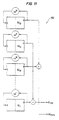
Circuit 448 of Fig. 10 includes means for calculating error evaluator polynomial W(x). As embodied herein, the means for computing the values of error evaluator polynomial W(x) comprises w registers 450, amend syndrome 54registers 210, error located polynomial NU registers 352,multiplier 350, and treedadder 354 which executes the procedure shown in Fig. 3, including, specifically step 106. For simplicity, the calculation is shown instep 106 in an inverse form. The coefficients of W'(x) are the coefficients of W(x) only in reverse order. To illustrate:
NU registers 352 and SY registers 210 to GF multiple 350 and tree'd .XOR. function 354 throughout computation of W(x). Tenbit bus 356 is connected to register W(31) of W(I) shift registers 450. - Starting with a
new state 1, the products of SY and NU are multiplied byGF multiplier 350 and are tree .XOR.'d bydevice 354, the operation of which have both been described hereinabove. A single 10 bit symbol is input to register W(31) frombus 356. Duringstate 2, the contents of all W(I) registers are input to all W(I-1) registers via 32 ten bit symbol busses 452 (downshifting the W values) and all SY(I) values are shifted to SY(I+1) (upshifting the SY(I) values).States Registers - The circuits of Fig. 13 provide the means for simultaneously solving the error locator polynomial NU(x), for obtaining the corresponding error value from NU(x) and W(x), and for correcting erroneous symbols in code word y(x) to error free symbols ai as each symbol is shifted out of
buffer 22 of Fig. 1, which includes the steps of (1) solving each term of NU(x), summing the odd and even power terms into NUodd(x) and NUeven(x) respectively, step 108 of Fig. 3, (2) simultaneously evaluating W(x), and (3) correcting errors in y(x) as indicated by the error locations and error values derived from the calculated values of NUodd(x) and W(x). In order to generate a correction symbol, or correction vector YI, which is non-zero coefficient of p(x) for a given code word symbol, the errorvalue computation circuit 20 of Fig. 1 evaluates the 32 symbol values of NU(x) plus the lowest order coefficient of NU(x) which is always 1, and the 32 symbol values of W(x) for each code word symbol within the sector in real time at the same time as the corresponding symbol is shifted out ofbuffer 22 of Fig. 1. The results of these evaluations are then manipulated to generate the actual correction polynomial p(x). - To determine error locations, the usual practice is to use a Chien search, where all possible legitimate values of x are tested to find the roots of NU(x). Based on those roots, the erroneous symbols are identified, W(x) evaluated, and y(x) later corrected. However, the standard technique requires more latency than the present invention. To provide the advantage of low latency, the Chien search is modified to permit simultaneous evaluation of W(x), data flow is pipelined, and erroneous symbols are identified and corrected in real time as they exit
buffer 22 of Fig. 1 on their way todata processing bus 28. This requires a Chien search as modified by the present invention to compute the value of NU(x) and W(x) as each symbol exitsbuffer 22, whereupon a decision is made as to whether the symbol is incorrect. If incorrect, the non-zero coefficient in p(x), computed from NU(x) and W(x), amends the erroneous symbol in .XOR.circuit 24. -
Circuit 480 of Fig. 11, consisting of a plurality of Galois Field multiplier means, each containing a 10 bit shift register and a Galois Field multiplier network, evaluates NU (αi) as each code symbol is timed to exitbuffer 22 of Fig. 1, where i is the number of thesymbol exiting buffer 22 of Fig. 1. During each clock cycle, the contents of each NU register NU1 to NU32 is multiplied by the GF multiplier connected to the register, thereby testing for a root αi of NU for each clock cycle. The contents of each NU register ofcircuit 480 is multiplied by its corresponding GF multiplier once for each corresponding data symbol. Values of NU for the even powers of x and values of NU for the odd powers of x are summed separately and are referred to as NUeven and NUodd. This completessteps circuit 500 of Fig. 12 once for eachsymbol exiting buffer 22. In particular,circuit 500 of Fig. 12 computes W (αi) x α34i for each symbol, corresponding to step 116 of Fig. 3. - Looking to Fig. 13,
circuit 480 is the same circuit as shown in Fig. 11, andcircuit 500 is the same circuit as shown in Fig. 12.Summer 520 computes NU(x) as the sum of NUodd and NUeven. If NU(x) = 1 then the ith symbol of the codeword exiting buffer 22 is in error, andgate 522 enables one input ofgates divider circuit 524 computes the correct value, or correction vector of the ith code word symbol. This is shown as YI in step 116 of Fig. 3 and will be discussed in more detail hereinbelow. Also at the same time,logic gate 526 checks for NUodd = 0. If it is zero and NUeven = 1, thengate 528 sets a system flag indicating todata processing system 28 of Fig. 1 that the decoded output ofcircuit 10 is erroneous. The disposition of the erroneous data is let up to the data processing system. Also, if NUodd = 0, correction vector YI will not be gated to .XOR.circuit 24 becausegate 530 of Fig. 13 will be locked open. This corresponds to step 118 of Fig. 3. An error location found while NUodd = 0 indicates a malfunction of the decoding process. -
Divider circuit 524 of Fig. 13, shown in greater detail in Fig. 14, operates in a similar manner to the GF inverse circuit of Fig. 9 except that a second input and third multiplier have been added.Divider 524 calculates the correction vector YI, step 116 of Fig. 3, by dividing Z fromstep 114, which is represented by symbol αm of Fig. 14, by NUodd, which is represented by symbol αn of Fig. 14. The resulting correction vector is therefore:
-
Circuit 24 of Fig. 1 amends erroneous code word symbols by .XOR.ing the data stream frombuffer 22 with the correction vectors, step 122 of Fig. 3. When a symbol is not in error,gate 530 of Fig. 13 is open and the correction vector is zero, therefore .XOR.circuit 24 leaves the data symbol unchanged. The buffer data stream must be synchronized with the computation of error values so that the correction vectors match the correct data symbols. -
Buffer circuit 22 of Fig. 1 is a large first-in-first-out storage unit for data read fromdisk data port 26 and provides data to amendcircuit 24 approximately 2 sector times following data entry to the buffer. In the preferred embodiment the input symbols are latched into a shift register once for each symbol read time, generating a 30 bit word. Each group of 3 symbols shifted in is written to a holding register, then later transferred into the buffer where the group remains until the end of the two sector delay time, whereupon the group of 3 symbols is received by a read shift register and sent to the data amendfunction 24 of Fig. 1, one symbol at a time. - The final function performed by the decoding circuitry is conversion of the amended 10 bit symbols into 16 bit data words and EDC words by
converter 27 of Fig. 1. Bits 0-9 of the first data word are bits 0-9 of the first symbol. Bits 10-15 of the second data word are bits 0-5 of the second symbol. Conversion continues for all data words so that bits 0-7 of symbol 413 are bits 8-15 of the last data word, andbits - In describing the operation of
circuit 10 of Fig. 1, reference is made to Fig. 15 which shows the time allocations for major data shifts and computations performed by the encoding and decoding circuits. The data flow between sections ofcircuit 10 is unidirectional, that is, there is no handshaking. Each section is ready to accept new data when the previous section is ready to supply it. The chip manipulates data in a synchronous manner, having one single clock source. The cycle time of the clock in the preferred embodiment is nominally 70 ns which is half-symbol time. A full symbol time in the preferred embodiment is 140 ns. - Decoding commences with data symbols being read from the
data storage device 26 intobuffer 22 andsyndrome computer 16 of Fig. 1,time slots time slot 604 are also read intosyndrome computer 16.Buffer 22 holds data read duringtime slot 600 for approximately two sector times and does not release the data untiltime slot 606. As data intime slot 602 are being read intosyndrome computer 16 of Fig. 1, the syndrome computer begins processing data duringtime slot 608. Following syndrome and amend syndrome computation, error evaluator polynomial W and error locator polynomial NU are computed duringtime slots buffer 22 in time slow 606. - After the syndrome computation during
time slot 608 is complete,syndrome computer 16 is now ready to begin computations on the next code word attime slot 616, with syndromes for these data being computed during time slot 618, and error evaluator and error locator polynomials being computed during time slots 620 and 622 respectively. Correction vectors duringtime slot 624 are calculated for the data oftime slot 616 as they are released frombuffer 22 duringtime slot 626. - This timing diagram clearly shows the pipelining made possible by the improved algorithms and circuits of the present invention.
- In a second preferred embodiment, a savings is made in hardware in the exclusive OR (.XOR.) networks used to implement the GF xαi multiplications shown in Fig. 4 for the syndrome computer, Fig. 12 or Fig. 13 for the error evaluator polynomial W(x) computer, and Fig. 11 or Fig. 13 for the NUodd and NUeven computers. To implement the zαi multipliers of the present invention, it is necessary to build an .XOR. network, such as the α-33 multiplier shown in Fig. 16. The ⊕ symbols are .XOR. gates. The input is a 10 bit symbol [SYMBOL A] and the output is a 10 bit symbol [SYMBOL A] xα-33.
- The size of this kind of .XOR. network is large, requiring 59 .XOR. gates for the α-33 multiplier of Fig. 16, and 60 .XOR. gates for the α-32 multiplier of Fig. 17. These large .XOR. networks are complex to implement at the VLSI level, therefore, it is difficult to build many of them in a small silicon integrated circuit. The second preferred embodiment of the present invention provides an improved Galois Field multiplier means which reduces the number and complexity of these GF multiplier circuits.
- On the Galois Field, αi xαj = αi+j. For example, α-32 may be generated by multiplying α-33 by α1. A given a multiplier may therefore be constructed from products of simpler multipliers. The circuit of Fig. 18 shows an α1 multiplier circuit, or Shift-1 circuit, which uses one .XOR. gate to perform a modulo-2 addition (
bit 9 .XOR. bit 2) to generate theoutput bit 3 and also uses some cross-connected input and output lines to transpose bits to provide the desired output. The circuit of Fig. 19 shows an α2 multiplier circuit, or Shift-2 circuit, consisting of two .XOR. gates and cross-connected inputs and outputs to produce the desired output. The circuits of Fig. 20a and 20b show how the product of a complex α multiplier, α-33 or α30, and a simple multiplier, α1 or α2 can produce an output that ordinarily would require two complex multipliers, thereby considerably reducing circuit complexity. In Fig. 20a, an α-33 and an α1 multiplier produce an output consisting of the input symbol [SYMBOL A] times α-33 and also times α-32 for a net savings of 59 .XOR. gates, or one α-32 multiplier network. Similarly, as shown in Fig. 20b, the values of [SYMBOL B]Xα30 and [SYMBOL B] xα32 are generated using a α30 multiplier and a Shift-2 circuit, thereby eliminating an α32 multiplier. - The application of this technique to the GF multiplier means for the present invention eliminates almost half of the complex .XOR. networks required by the syndrome computer and error location and error evaluator computers. Fig. 21 shows the syndrome computer of Fig. 4 configured according to the second preferred embodiment to exploit the technique of reducing the complexity of the GF multipliers. To simplify the drawings, only the S(-30) to S(-33) registers and related GF multiplier and multipliers (MUXes) are shown and described; the rest being repetitive. The function of the syndrome computers has already been described hereinabove. Only the application of the GF multiplier means hardware reduction techniques to the syndrome computer will now be discussed.
-
Syndrome computer 16 of Fig. 1 processes one symbol through the syndrome compute circuit of fig. 4 or Fig. 21 approximately every 140 ns (a full symbol clock) in both preferred embodiments. In the second preferred embodiment of the syndrome computer circuit as shown in Fig. 21, the syndrome compute circuit consists of a plurality of Galois Field multiplier means each comprising two 10-bit registers coupled to modulo-2 adder by a 2-to-1 multiplexer, a hold register, a complex GF multiplier .XOR. network, and a simple Shift-1 multiplexer. - Before
syndrome computer 16 begins doing calculations, all S registers, 702, 704, 706, and 708 of Fig. 21, are cleared by a signal onreset line 738. During the first half symbol clock or approximately 70 ns, the 2-to-1 multiplexers (2-to-1 MuXes) 710 and 712 are enabled to allow the contents in the odd numbered S registers, S(-33), S(-31), etc. to modulo-2 add their contents by GF addition inadders disk 26 of Fig. 1. The resulting sums are stored in hold registers 718 and 720. The contents of the hold registers are next multiplied by the GF multipliers, α-31 and α-33, 722 and 724, and the resulting product is loaded into S(-31) and S(-33) registers 704 and 708. The contents of S(-31)register 704 are [(previous S(-31) register contents) + (data symbol from disk 26)] x α-31, and the contents of S(-33)register 708 are: [(previous S(-33) register contents) + (data symbol from disk 26)] xα-33. - In the next half symbol clock of approximately 70 ns, the 2-to-1
MUXes disk 26 inadders circuits registers register 702 are [(previous S(-30) register contents + (data symbol from disk 26)] xα-30 and the contents of S(-32)register 706 are [(previous S(-32) register contents) + (data symbol from disk)] xα-32. This add and multiply calculation is repeated for the next ten-bit data symbol retrieved from the disk. - In the first preferred embodiment of the syndrome computer, an output value of S is provided from the output of each adder associated with each S register as shown in Fig. 4. In the second preferred embodiment, one output line, for example 730 of Fig. 21, provides the output for two S registers, 706, 708. One value of S is output every half symbol clock to multiplexer 732 which directs the symbol to its respective S' register of Fig. 5 via
lines 734 and 736. - Figs. 22a and 22b show the error locator polynomial NU(x)
computer circuit 480 of Fig. 11 or Fig. 13 for computing NUodd and NUeven configured to according to the second preferred embodiment to exploit the technique of reducing the complexity of the GF multipliers. Figs. 22a and 22b show only small portions of the computers to illustrate the implementation of the technique. The circuits of Figs. 22a and 22b perform the same functions as theequivalent circuits 480 of Fig. 11 or Fig. 13 in the first preferred embodiment, therefore the function of these circuits will not be discussed further. Only the application of the GF multiplier hardware reduction techniques to the error locator computer will not be discussed. - In the second preferred embodiment as shown in Figs. 22a and 22b, the NUeven and NUodd computer consists of a plurality of Galois Field multiplier means, each comprising two 10-bit shift registers coupled to a hold register by a 2-to-1 multiplexer, a complex GF multiplier .XOR. network, and a simple Shift-2 multiplier for repetitively multiplying the contents of the shift registers by a value of αi. Before the NU calculators start doing calculations, a set of ten-bit symbol values are loaded into all NU even numbered
registers 750, 752 (only a representative two of which are labeled) and all NU odd numberedregisters 771, 773 (only a representative two of which are labeled) frombus 456 connection now shown). During the first half symbol clock of approximately 70ns the 2-to-1MUXes GF multipliers register 750 is now equal to [previous NU(30) register contents] α30 and the contents of NU(29)register 771 is [previous NU(29) register contents]Xα29. - During the next half symbol clock the 2-to-1
MUXes GF multipliers circuits register 752 is equal to [previous NU(32) register contents] xα31. This process is again repeated in the next symbol clock. - Fig. 23 shows the error evaluator polynomial W(x)
computer circuit 500 of Fig. 12 or Fig. 13, configured to according to the second preferred embodiment to exploit the technique of reducing the complexity of the GF multipliers. Fig. 23 shows only a small portion of the computer to illustrate the implementation of the technique. The circuit of Fig. 23 performs the same functions as theequivalent circuit 500 of Fig. 12 or Fig. 13 in the first preferred embodiment, therefore, the function of this circuit will not be discussed further. Only the application of the GF multiplier hardware reduction techniques to the error evaluator computer will now be discussed. -
Error evaluator circuit 800 consists of a plurality of Galois Field multiplier means, of the same form as the NUodd and NUeven circuits of Figs. 22a and 22b, for repetitively multiplying the contents of the NU registers by αi, and functions in a similar manner. Even values of W() are calculated and stored in the even W registers during one half symbol clock and odd values are calculated and stored in the odd W registers during the next half symbol clock. Only even numbered α multipliers are provided; the odd α multipliers are provided by the shift-1 circuit. - Because only half of the W values are calculated and summed in treed
adder 802 during each half symbol clock,accumulator 804 stores and adds the even and odd outputs ofadder 802 to provide the full value of W() for computation of the correction vector as shown on Fig. 13. - By applying the technique of the second preferred embodiment to the syndrome computer, only 34 complex GF multiplier .XOR. networks are required rather than the 67 required to implement the algorithm in hardware in the first preferred embodiment. Likewise, this technique reduces the need for .XOR networks in the NUeven, NUodd, and W computers from 64 to 32.
- Additional advantages and modifications will readily occur to those skilled in the art. The invention it its broader aspects is, therefore, not limited to the specific details, representative apparatus and illustrative examples shown and described. Accordingly, departures may be made from such details without departing from the scope of applicants' general inventive concept as defined in the appended claims.
Claims (22)
- Apparatus for detecting and correcting errors in binary data symbols which have been encoded using a Reed-Solomon error correction code to produce Reed-Solomon code words, wherein each code word includes in it a selected number of data symbols, said apparatus comprising :A. buffer means (22) for receiving at least one code word having the selected number of data symbols and releasing each of the received data symbols after a preselected time period;B. decoder means (16,18 and 20) for computing, for each received code word, error locations and error values by (i) determining an error locator equation and finding roots of said error locator equation, the roots corresponding to error locations, and (ii) determining associated error values, andC. correcting means (22 and 24), responsive to the computed error locations and error values, for correcting each of the received data symbols having an error upon release of the symbol from the buffer means,the decoder means being further characterized as :
including a plurality of Galois Field multiplier means for repetitively multiplying signals associated with said received code words by αi, each of said Galois Field multiplier means comprising:1. a multiplexer (710,754 or 775) for passing a first input signal during a first predetermined time interval and a second input signal during a second predetermined time interval to obtain a first output signal;2. a first Galois Field multiplier (722,758 or 779) for multiplying the first output signal by a first predetermined value to produce a second output signal;3. a first register (704,750 or 771) coupled to provide the first input signal to the multiplexer and to store the resulting second output signal during the first predetermined time interval;4. a second Galois Field multiplier (726,762 or 783) for multiplying the second output signal by a second predetermined value to produce a third output signal; and5. a second register (702,752 or 773) coupled to provide the second input signal to the multiplexer and store the resulting third output signal during the second predetermined time interval;wherein said decoder means combines at predetermined time the contents of selected ones of said first and second registers and uses the combinations in determining the error locations and associated error values. - The apparatus of claim I wherein said decoder means further includes computing means for computing syndromes Si for each of said received code words as the code word data symbols are received, the computing means comprising:i. a plurality of S computers for generating the coefficients Si of a syndrome polynomial S(x); andii. an amend syndrome calculator (200) for amending the coefficients of S(x) to correspond to a shortened code.
- The apparatus of claim 2 wherein the decoder means includes means for simultaneously computing, from the amended coefficients, the values of an error locator polynomial NU(x) associated with the error locator equation and an error evaluator polynomial W(x) for each of the received data symbols where :

- The apparatus of claim 3 wherein said decoder means further includes :A. means (480,500) for simultaneously evaluating NUodd(αi), NUeven(αi) and W(αi) corresponding to each received data symbol as that symbol is released from said buffer, where αi corresponds to a code word location, and NUeven(αi) and NUodd(αi) are the sums of the even and odd terms, respectively, of the error locator polynomial calculated at αi: andB. means (522,524) for simultaneously evaluating an expression NUodd(αi) + NUeven(αi) and calculating a correction vector YI corresponding to each of said received data symbols, where :

- The apparatus of claim 2 wherein each S computer includes a Galois Field multiplier means for repetitively multiplying input signals associated with the syndromes by αi, the multiplier means comprising :a. a logical AND circuit (152) responsive to a feedback signal and an input signal for providing a first output signal;b. a Galois Field multiplier (xαi) responsive to the first output signal for multiplying the first output signal by a predetermined value at a predetermined time to obtain a second output signal;c. a storage register (Si) for storing the second output signal; andd. a Galois Field adder for adding the stored second output signal to a data signal and providing the sum as the input signal to the logical AND circuit (152).
- The apparatus of claim 2 wherein each S computer includes a Galois Field multiplier means for repetitively multiplying a signal by αi, the Galois Field multiplier means comprising:A. a multiplexer (710) for passing a first input signal during a first predetermined time interval and a second input signal during a second predetermined time interval to obtain a first output signal;B. modulo-2 adder (714) means for adding the first output signal to a data signal to obtain a second output signal;C. a first Galois Field multiplier (722) for multiplying the second output signal by a first predetermined value to produce a third output signal;D. a first register (704) coupled to provide the first input signal to the multiplexer and to store the third output signal during the first predetermined time interval;E. a second Galois Field multiplier (726) for multiplying the third output signal by a second predetermined value to produce a fourth output signal; andF. a second register (702) coupled to provide the second input signal to the multiplexer and to store the fourth output signal during the second predetermined time interval;wherein, after a predetermined number of repetitions, the contents of said first and second registers correspond to the coefficients Si of the syndrome polynomial S(x).
- The apparatus of claim 3 wherein the means (480) for computing the values of the error locator polynomial NU(x) includes Galois Field multiplier means for repetitively multiplying signals associated with coefficients of NU(x) by αi, the multiplier means comprising :A. storage means having an input port and an output port, the input port receiving an input signal for storage and the output port supplying the stored signal as an output signal; andB. a Galois Field multiplier to recursively generate the input signal by multiplying the output signal by a predetermined value.
- The apparatus of claim 3 wherein the means (500) for computing the values of an error evaluator polynomial W(x) includes a plurality of Galois Field multiplier means for repetitively multiplying signals associated with coefficients of W(x) by αi, each of said Galois Field multiplier means comprising:A. storage means having an input port and an output port, the input port receiving an input signal for storage and the output port supplying the stored signal as an output signal; andB. a Galois Field multiplier to recursively generate the input signal by Galois Field multiplying the output signal at a predetermined time.
- The apparatus of claim 1 wherein the first and second registers contain, after a predetermined number of repetitions, signals associated with coefficients Si of a syndrome polynomial S(x).
- The apparatus of claim 9 wherein said decoder further includes a Galois Field adder (714) for adding a data signal to the output of the multiplexer (710) to produce the first output signal.
- The system of claim 1 wherein the first and second registers contain, after a predetermined number of repetitions, signals associated with coefficients of an error evaluator polynomial W(x).
- The system of claim 1 wherein the first and second registers contain, after a predetermined number of repetitions, signals associated with coefficients of an error evaluator polynomial NU(x).
- A method for detecting and correcting errors in binary data symbols, which have been encoded using a Reed-Solomon error correction code to produce Reed-Solomon code words, wherein each code word includes in it a selected number of data symbols, said method comprising the steps of:A. receiving at least one code word having the selected number of data symbols and holding each of the received data symbols in a buffer for a preselected time period;B. computing for each received code word error locations and error values by (i) determining an error locator equation and finding roots of the error locator equation, the roots corresponding to error locations, and (ii) determining associated error values;C. releasing each of the received data symbols from the buffer after the preselected time period; andD. correcting, in response to the computed error locations and associated error values, each of the received data symbols having an error when the symbol is released from the buffer,wherein said computing step is further characterized by repetitively Galois Field multiplying , by αi, signals associated with said received code words by performing the steps of --1. passing in a multiplexer a first input signal during a first predetermined time interval and a second input signal during a second predetermined time interval to obtain a first output signal;2. multiplying in a Galois Field multiplier the first output signal by a first predetermined value to produce a second output signal;3. storing in a first register the second output signal during the first predetermined time interval;4. multiplying in a Galois Field multiplier the second output signal by a second predetermined value to produce a third output signal;5. storing in a second register the third output signal during the second predetermined time interval;6. coupling the stored second output signal to the multiplexer during the first predetermined time interval;7. coupling the stored third output signal to the multiplexer during the second predetermined time interval; and8. manipulating at predetermined times the contents of selected ones of said first and second registers to determine error locations and error values corresponding to the received code words.
- The method of claim 13 wherein said step of computing the error locations and the error values includes :a. computing syndromes Si for each of the received code words as the code word data symbols are received;b. simultaneously computing the values of an error locator polynomial NU(x) and an error evaluator polynomial W(x) for each of the received code words, where :S(x) is a polynomial in x with coefficients Si, t is the number of errors that the Reed-Solomon code can correct and NU(x) is associated with the error locator equation.

- The method of claim 13, wherein said step of computing error locations and error values includes the steps of :a. simultaneously evaluating NUodd(αi), NUeven(αi) and W(αi) corresponding to each received data symbol as that symbol is released from said buffer, where αi corresponds to a code word location, and NUeven(αi) and NUodd(αi) are the sums of the even and odd terms, respectively, of the error locator polynomial calculated at αi; andb. simultaneously evaluating an expression NUodd(αi) + NUeven(αi) and calculating a correction vector YI corresponding to each of said received data symbols, where:

- The method of claim 14 wherein the step of computing syndromes comprises :a. generating the coefficients Si of a syndrome polynomial S(x) in a plurality of S computers; andb. amending the coefficients of S(x) to correspond to a shortened code over Galois Field (2m).
- The method of claim 16 wherein the step of generating the coefficients of the syndrome polynomial S(x) comprises:a. providing a first output signal from a logical AND circuit responsive to a feedback signal and an input signal;b. multiplying, in a Galois Field multiplier, the first output signal by a predetermined value at a predetermined time to obtain a second output signal;c. storing the second output signal in a storage register; andd. adding the stores second output signal to a data signal in a modulo-2 adder and providing the sum as the input signal to the logical AND circuit.
- The method of claim 16 wherein the step of generating coefficients Si of the syndrome polynomial S(x) includes the steps of :i. passing, in a multiplexer, a first input signal during a first predetermined time interval and a second input signal during a second predetermined interval time to obtain a first output signal;ii. adding the first output signal to a data signal in a modulo-2 adder to obtain a second output signal;iii. multiplying, in a Galois Field multiplier, the second output signal by a first predetermined value to produce a third output signal;iv. storing the third output signal during the first predetermined time interval in a first register;v. Galois Field multiplying, in a Galois Field multiplier, the third output signal by a second predetermined value to produce a fourth output signal;vi. storing the fourth output signal during the second predetermined time interval in a second register;vii. coupling the stored third output signal to the multiplexer during the first predetermined time interval;viii. coupling the stored fourth output signal to the multiplexer during the second predetermined time interval; andix. repeating steps i-viii a predetermined number of times;wherein said first and second registers contain, after the predetermined number of repetitions. signals associated with the syndrome coefficients Si.
- The method of claim 13 wherein the step of computing the value of an error evaluator polynomial W(x) includes Galois Field multiplying comprising :A. storing an input signal in a storage means having an input port for receiving input signals and an output port for supplying stored input signals as output signals; andB. recursively multiplying the output signals by a Galois Field multiplier to generate the input signals.
- The method of claim 13 wherein the step of computing the value of an error evaluator polynomial W(x) includes Galois Field multiplying by αi signals associated with a received code word, and Galois Field multiplying includes the steps of :i. passing in a multiplexer a first input signal during a first predetermined time interval and a second input signal during a second predetermined interval time to obtain a first output signal;ii. multiplying in a Galois Field multiplier the first output signal by a first predetermined value to produce a second output signal;iii. storing the second output signal during the first predetermined time interval in a first register;iv. multiplying in a Galois Field multiplier the second output signal by a second predetermined value to produce a fourth output signal;v. storing the fourth output signal during the second predetermined time interval in a second register;vi. coupling the stored third output signal to the multiplexer during the first predetermined time interval;vii. coupling the stored fourth output signal to the multiplexer during the second predetermined time interval; andviii. repeating steps i-vii a predetermined number of times;wherein, after a predetermined number of repetitions, said first and second registers contain signals which are associated with the coefficients of the error evaluator polynomial.
- The apparatus of claim 1, in which the decoder means (16,18,20) further includes:A. means for retrieving code words;B. means (16) for decoding code words and determining corresponding syndromes;C. means (18) for determining said error locator equation based on the syndromes; andD. error evaluation means (18) for finding said roots of the error locator equation and said error values associated with the error locations.E. said means for determining said error locator equation iteratively determining, in a predetermined number of iterations, said an error locator equation, and including:i. means for determining a preliminary error locator equation based on said syndromes,ii. means for iteratively updating the preliminary error locator equation following a given iteration, if the value of a particular variable is within a predetermined value range, andiii. means for updating the value of the particular variable in each iteration by incrementing the variable, said means changing the sign of the particular variable if a second particular variable has a predetermined value.
- The decoder of claim 21, wherein said means for updating the preliminary error location equation uses the Berlekamp-Massey method to determine a next value for the preliminary error locator equation.
Applications Claiming Priority (5)
| Application Number | Priority Date | Filing Date | Title |
|---|---|---|---|
| US8837887A | 1987-08-24 | 1987-08-24 | |
| US88378 | 1987-08-24 | ||
| US13620687A | 1987-12-21 | 1987-12-21 | |
| US136206 | 1987-12-21 | ||
| PCT/US1988/002898 WO1989002123A1 (en) | 1987-08-24 | 1988-08-23 | High bandwidth reed-solomon encoding, decoding and error correcting circuit |
Publications (3)
| Publication Number | Publication Date |
|---|---|
| EP0329775A1 EP0329775A1 (en) | 1989-08-30 |
| EP0329775A4 EP0329775A4 (en) | 1991-09-25 |
| EP0329775B1 true EP0329775B1 (en) | 1997-10-01 |
Family
ID=26778593
Family Applications (1)
| Application Number | Title | Priority Date | Filing Date |
|---|---|---|---|
| EP88908530A Expired - Lifetime EP0329775B1 (en) | 1987-08-24 | 1988-08-23 | High bandwidth reed-solomon encoding, decoding and error correcting circuit and method |
Country Status (4)
| Country | Link |
|---|---|
| EP (1) | EP0329775B1 (en) |
| DE (1) | DE3856035T2 (en) |
| SG (1) | SG64886A1 (en) |
| WO (1) | WO1989002123A1 (en) |
Families Citing this family (9)
| Publication number | Priority date | Publication date | Assignee | Title |
|---|---|---|---|---|
| JPH04315332A (en) * | 1991-04-15 | 1992-11-06 | Hitachi Ltd | Error correction device |
| DE4140018A1 (en) * | 1991-12-04 | 1993-06-09 | Bts Broadcast Television Systems Gmbh, 6100 Darmstadt, De | METHOD AND CIRCUIT FOR DECODING RS-CODED DATA SIGNALS |
| US5414719A (en) * | 1992-04-24 | 1995-05-09 | Sharp Kabushiki Kaisha | Operating circuit for galois field |
| JPH08106733A (en) * | 1994-10-07 | 1996-04-23 | Hitachi Ltd | Information storage-medium utilization system |
| US6012839A (en) * | 1995-06-30 | 2000-01-11 | Quantum Corporation | Method and apparatus to protect data within a disk drive buffer |
| AU3185299A (en) * | 1998-03-12 | 1999-09-27 | Tiernan Communications, Inc. | Universal reed-solomon coder-decoder |
| GB2372680B (en) * | 2001-02-27 | 2003-02-19 | 3Com Corp | Calculation and transmission of error check codes |
| US7693927B2 (en) | 2003-08-25 | 2010-04-06 | Jennic Limited | Data processing system and method |
| CN115632662B (en) * | 2022-12-20 | 2023-04-11 | 苏州联讯仪器股份有限公司 | Syndrome calculation method, device, equipment and medium in RS decoding |
Citations (1)
| Publication number | Priority date | Publication date | Assignee | Title |
|---|---|---|---|---|
| EP0114938A2 (en) * | 1982-12-29 | 1984-08-08 | International Business Machines Corporation | On-the-fly multibyte error correction |
Family Cites Families (7)
| Publication number | Priority date | Publication date | Assignee | Title |
|---|---|---|---|---|
| US3668631A (en) * | 1969-02-13 | 1972-06-06 | Ibm | Error detection and correction system with statistically optimized data recovery |
| US4099160A (en) * | 1976-07-15 | 1978-07-04 | International Business Machines Corporation | Error location apparatus and methods |
| US4410989A (en) * | 1980-12-11 | 1983-10-18 | Cyclotomics, Inc. | Bit serial encoder |
| US4413339A (en) * | 1981-06-24 | 1983-11-01 | Digital Equipment Corporation | Multiple error detecting and correcting system employing Reed-Solomon codes |
| US4584686A (en) * | 1983-12-22 | 1986-04-22 | Optical Storage International | Reed-Solomon error correction apparatus |
| US4866716A (en) * | 1987-05-15 | 1989-09-12 | Digital Equipment Corporation | Real-time BCH error correction code decoding mechanism |
| EP0296828A3 (en) * | 1987-06-22 | 1991-06-05 | Sony Corporation | Method and apparatus for decoding reed-solomon code |
-
1988
- 1988-08-23 WO PCT/US1988/002898 patent/WO1989002123A1/en active IP Right Grant
- 1988-08-23 EP EP88908530A patent/EP0329775B1/en not_active Expired - Lifetime
- 1988-08-23 SG SG1996004948A patent/SG64886A1/en unknown
- 1988-08-23 DE DE3856035T patent/DE3856035T2/en not_active Expired - Fee Related
Patent Citations (1)
| Publication number | Priority date | Publication date | Assignee | Title |
|---|---|---|---|---|
| EP0114938A2 (en) * | 1982-12-29 | 1984-08-08 | International Business Machines Corporation | On-the-fly multibyte error correction |
Also Published As
| Publication number | Publication date |
|---|---|
| WO1989002123A1 (en) | 1989-03-09 |
| SG64886A1 (en) | 1999-05-25 |
| DE3856035T2 (en) | 1998-02-26 |
| EP0329775A4 (en) | 1991-09-25 |
| EP0329775A1 (en) | 1989-08-30 |
| DE3856035D1 (en) | 1997-11-06 |
Similar Documents
| Publication | Publication Date | Title |
|---|---|---|
| US5107503A (en) | High bandwidth reed-solomon encoding, decoding and error correcting circuit | |
| US4868828A (en) | Architecture for time or transform domain decoding of reed-solomon codes | |
| US4782490A (en) | Method and a system for multiple error detection and correction | |
| US6374383B1 (en) | Determining error locations using error correction codes | |
| Lee | High-speed VLSI architecture for parallel Reed-Solomon decoder | |
| US5170399A (en) | Reed-Solomon Euclid algorithm decoder having a process configurable Euclid stack | |
| EP0154538B1 (en) | Parity and syndrome generation for error and correction in digital communication systems | |
| EP0365555B1 (en) | Method and apparatus for error correction | |
| US5642367A (en) | Finite field polynomial processing module for error control coding | |
| US7080310B2 (en) | Forward error corrector | |
| US4873688A (en) | High-speed real-time Reed-Solomon decoder | |
| US5440570A (en) | Real-time binary BCH decoder | |
| US4504948A (en) | Syndrome processing unit for multibyte error correcting systems | |
| KR920000828B1 (en) | Galois field arithmetimetic logic unit | |
| US6571368B1 (en) | Systolic Reed-Solomon decoder | |
| US6209115B1 (en) | Reed-Solomon decoder and VLSI implementation thereof | |
| US5535225A (en) | Time domain algebraic encoder/decoder | |
| US5805617A (en) | Apparatus for computing error correction syndromes | |
| US8201061B2 (en) | Decoding error correction codes using a modular single recursion implementation | |
| EP1589665B1 (en) | Error correction decoder comprising an erasure correcting Reed-Solomon decoder and a CRC decoder | |
| EP0329775B1 (en) | High bandwidth reed-solomon encoding, decoding and error correcting circuit and method | |
| EP1502356B1 (en) | A method of soft-decision decoding of reed-solomon codes | |
| US5471485A (en) | Reed-solomon decoder using discrete time delay in power sum computation | |
| EP1102406A2 (en) | Apparatus and method for decoding digital data | |
| US6263471B1 (en) | Method and apparatus for decoding an error correction code |
Legal Events
| Date | Code | Title | Description |
|---|---|---|---|
| PUAI | Public reference made under article 153(3) epc to a published international application that has entered the european phase |
Free format text: ORIGINAL CODE: 0009012 |
|
| 17P | Request for examination filed |
Effective date: 19890428 |
|
| AK | Designated contracting states |
Kind code of ref document: A1 Designated state(s): DE FR GB IT NL |
|
| A4 | Supplementary search report drawn up and despatched |
Effective date: 19910806 |
|
| AK | Designated contracting states |
Kind code of ref document: A4 Designated state(s): DE FR GB IT NL |
|
| 17Q | First examination report despatched |
Effective date: 19940704 |
|
| RAP1 | Party data changed (applicant data changed or rights of an application transferred) |
Owner name: QUANTUM CORPORATION |
|
| GRAG | Despatch of communication of intention to grant |
Free format text: ORIGINAL CODE: EPIDOS AGRA |
|
| GRAH | Despatch of communication of intention to grant a patent |
Free format text: ORIGINAL CODE: EPIDOS IGRA |
|
| GRAH | Despatch of communication of intention to grant a patent |
Free format text: ORIGINAL CODE: EPIDOS IGRA |
|
| GRAA | (expected) grant |
Free format text: ORIGINAL CODE: 0009210 |
|
| AK | Designated contracting states |
Kind code of ref document: B1 Designated state(s): DE FR GB IT NL |
|
| REF | Corresponds to: |
Ref document number: 3856035 Country of ref document: DE Date of ref document: 19971106 |
|
| ITF | It: translation for a ep patent filed |
Owner name: NOTARBARTOLO & GERVASI S.P.A. |
|
| ET | Fr: translation filed | ||
| PGFP | Annual fee paid to national office [announced via postgrant information from national office to epo] |
Ref country code: FR Payment date: 19980720 Year of fee payment: 11 |
|
| PGFP | Annual fee paid to national office [announced via postgrant information from national office to epo] |
Ref country code: NL Payment date: 19980728 Year of fee payment: 11 |
|
| PLBE | No opposition filed within time limit |
Free format text: ORIGINAL CODE: 0009261 |
|
| STAA | Information on the status of an ep patent application or granted ep patent |
Free format text: STATUS: NO OPPOSITION FILED WITHIN TIME LIMIT |
|
| 26N | No opposition filed | ||
| PG25 | Lapsed in a contracting state [announced via postgrant information from national office to epo] |
Ref country code: NL Free format text: LAPSE BECAUSE OF NON-PAYMENT OF DUE FEES Effective date: 20000301 |
|
| PG25 | Lapsed in a contracting state [announced via postgrant information from national office to epo] |
Ref country code: FR Free format text: LAPSE BECAUSE OF NON-PAYMENT OF DUE FEES Effective date: 20000428 |
|
| NLV4 | Nl: lapsed or anulled due to non-payment of the annual fee |
Effective date: 20000301 |
|
| REG | Reference to a national code |
Ref country code: FR Ref legal event code: ST |
|
| PGFP | Annual fee paid to national office [announced via postgrant information from national office to epo] |
Ref country code: DE Payment date: 20010802 Year of fee payment: 14 |
|
| PGFP | Annual fee paid to national office [announced via postgrant information from national office to epo] |
Ref country code: GB Payment date: 20010803 Year of fee payment: 14 |
|
| REG | Reference to a national code |
Ref country code: GB Ref legal event code: IF02 |
|
| PG25 | Lapsed in a contracting state [announced via postgrant information from national office to epo] |
Ref country code: GB Free format text: LAPSE BECAUSE OF NON-PAYMENT OF DUE FEES Effective date: 20020823 |
|
| PG25 | Lapsed in a contracting state [announced via postgrant information from national office to epo] |
Ref country code: DE Free format text: LAPSE BECAUSE OF NON-PAYMENT OF DUE FEES Effective date: 20030301 |
|
| GBPC | Gb: european patent ceased through non-payment of renewal fee |
Effective date: 20020823 |
|
| PG25 | Lapsed in a contracting state [announced via postgrant information from national office to epo] |
Ref country code: IT Free format text: LAPSE BECAUSE OF NON-PAYMENT OF DUE FEES;WARNING: LAPSES OF ITALIAN PATENTS WITH EFFECTIVE DATE BEFORE 2007 MAY HAVE OCCURRED AT ANY TIME BEFORE 2007. THE CORRECT EFFECTIVE DATE MAY BE DIFFERENT FROM THE ONE RECORDED. Effective date: 20050823 |