EP0329571A1 - Demagnetization control device for a switch-mode supply with primary and secondary regulation - Google Patents
Demagnetization control device for a switch-mode supply with primary and secondary regulation Download PDFInfo
- Publication number
- EP0329571A1 EP0329571A1 EP89420014A EP89420014A EP0329571A1 EP 0329571 A1 EP0329571 A1 EP 0329571A1 EP 89420014 A EP89420014 A EP 89420014A EP 89420014 A EP89420014 A EP 89420014A EP 0329571 A1 EP0329571 A1 EP 0329571A1
- Authority
- EP
- European Patent Office
- Prior art keywords
- output
- gate
- input
- signal
- inputs
- Prior art date
- Legal status (The legal status is an assumption and is not a legal conclusion. Google has not performed a legal analysis and makes no representation as to the accuracy of the status listed.)
- Granted
Links
Images


Classifications
-
- H—ELECTRICITY
- H02—GENERATION; CONVERSION OR DISTRIBUTION OF ELECTRIC POWER
- H02M—APPARATUS FOR CONVERSION BETWEEN AC AND AC, BETWEEN AC AND DC, OR BETWEEN DC AND DC, AND FOR USE WITH MAINS OR SIMILAR POWER SUPPLY SYSTEMS; CONVERSION OF DC OR AC INPUT POWER INTO SURGE OUTPUT POWER; CONTROL OR REGULATION THEREOF
- H02M3/00—Conversion of dc power input into dc power output
- H02M3/22—Conversion of dc power input into dc power output with intermediate conversion into ac
- H02M3/24—Conversion of dc power input into dc power output with intermediate conversion into ac by static converters
- H02M3/28—Conversion of dc power input into dc power output with intermediate conversion into ac by static converters using discharge tubes with control electrode or semiconductor devices with control electrode to produce the intermediate ac
- H02M3/325—Conversion of dc power input into dc power output with intermediate conversion into ac by static converters using discharge tubes with control electrode or semiconductor devices with control electrode to produce the intermediate ac using devices of a triode or a transistor type requiring continuous application of a control signal
- H02M3/335—Conversion of dc power input into dc power output with intermediate conversion into ac by static converters using discharge tubes with control electrode or semiconductor devices with control electrode to produce the intermediate ac using devices of a triode or a transistor type requiring continuous application of a control signal using semiconductor devices only
- H02M3/33561—Conversion of dc power input into dc power output with intermediate conversion into ac by static converters using discharge tubes with control electrode or semiconductor devices with control electrode to produce the intermediate ac using devices of a triode or a transistor type requiring continuous application of a control signal using semiconductor devices only having more than one ouput with independent control
-
- H—ELECTRICITY
- H02—GENERATION; CONVERSION OR DISTRIBUTION OF ELECTRIC POWER
- H02M—APPARATUS FOR CONVERSION BETWEEN AC AND AC, BETWEEN AC AND DC, OR BETWEEN DC AND DC, AND FOR USE WITH MAINS OR SIMILAR POWER SUPPLY SYSTEMS; CONVERSION OF DC OR AC INPUT POWER INTO SURGE OUTPUT POWER; CONTROL OR REGULATION THEREOF
- H02M1/00—Details of apparatus for conversion
- H02M1/0003—Details of control, feedback or regulation circuits
- H02M1/0032—Control circuits allowing low power mode operation, e.g. in standby mode
-
- Y—GENERAL TAGGING OF NEW TECHNOLOGICAL DEVELOPMENTS; GENERAL TAGGING OF CROSS-SECTIONAL TECHNOLOGIES SPANNING OVER SEVERAL SECTIONS OF THE IPC; TECHNICAL SUBJECTS COVERED BY FORMER USPC CROSS-REFERENCE ART COLLECTIONS [XRACs] AND DIGESTS
- Y02—TECHNOLOGIES OR APPLICATIONS FOR MITIGATION OR ADAPTATION AGAINST CLIMATE CHANGE
- Y02B—CLIMATE CHANGE MITIGATION TECHNOLOGIES RELATED TO BUILDINGS, e.g. HOUSING, HOUSE APPLIANCES OR RELATED END-USER APPLICATIONS
- Y02B70/00—Technologies for an efficient end-user side electric power management and consumption
- Y02B70/10—Technologies improving the efficiency by using switched-mode power supplies [SMPS], i.e. efficient power electronics conversion e.g. power factor correction or reduction of losses in power supplies or efficient standby modes
Definitions
- the present invention relates to stabilized power supplies called switching power supplies.
- a switching power supply operates as follows: a primary transformer winding receives a current which, for example, comes from a bridge of rectifiers receiving energy from the AC network. The current in the transformer is chopped by a switch (for example a power transistor) placed in series with the primary winding.
- a switch for example a power transistor
- a transistor control circuit establishes periodic slots for switching on the transistor. During the period of the slot, the passage of current is authorized; outside the slot, the passage of current is prohibited.
- an AC voltage is then collected. This is rectified and filtered to result in a direct voltage which is the direct output voltage of the switching power supply.
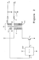
- FIG. 1 shows by way of example a switching power supply architecture manufactured by the Applicant in which two integrated circuits are used.
- One of the circuits, CI1 is used to control the base of a power transistor T p in order to apply to it periodic conduction control and blocking control signals.
- This basic control circuit CI1 is placed on the side of the primary winding (EP) of the transformer (TA).
- the other integrated circuit, regulation circuit CI2 is on the contrary placed on the side of the secondary (winding ES1) and it is used to examine the output voltage VS1 of the power supply to develop regulation signals which it transmits to the first circuit integrated through a small TX isolation transformer.
- the first integrated circuit CI1 uses these regulation signals to modify the duty cycle of conduction of the switching transistor T p and thus regulate the output voltage Vs of the power supply.
- the power supply transformer TA whose primary winding EP is supplied with A1 by an electric current coming for example from a rectifier bridge receiving energy from the alternating network.
- the other end of the primary winding EP is connected to the collector of a switching transistor Tp, the emitter of which is connected to the primary ground (shown in the figures by a black triangle).
- the transformer has several secondary windings which are preferably galvanically isolated from the mains and connected for example to a secondary electrical ground galvanically isolated from the primary ground.
- each of the secondary windings has one end connected to the secondary ground.
- the other end of each secondary winding supplies a low-pass filtering capacitor via a rectifier diode.
- a single secondary winding ES1 connected by a diode 10 to a capacitor 11.
- the direct voltage of the switching power supply is the voltage VS1 across the capacitor 11; but of course other DC output voltages can be obtained at the terminals of the other filter capacitors connected to the secondary windings by means of rectifying diodes.
- These output voltages constitute stabilized supply voltages for use circuits not shown.
- a secondary winding ES2 supplies a stabilized supply voltage of a few volts to supply the integrated regulation circuit CI2 which we have already mentioned.
- the circuit CI2 receives as input the voltage VS1, the value of which is compared with a set value applied to a pulse width modulator which establishes periodic slots of variable widths as a function of the voltage value of the output VS1; the smaller VS1, the greater the width of the slots.
- the slots are established at the switching frequency of the switching power supply. This frequency is therefore established on the secondary side of the circuit; it is generated either inside the circuit CI2, or outside in a circuit not shown, in the form of a sawtooth voltage at the selected switching frequency, connected to the circuit CI2 on a terminal 12. This sawtooth voltage is also used in known manner to effect pulse width modulation.
- the slots of variable widths produced by the regulation circuit CI2 at its output 13 are applied to a primary winding 14 of a small transformer TX whose secondary winding 15, galvanically isolated from the primary, provides pulses of variable widths. It is these pulses, of position and frequency determined by the regulation circuit CI2, which constitute the regulation signals applied to an input 16 of the control circuit CI1.
- the TX transformer consists of a few windings of winding wound on a ferrite rod, the turns of the primary and the turns of the secondary being sufficiently spaced from each other to respect the galvanic isolation standards between primary circuits and secondary circuits of the switching power supply.
- the integrated control circuit CI1 comprises means known in themselves intended to constitute at its output 17 periodic slots of variable widths faithfully reproducing the signals produced at 13 by the regulation circuit CI2. These signals produced at 17 by the circuit CI1 are applied to the base of the switching transistor Tp.
- the circuit CI1 is supplied with electric current in A3 by any known means, and is connected to the primary ground.
- Such a switching power supply device can advantageously be used in a television set.
- the sawtooth voltage applied at 12 to the circuit CI2 is synchronized with the horizontal scanning frequency so that the switching transistor Tp is turned back on when the spot returns, so that the noise generated by the switching of the transistor is not visible on the image.
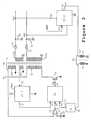
- This other regulation mode is called primary regulation because it takes place via a circuit CI3 located on the primary side.
- FIG. 2 a distinction is made, in a manner comparable to FIG. 1, of the power supply transformer TA comprising a primary winding EP supplied with rectified current and connected to the collector of a switching transistor Tp whose emitter is connected to ground. primary.
- the secondary windings ES1 and ES2 each deliver electrical currents which, after rectification and filtering, constitute power supplies which are desired to be are stabilized.
- the regulation system consists of another secondary winding ES3, one end of which is connected to the primary ground and the other end of which is connected to the input 18 of the circuit CI3.
- the voltage applied to input 18 is compared, in circuit CI3, to a set value and is applied to a pulse width modulator which establishes periodic slots of variable widths as a function of the value of the voltage applied in 18.
- the slots are established at the switching frequency of the switching power supply. This frequency is therefore established on the primary side of the circuit, it is generated in the form of a sawtooth voltage at a selected switching frequency.
- This primary regulation system has the advantage of being simpler to carry out, since it does not require the use of an auxiliary transformer TX nor of a circuit for reshaping the output signal of the transformer TX.
- Such primary regulation has the drawback of poorer regulation quality, as well as the impossibility of easily achieving synchronization between the switching frequency and another frequency resulting from the operation of a device supplied from the side.
- secondary for example of a device corresponding to the horizontal scanning of a television set.
- a switching power supply comprising both a system of primary regulation and a secondary regulation system.
- primary regulation is used when the set is in so-called standby operation
- secondary control is used when the set is in said normal operation.
- the primary regulation is adjusted so as to stabilize the supply to a value lower than that of the secondary regulation.
- one of the outputs VS1 of the stabilized supply can for example provide a voltage of 124 volts, and when the television set is in standby operation, this same output VS1 can supply a voltage close to 100 volts.
- the other outputs VS2, etc. provide voltages which vary according to the operating mode in the same proportions.
- a switching power supply is thus constituted comprising both a primary regulation and a secondary regulation, it is necessary to provide a switching power supply system comprising both the circuits as described in FIG. 1 and the circuits such as described in Figure 2.
- the base of the switching transistor Tp must be connected to both an output 17 of the circuit CI1 and an output 19 of the circuit CI3, for example via of a door OR.
- the circuit CI3 When the television set is in standby operating mode, only the primary regulation device is in operation, and the circuit CI3 alone delivers signals to the base of the switching transistor Tp.
- the primary and secondary regulation devices When the television set is in normal operating mode, the primary and secondary regulation devices are simultaneously in operation, but since the primary regulation is adjusted to stabilize a voltage lower than that of the secondary regulation, the circuit CI3 does not deliver output signals since, on its input 18, it finds a voltage greater than the setpoint voltage, and it is only the secondary regulation circuit CI2 which delivers output signals intended to control, via the circuit CI1, the base of the switching transistor Tp.
- the simultaneous presence of signals from the primary and secondary regulation circuits can cause the switching transistor Tp to turn back on at times when the demagnetization of the transformer TA is not finished; and it is known, in this case, that the switching transistor risks being damaged due to the fact that the conduction takes place when the collector is at a too high potential and that the switching transistor is, moreover , caused to pass a current greater than normal.
- the present invention relates to a device making it possible, in all circumstances, on the one hand, to ensure complete demagnetization of the power supply transformer TA between successive conductions, on the other hand, to avoid the passage of excessively large currents .
- the present invention therefore relates to a switching power supply comprising both a primary regulation system and a secondary regulation system, each of these two regulation systems being able to be led to output signals consisting of periodic slots of variable widths.
- each of these signals can take a first logic state (0) corresponding to a blocking order from a main switch and a second logic state (1) corresponding to a command to turn on this main switch.
- this switching power supply comprises: a means of comparison, with respect to a low or zero voltage value, of the output voltage of a secondary winding, the output of the comparison means delivering a signal taking the logic state 1 when the transformer of the power supply switching is demagnetized and logic state 0 when this transformer is not demagnetized, and a logic circuit receiving as input the output signal from the comparison means, the output signal from the primary regulator and the output signal from the secondary regulator, this logic circuit delivering as output a command signal from the main switch which can take a logic state 0 for blocking the main switch or a logic state 1 for switching it on, according to the following criteria: * the control signal goes to state 1 if the comparator output signal is in state 1 and if the output signal from at least one of the regulators is in state 1, * the control signal goes to state 0 when the output signal from the regulator which caused the setting of the control signal to 1 goes to state 0.
- the logic circuit comprises: - two identical flip-flop logic circuits each comprising a switching input S, a reset input R and an inverted output Q *, - a first AND gate and a second AND gate, with two inputs each, and an OR gate with two inputs, - a set of connections constituted so that the comparator output signal reaches both the inputs R of the flip-flop circuits, that the outputs of the first and second AND gates are respectively connected to the inputs S of the flip-flop circuits, that the outputs Q * of the flip-flop circuits are connected respectively to the inputs of the second and first gates AND, that the output signal of the primary regulator by comes to the other input of the first AND gate, that the output signal of the secondary regulator reaches the other input of the second AND gate, and that the outputs of the two AND gates are connected respectively to the two inputs of the OR gate whose output corresponds to the output point of the logic circuit.
- each of the flip-flop logic circuits consists of a flip-flop D, comprising inputs D, CK, an output Q, and an inverted output Q *, of an AND gate with two inputs , of an OR gate with two inputs and various connections constituted so that input D is connected to output Q *, output Q is connected to one of the inputs of gate AND, the output of gate AND is connected to one of the inputs of the OR gate and the output of the OR gate is connected to the input CK, the other input of the OR gate constituting the switching input S of one of the circuits flip-flop, the other input of the AND gate constituting the reset input R of the flip-flop circuit and the output Q * of flip-flop D constituting the same output Q * of the flip-flop circuit.
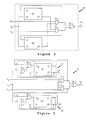
- FIG. 3 represents the power supply transformer TA comprising a primary winding EP, two secondary windings ES1 and ES2 each connected to a secondary ground, and a secondary winding ES3 connected to a primary ground.
- the primary winding EP has one end supplied with A1 by a current rectified from an alternating current from the sector, and the other end connected to the collector of the power transistor Tp whose emitter is connected to the primary ground.
- the secondary winding ES1 delivers an alternating current with respect to the secondary ground which is rectified by a diode 10 and regulated by a capacitor 11 so as to produce at output VS1 a voltage of 124 volts, when the television set is in normal operation .
- the secondary winding ES2 produces an alternating current which is rectified by a diode 20 and regulated by a capacitor 21 so as to produce an output voltage of 12 volts when the television set is in normal operation.
- the primary regulation circuit CI3 receives on its input an electrical signal coming from the output of the secondary winding ES3, is supplied with direct current in A3 and connected to a primary ground, and delivers on its output, 19, a regulation signal Pp consisting of periodic slots of variable widths as a function of the value of the output voltage VS3 of the secondary winding ES3; the smaller the VS3, the larger the width of the slots.
- a secondary regulation circuit CI2 receives as input an electrical signal coming from the supply line of 124 volts VS1, is supplied in A2 by an electric current coming from the supply line VS2 (12 volts compared to the secondary ground) , and produces at output 13 a signal Ps ′ consisting of periodic slots of variable widths as a function of the value of the voltage at line VS1; the smaller VS1, the greater the width of the slots.
- the slots are established at the switching frequency of the switching power supply. This brother quence is generated in a circuit not shown, in the form of a sawtooth voltage at the selected switching frequency, introduced into the circuit CI2 at point 12.
- a circuit CI1 receives as input 16 a signal coming from a secondary winding 15 of a transformer TX whose primary winding 14 receives the signal Ps ′ from the circuit CI2.
- the signal entering the circuit Cl1 is processed so as to provide at output 17 a signal Ps corresponding exactly to the initial signal Ps ′.
- a secondary winding ES4 of the transformer TA has one end connected to the primary ground and the other end connected to the input (-) of a comparator 22 whose input (+) is connected to a positive voltage source 23 and of low value.
- the output 24 of the comparator 22 delivers a signal Is.
- the signals Pp, Ps and Is arrive at the input of a logic circuit CL whose output 25 is connected to the base of the switching transistor Tp.
- the logic circuit CL is described in more detail in FIG. 4.
- This circuit CL is essentially composed of two identical RS flip-flops B1, B2, two AND gates 32, 33 and an OR gate 34.
- Each flip-flop B1, B2 comprises a switching input S, a reset input R and an inverted output Q *.
- the first AND gate 32 receives, on the one hand, the signal Pp, on the other hand, the signal from the output Q * of the flip-flop B2.
- the second AND gate 33 receives as input, on the one hand, the signal Ps, on the other hand, the signal from the output Q * of the flip-flop B1.
- the signal Is is sent simultaneously to the reset inputs R of the flip-flops B1 and B2.
- the input S of the flip-flop B1 is connected to the output of the first AND gate 32, and the input S of the flip-flop B2 is connected to the output of the second AND gate 33.
- the respective outputs of the AND gates 32 and 33 are connected to the inputs of OR gate 34, the output of which corresponds to point 25 of the logic circuit CL.
- the flip-flop B1 can be made up of a logic assembly comprising, as shown in FIG. 5, an AND gate 35, an OR gate 36 and a flip-flop of the type D, referenced D1.
- the B2 flip-flop is made up in the same way of an AND gate 37, an OR gate 38 and a D type flip-flop, referenced D2.
- the input D of the flip-flop D1 is connected to its inverted output Q *, the output Q is connected to an input of the AND gate 35, the output of the AND gate 35 is connected to an input of the OR gate 36 whose output is connected to the CK input of flip-flop D1.
- the input S of the flip-flop B1 is constituted by a second input of the OR gate 36 and the input R of the flip-flop B1 is constituted by a second input of the AND gate 35.
- the output Q * of the flip-flop D1 corresponds to the output Q * of the flip-flop B1.
- the electrical connections of the consecutive elements of flip-flop B2 are identical to those described for flip-flop B1.
- a device for controlling the demagnetization of the transformer as illustrated in FIG. 4 (or 5) operates as follows.
- the signal Pp passes the first at a high level, it is transmitted by the AND gate 32 and the OR gate 34 at the output 25 of the circuit CL to set the switch Tp on.
- the transition to high level of the output of the AND gate 32 causes the application of a signal on the input S of the flip-flop B1, which sets its output Q * to 0 and inhibits the AND gate 33.
- the arrival a high level Ps signal will therefore have no effect.
- the conduction of the switch Tp will then be interrupted when the signal Pp returns to 0 regardless of the state of the signal P s .
- a new cycle can start again when the signal Is, which has gone to 0 when the transistor Tp is blocked (magnetization of the transformer TA), will be returned to 1 (demagnetization of this transformer).
- Figure 6 is a diagram of various signals appearing at the inputs and outputs of the logic circuit CL. This diagram indicates for particular configurations of the signals Pp and Ps arriving simultaneously the waveform VS4 at the output of the secondary ES4 of the transformer TA, and the waveform VS5 at the output 25 of the circuit CL.
- the signal Ps also goes to high level while the signal Pp is always at high level.
- the curve VS5 shows, with the circuit according to the invention, the signal VS5 goes to low level at the end of the signal Pp independently of the signal Ps. It is only at time t4, when the main transformer TA will be demagnetized that the conduction linked to the presence of the signal Ps will be triggered for the duration t4-t5 less than the duration of this pulse Ps.
- a signal Pp reappears while the transformer has demagnetized (Is at high level). There is therefore a conduction of the main transistor between the instants t6 and t7 while signal Pp is present. If a signal Ps then appears at time t8 while the main transformer TA is not demagnetized, the conduction is delayed so as to start only at time t9 until the time t10 at the end of the signal Ps.
- the main advantage of the present invention is to allow the production of a switching power supply which can operate indifferently under two modes of regulation, and provided with a demagnetization control device which makes it possible to save on expensive and oversized components, while requiring only a limited number of active and passive components.
Abstract
La présente invention concerne une alimentation à découpage comprenant un système de régulation primaire (CI3) et un système de régulation secondaire (CI2, CI1), délivrant des signaux (Pp, Ps) de commande d'un commutateur principal. Cette alimentation à découpage comprend en outre un moyen de comparaison (22), dont la sortie (Is) prend un second état logique (1) lorsque le transformateur (TA) de l'alimentation à découpage est démagnétisé. Un circuit logique (CL) reçoit en entrée les signaux de sortie (Is, Pp, Ps) et délivre en sortie (25) un signal de commande (VS5) du commutateur principal (Tp) pouvant prendre un premier état logique (0) pour le blocage du commutateur principal ou un second état logique (1) pour sa mise en conduction, en fonction des critères suivants : le signal de commande passe à l'état 1 si le signal de sortie du comparateur est à l'état 1, et si le signal de sortie d'au moins un des régulateurs est à l'état 1, et le signal de commande passe à l'état 0 quand le signal de sortie du régulateur qui a provoqué la mise à 1 du signal de commande passe à l'état 0.The present invention relates to a switching power supply comprising a primary regulation system (CI3) and a secondary regulation system (CI2, CI1), delivering signals (Pp, Ps) for controlling a main switch. This switching power supply further comprises a comparison means (22), the output (Is) of which takes on a second logic state (1) when the transformer (TA) of the switching power supply is demagnetized. A logic circuit (CL) receives as input the output signals (Is, Pp, Ps) and delivers as output (25) a control signal (VS5) from the main switch (Tp) which can assume a first logic state (0) for blocking of the main switch or a second logic state (1) for enabling it, according to the following criteria: the control signal goes to state 1 if the comparator output signal is in state 1, and if the output signal of at least one of the regulators is in state 1, and the control signal passes to state 0 when the output signal of the regulator which caused the setting of the control signal to 1 state 0.
Description
La présente invention concerne les alimentations stabilisées dites alimentations à découpage.The present invention relates to stabilized power supplies called switching power supplies.
Une alimentation à découpage fonctionne de la manière suivante : un enroulement primaire de transformateur reçoit un courant qui est par exemple issu d'un pont de redresseurs recevant l'énergie du réseau alternatif. Le courant dans le transformateur est haché par un commutateur (par exemple un transistor de puissance) placé en série avec l'enroulement primaire.A switching power supply operates as follows: a primary transformer winding receives a current which, for example, comes from a bridge of rectifiers receiving energy from the AC network. The current in the transformer is chopped by a switch (for example a power transistor) placed in series with the primary winding.
Un circuit de commande du transistor établit des créneaux périodiques de mise en conduction du transistor. Pendant la durée du créneau, le passage du courant est autorisé ; en dehors du créneau, le passage du courant est interdit.A transistor control circuit establishes periodic slots for switching on the transistor. During the period of the slot, the passage of current is authorized; outside the slot, the passage of current is prohibited.
Sur un (ou plusieurs) enroulement secondaire du transformateur, on recueille alors une tension alternative. Celle-ci est redressée et filtrée pour aboutir à une tension continue qui est la tension continue de sortie de l'alimentation à découpage.On one (or more) secondary winding of the transformer, an AC voltage is then collected. This is rectified and filtered to result in a direct voltage which is the direct output voltage of the switching power supply.
Pour stabiliser la valeur de cette tension continue, on agit sur le rapport cyclique de conduction périodique du commutateur, c'est-à-dire sur le rapport entre la durée de conduction et la durée de blocage dans une période de découpage.To stabilize the value of this DC voltage, one acts on the periodic conduction duty cycle of the switch, that is to say on the ratio between the conduction time and the blocking time in a chopping period.
La figure 1 représente à titre d' exemple une architecture d'alimentation à découpage fabriquée par la Demanderesse dans laquelle deux circuits intégrés sont utilisés. L'un des circuits, CI1, sert à commander la base d'un transistor de puissance Tp pour lui appliquer des signaux périodiques de commande de mise en conduction et de commande de blocage. Ce circuit de commande de base CI1 est placé du côté de l'enroulement primaire (EP) du transformateur (TA). L'autre circuit intégré, circuit de régulation CI2, est au contraire placé du côté du secondaire (enroulement ES1) et il sert à examiner la tension de sortie VS1 de l'alimentation pour élaborer des signaux de régulation qu'il transmet au premier circuit intégré à travers un petit transformateur d'isolement TX. Le premier circuit intégré CI1 utilise ces signaux de régulation pour modifier le rapport cyclique de mise en conduction du transistor de commutation Tp et ainsi réguler la tension de sortie Vs de l'alimentation.FIG. 1 shows by way of example a switching power supply architecture manufactured by the Applicant in which two integrated circuits are used. One of the circuits, CI1, is used to control the base of a power transistor T p in order to apply to it periodic conduction control and blocking control signals. This basic control circuit CI1 is placed on the side of the primary winding (EP) of the transformer (TA). The other integrated circuit, regulation circuit CI2, is on the contrary placed on the side of the secondary (winding ES1) and it is used to examine the output voltage VS1 of the power supply to develop regulation signals which it transmits to the first circuit integrated through a small TX isolation transformer. The first integrated circuit CI1 uses these regulation signals to modify the duty cycle of conduction of the switching transistor T p and thus regulate the output voltage Vs of the power supply.
En se reportant à la figure 1, on distingue le transformateur d'alimentation TA dont l'enroulement primaire EP est alimenté en A1 par un courant électrique issu par exemple d'un pont redresseur recevant l'énergie du réseau alternatif. L'autre extrémité de l'enroulement primaire EP est reliée au collecteur d'un transistor de commutation Tp dont l'émetteur est relié à la masse primaire (représentée sur les figures par un triangle noir).Referring to FIG. 1, a distinction is made between the power supply transformer TA whose primary winding EP is supplied with A1 by an electric current coming for example from a rectifier bridge receiving energy from the alternating network. The other end of the primary winding EP is connected to the collector of a switching transistor Tp, the emitter of which is connected to the primary ground (shown in the figures by a black triangle).
Le transformateur possède plusieurs enroulements secondaires qui sont de préférence isolés galvaniquement du secteur et reliés par exemple à une masse électrique secondaire isolée galvaniquement de la masse primaire.The transformer has several secondary windings which are preferably galvanically isolated from the mains and connected for example to a secondary electrical ground galvanically isolated from the primary ground.
Ici, chacun des enroulements secondaires a une extrémité reliée à la masse secondaire. L'autre extrémité de chaque enroulement secondaire alimente un condensateur de filtrage passe-bas par l'intermédiaire d'une diode de redressement.Here, each of the secondary windings has one end connected to the secondary ground. The other end of each secondary winding supplies a low-pass filtering capacitor via a rectifier diode.
On s' intéressera dans la suite à un seul enroulement secondaire ES1, relié par une diode 10 à un condensateur 11. La tension continue de l'alimentation à découpage est la tension VS1 aux bornes du condensateur 11 ; mais bien entendu d'autres tensions continues de sortie peuvent être obtenues aux bornes des autres condensateurs de filtrage reliés aux enroulements secondaires par l'intermédiaire de diodes de redressement. Ces tensions de sortie constituent des tensions d'alimentation stabilisées pour des circuits d'utilisation non représentés. A titre d'exemple, un enroulement secondaire ES2 fournit une tension d'alimentation stabilisée de quelques volts pour alimenter le circuit intégré de régulation CI2 dont on a déjà parlé. Le circuit CI2 reçoit en entrée la tension VS1 dont la valeur est comparée à une valeur de consigne appliquée à un modulateur de largeur d'impulsions qui établit des créneaux périodiques de largeurs variables en fonction de la valeur de tension de la sortie VS1 ; plus VS1 est faible, plus la largeur des créneaux sera grande.We will focus in the following on a single secondary winding ES1, connected by a
Les créneaux sont établis à la fréquence de découpage de l'alimentation à découpage. Cette fréquence est donc établie du côté du secondaire du circuit ; elle est engendrée soit à l'intérieur du circuit CI2, soit à l'extérieur dans un circuit non représenté, sous forme d'une tension en dents de scie à la fréquence de découpage choisie, connectée au circuit CI2 sur une borne 12. Cette tension en dents de scie est par ailleurs utilisée de manière connue pour effectuer la modulation de largeur d'impulsions.The slots are established at the switching frequency of the switching power supply. This frequency is therefore established on the secondary side of the circuit; it is generated either inside the circuit CI2, or outside in a circuit not shown, in the form of a sawtooth voltage at the selected switching frequency, connected to the circuit CI2 on a
Les créneaux de largeurs variables produits par le circuit de régulation CI2 au niveau de sa sortie 13 sont appliqués à un enroulement primaire 14 d'un petit transformateur TX dont l'enroulement secondaire 15, isolé galvaniquement du primaire, fournit des impulsions de largeurs variables. Ce sont ces impulsions, de position et de fréquence déterminées par le circuit de régulation CI2, qui constituent les signaux de régulation appliqués à une entrée 16 du circuit de commande CI1.The slots of variable widths produced by the regulation circuit CI2 at its
Le transformateur TX est constitué par quelques spires de bobinage enroulées sur un bâtonnet de ferrite, les spires du primaire et les spires du secondaire étant suffisamment écartées les unes des autres pour respecter les normes d'isolation galvaniques entre circuits primaires et circuits secondaires de l'alimentation à découpage.The TX transformer consists of a few windings of winding wound on a ferrite rod, the turns of the primary and the turns of the secondary being sufficiently spaced from each other to respect the galvanic isolation standards between primary circuits and secondary circuits of the switching power supply.
Le circuit intégré de commande CI1 comporte des moyens connus en eux-mêmes destinés à constituer au niveau de sa sortie 17 des créneaux périodiques de largeurs variables reproduisant fidèlement les signaux produits en 13 par le circuit de régulation CI2. Ces signaux produits en 17 par le circuit CI1 sont appliqués à la base du transistor de commutation Tp.The integrated control circuit CI1 comprises means known in themselves intended to constitute at its
Le circuit CI1 est alimenté en courant électrique en A3 par tout moyen connu, et est relié à la masse primaire.The circuit CI1 is supplied with electric current in A3 by any known means, and is connected to the primary ground.
Un tel dispositif d'alimentation à découpage peut être utilisé avantageusement dans un poste de télévision. Dans ce cas, il est intéressant que la tension en dents de scie appliquée en 12 au circuit CI2 soit synchronisée avec la fréquence de balayage horizontal de façon que le transistor de commutation Tp soit remis en conduction au moment du retour du spot, afin que les parasites engendrés par la commutation du transistor ne soient pas visibles sur l'image.Such a switching power supply device can advantageously be used in a television set. In this case, it is advantageous that the sawtooth voltage applied at 12 to the circuit CI2 is synchronized with the horizontal scanning frequency so that the switching transistor Tp is turned back on when the spot returns, so that the noise generated by the switching of the transistor is not visible on the image.
Il existe un autre mode de régulation pour une alimentation à découpage qui est représenté en figure 2. Cet autre mode de régulation est appelé régulation primaire parce qu'elle s'opère par l'intermédiaire d'un circuit CI3 situé du côté primaire.There is another regulation mode for a switching power supply which is represented in FIG. 2. This other regulation mode is called primary regulation because it takes place via a circuit CI3 located on the primary side.
Sur la figure 2 on distingue, de manière comparable à la figure 1, le transformateur d'alimentation TA comprenant un enroulement primaire EP alimenté en courant redressé et relié au collecteur d'un transistor de commutation Tp dont l'émetteur est relié à la masse primaire. Les enroulements secondaires ES1 et ES2 délivrent chacun des courants électriques qui, après redressement et filtrage, constituent des alimentations dont on désire qu'elles soient stabilisées. Le système de régulation est constitué d'un autre enroulement secondaire ES3 dont une extrémité est reliée à la masse primaire et l'autre extrémité est reliée à l'entrée 18 du circuit CI3. La tension appliquée à l'entrée 18 est comparée, dans le circuit CI3, à une valeur de consigne et est appliquée à un modulateur de largeurs d'impulsions qui établit des créneaux périodiques de largeurs variables en fonction de la valeur de la tension appliquée en 18. Les créneaux sont établis à la fréquence de découpage de l'alimentation à découpage. Cette fréquence est donc établie du côté primaire du circuit, elle est engendrée sous forme d'une tension en dents de scie à une fréquence de découpage choisie.In FIG. 2, a distinction is made, in a manner comparable to FIG. 1, of the power supply transformer TA comprising a primary winding EP supplied with rectified current and connected to the collector of a switching transistor Tp whose emitter is connected to ground. primary. The secondary windings ES1 and ES2 each deliver electrical currents which, after rectification and filtering, constitute power supplies which are desired to be are stabilized. The regulation system consists of another secondary winding ES3, one end of which is connected to the primary ground and the other end of which is connected to the
Ce système de régulation primaire présente l'avantage d'être plus simple à réaliser, puisqu'il ne nécessite pas l'emploi d'un transformateur auxiliaire TX ni d'un circuit de remise en forme du signal de sortie du transformateur TX.This primary regulation system has the advantage of being simpler to carry out, since it does not require the use of an auxiliary transformer TX nor of a circuit for reshaping the output signal of the transformer TX.
Une telle régulation primaire présente par contre l'inconvénient d'une moins bonne qualité de régulation, ainsi qu'une impossibilité de réaliser facilement une synchronisation entre la fréquence de découpage et une autre fréquence résultant d'un fonctionnement d'un dispositif alimenté du côté secondaire, par exemple d'un dispositif correspondant au balayage horizontal d'un poste de télévision.Such primary regulation, on the other hand, has the drawback of poorer regulation quality, as well as the impossibility of easily achieving synchronization between the switching frequency and another frequency resulting from the operation of a device supplied from the side. secondary, for example of a device corresponding to the horizontal scanning of a television set.
Pour des raisons diverses, résultant essentiellement de compromis entre les performances de régulation et le coût des composants, il apparaît de plus en plus intéressant, par exemple dans un poste de télévision, d'utiliser une alimentation à découpage comprenant à la fois un système de régulation primaire et un système de régulation secondaire. Dans le cas d'un poste de télévision, la régulation primaire est utilisée lorsque le poste est en fonctionnement dit de veille, et la régulation secondaire est utilisée lorsque le poste est en fonctionnement dit normal. La régulation primaire est réglée de façon à stabiliser l'alimentation à une valeur inférieure à celle de la régulation secondaire. Ainsi, lorsque le poste de télévision est en mode de fonctionnement normal, l'une des sorties VS1 de l'alimentation stabilisée peut par exemple fournir une tension de 124 volts, et lorsque le poste de télévision est en fonctionnement de veille, cette même sortie VS1 peut fournir une tension voisine de 100 volts. Bien entendu, les autres sorties VS2, etc, fournissent des tensions qui varient selon le mode de fonctionnement dans les mêmes proportions.For various reasons, essentially resulting from a compromise between the regulation performance and the cost of the components, it appears more and more advantageous, for example in a television set, to use a switching power supply comprising both a system of primary regulation and a secondary regulation system. In the case of a television set, primary regulation is used when the set is in so-called standby operation, and secondary control is used when the set is in said normal operation. The primary regulation is adjusted so as to stabilize the supply to a value lower than that of the secondary regulation. Thus, when the television set is in normal operating mode, one of the outputs VS1 of the stabilized supply can for example provide a voltage of 124 volts, and when the television set is in standby operation, this same output VS1 can supply a voltage close to 100 volts. Of course, the other outputs VS2, etc., provide voltages which vary according to the operating mode in the same proportions.
Si l'on constitue ainsi une alimentation à découpage comprenant à la fois une régulation primaire et une régulation secondaire, il faut prévoir un système d'alimentation de découpage comprenant à la fois les circuits tels que décrits dans la figure 1 et les circuits tels que décrits dans la figure 2. On s'aperçoit, dans ce cas, que la base du transitor de commutation Tp doit être reliée à la fois à une sortie 17 du circuit CI1 et une sortie 19 du circuit CI3, par exemple par l'intermédiaire d'une porte OU.If a switching power supply is thus constituted comprising both a primary regulation and a secondary regulation, it is necessary to provide a switching power supply system comprising both the circuits as described in FIG. 1 and the circuits such as described in Figure 2. We see, in this case, that the base of the switching transistor Tp must be connected to both an
Lorsque le poste de télévision est en mode de fonctionnement de veille, seul le dispositif de régulation primaire est en fonctionnement, et le circuit CI3 délivre seul des signaux à la base du transistor de commutation Tp. Lorsque le poste de télévision est en mode de fonctionnement normal, les dispositifs de régulation primaire et secondaire sont simultanément en fonctionnement, mais puisque la régulation primaire est réglée pour stabiliser une tension inférieure à celle de la régulation secondaire, le circuit CI3 ne délivre pas de signaux en sortie puisque, sur son entrée 18, il constate une tension supérieure à la tension de consigne, et c'est seulement le circuit de régulation secondaire CI2 qui délivre des signaux de sortie destinés à commander, via le circuit CI1, la base du transistor de commutation Tp.When the television set is in standby operating mode, only the primary regulation device is in operation, and the circuit CI3 alone delivers signals to the base of the switching transistor Tp. When the television set is in normal operating mode, the primary and secondary regulation devices are simultaneously in operation, but since the primary regulation is adjusted to stabilize a voltage lower than that of the secondary regulation, the circuit CI3 does not deliver output signals since, on its
Seulement, un tel système d'alimentation à découpage, semblant fonctionner correctement en mode stable de veille ou de marche normale, présente des disfonctionnements lors du passage d'un mode de fonctionnement à l'autre ou si, au cours de son fonctionnement, il se produit une surcharge faisant baisser rapidement la tension de sortie. En effet, durant ces phases transitoires ou durant ces surcharges brutales et accidentelles, il peut se produire pendant un court instant un envoi simultané sur la base du transistor de commutation Tp de signaux provenant du circuit de régulation primaire et du circuit de régulation secondaire. La présence simultanée de signaux en provenance des circuits de régulation primaire et secondaire (qui ne sont pas synchronisés) peut provoquer des remises en conduction du transistor de commutation Tp à des instants où la démagnétisation du transformateur TA n'est pas finie ; et l'on sait, dans ce cas, que le transistor de commutation risque d'être endommagé du fait que la mise en conduction s'effectue alors que le collecteur est à un potentiel trop élevé et que le transistor de commutation est, par ailleurs, amené à faire passer un courant plus important que la normale.However, such a switching power supply system, which seems to function correctly in stable standby or normal operating mode, has malfunctions during the passage from one operating mode to another or if, during its operation, an overload occurs which rapidly lowers the output voltage. Indeed, during these transient phases or during these sudden and accidental overloads, there may occur for a short instant a simultaneous sending on the basis of the switching transistor Tp of signals coming from the primary regulation circuit and from the secondary regulation circuit. The simultaneous presence of signals from the primary and secondary regulation circuits (which are not synchronized) can cause the switching transistor Tp to turn back on at times when the demagnetization of the transformer TA is not finished; and it is known, in this case, that the switching transistor risks being damaged due to the fact that the conduction takes place when the collector is at a too high potential and that the switching transistor is, moreover , caused to pass a current greater than normal.
La présente invention concerne un dispositif permettant, en toute circonstance, d'une part, d'assurer la démagnétisation complète du transformateur d'alimentation TA entre des mises en conduction successives, d'autre part, d'éviter le passage de courants trop importants.The present invention relates to a device making it possible, in all circumstances, on the one hand, to ensure complete demagnetization of the power supply transformer TA between successive conductions, on the other hand, to avoid the passage of excessively large currents .
La présente invention se rapporte donc à une alimentation à découpage comprenant à la fois un système de régulation primaire et un système de régulation secondaire, chacun de ces deu systèmes de régulation pouvant être amené à délivrer en sortie des signaux constitués de créneaux périodiques de largeurs variables, chacun de ces signaux pouvant prendre un premier état logique (0) correspondant à un ordre de blocage d'un commutateur principal et un second état logique (1) correspondant à un ordre de mise en conduction de ce commutateur principal.The present invention therefore relates to a switching power supply comprising both a primary regulation system and a secondary regulation system, each of these two regulation systems being able to be led to output signals consisting of periodic slots of variable widths. , each of these signals can take a first logic state (0) corresponding to a blocking order from a main switch and a second logic state (1) corresponding to a command to turn on this main switch.
Selon l'invention, cette alimentation à découpage comprend :
- un moyen de comparaison, par rapport à une valeur de tension faible ou nulle, de la tension de sortie d'un enroulement secondaire, la sortie du moyen de comparaison délivrant un signal prenant l'état logique 1 lorsque le transformateur de l'alimentation à découpage est démagnétisé et l'état logique 0 lorsque ce transformateur n'est pas démagnétisé, et
- un circuit logique recevant en entrée le signal de sortie du moyen de comparaison, le signal de sortie du régulateur primaire et le signal de sortie du régulateur secondaire, ce circuit logique délivrant en sortie un signal de commande du commutateur principal pouvant prendre un état logique 0 pour le blocage du commutateur principal ou un état logique 1 pour sa mise en conduction, en fonction des critères suivants :
* le signal de commande passe à l'état 1 si le signal de sortie du comparateur est à l'état 1 et si le signal de sortie d'au moins un des régulateurs est à l'état 1,
* le signal de commande passe à l'état 0 quand le signal de sortie du régulateur qui a provoqué la mise à 1 du signal de commande passe à l'état 0.According to the invention, this switching power supply comprises:
a means of comparison, with respect to a low or zero voltage value, of the output voltage of a secondary winding, the output of the comparison means delivering a signal taking the
a logic circuit receiving as input the output signal from the comparison means, the output signal from the primary regulator and the output signal from the secondary regulator, this logic circuit delivering as output a command signal from the main switch which can take a logic state 0 for blocking the main switch or a
* the control signal goes to
* the control signal goes to state 0 when the output signal from the regulator which caused the setting of the control signal to 1 goes to state 0.
Selon un mode de réalisation de la présente invention, le circuit logique comprend :
- deux circuits logiques à bascule identiques comprenant chacun une entrée de basculement S, une entrée de remise à zéro R et une sortie inversée Q*,
- une première porte ET et une seconde porte ET, à deux entrées chacune, et une porte OU à deux entrées,
- un ensemble de connexions constituées de telle sorte que le signal de sortie du comparateur parvient à la fois sur les entrées R des circuits de bascule, que les sorties des première et seconde portes ET sont respectivement reliées aux entrées S des circuits de bascule, que les sorties Q* des circuits de bascule sont reliées respectivement aux entrées des seconde et première portes ET, que le signal de sortie du régulateur primaire par vient à l'autre entrée de la première porte ET, que le signal de sortie du régulateur secondaire parvient à l'autre entrée de la seconde porte ET, et que les sorties des deux portes ET sont reliées respectivement aux deux entrées de la porte OU dont la sortie correspond au point de sortie du circuit logique.According to an embodiment of the present invention, the logic circuit comprises:
- two identical flip-flop logic circuits each comprising a switching input S, a reset input R and an inverted output Q *,
- a first AND gate and a second AND gate, with two inputs each, and an OR gate with two inputs,
- a set of connections constituted so that the comparator output signal reaches both the inputs R of the flip-flop circuits, that the outputs of the first and second AND gates are respectively connected to the inputs S of the flip-flop circuits, that the outputs Q * of the flip-flop circuits are connected respectively to the inputs of the second and first gates AND, that the output signal of the primary regulator by comes to the other input of the first AND gate, that the output signal of the secondary regulator reaches the other input of the second AND gate, and that the outputs of the two AND gates are connected respectively to the two inputs of the OR gate whose output corresponds to the output point of the logic circuit.
Selon un mode de réalisation de l'invention, chacun des circuits logiques à bascule est constitué d'une bascule D, comprenant des entrées D, CK, une sortie Q, et une sortie inversée Q*, d'une porte ET à deux entrées, d'une porte OU à deux entrées et de diverses connexions constituées de façon que l'entrée D est reliée à la sortie Q*, la sortie Q est reliée à l'une des entrées de la porte ET, la sortie de la porte ET est reliée à l'une des entrées de la porte OU et la sortie de la porte OU est reliée à l'entrée CK, l'autre entrée de la porte OU constituant l'entrée de basculement S de l'un des circuits de bascule, l'autre entrée de la porte ET constituant l'entrée de remise à zéro R du circuit de bascule et la sortie Q* de la bascule D constituant la même sortie Q* du circuit de bascule.According to one embodiment of the invention, each of the flip-flop logic circuits consists of a flip-flop D, comprising inputs D, CK, an output Q, and an inverted output Q *, of an AND gate with two inputs , of an OR gate with two inputs and various connections constituted so that input D is connected to output Q *, output Q is connected to one of the inputs of gate AND, the output of gate AND is connected to one of the inputs of the OR gate and the output of the OR gate is connected to the input CK, the other input of the OR gate constituting the switching input S of one of the circuits flip-flop, the other input of the AND gate constituting the reset input R of the flip-flop circuit and the output Q * of flip-flop D constituting the same output Q * of the flip-flop circuit.
Ces objets, caractéristiques et avantages ainsi que d'autres de la présente invention seront exposés plus en détail dans la description suivante d'un mode de réalisation détaillé faite en relation avec les figures jointes parmi lesquelles :
- les figures 1
et 2 représentent une alimentation à découpage de l'art antérieur et ont été décrites précédemment ; - la figure 3 est une représentation simplifiée d'une alimentation à découpage comprenant un dispositif de contrôle de la démagnétisation conforme à l'invention ;
- la figure 4 représente le circuit logique conforme a l'invention ;
- la figure 5 représente plus en détail ce même circuit logique ; et
- la figure 6 est un diagramme des états logiques pris par les signaux d'entrée et de sortie du circuit logique dans divers cas pratiques.
- Figures 1 and 2 show a switching power supply of the prior art and have been described previously;
- Figure 3 is a simplified representation of a switching power supply comprising a demagnetization control device according to the invention;
- FIG. 4 represents the logic circuit according to the invention;
- Figure 5 shows in more detail this same logic circuit; and
- FIG. 6 is a diagram of the logic states taken by the input and output signals of the logic circuit in various practical cases.
La figure 3 représente le transformateur d'alimentation TA comprenant un enroulement primaire EP, deux enroulements secondaires ES1 et ES2 reliés chacun à une masse secondaire, et un enroulement secondaire ES3 relié à une masse primaire. L'enroulement primaire EP a une extrémité alimentée en A1 par un courant redressé à partir d'un courant alternatif du secteur, et l'autre extrémité reliée au collecteur du transistor de puissance Tp dont l'émetteur est relié à la masse primaire. L'enroulement secondaire ES1 délivre un courant alternatif par rapport à la masse secondaire qui est redressé par une diode 10 et régulé par un condensateur 11 de manière à produire en sortie VS1 une tension de 124 volts, lorsque le poste de télévision est en marche normale. L'enroulement secondaire ES2 produit un courant alternatif qui est redressé par une diode 20 et régulé par un condensateur 21 de façon à produire une tension de sortie de 12 volts lorsque le poste de télévision est en marche normale.FIG. 3 represents the power supply transformer TA comprising a primary winding EP, two secondary windings ES1 and ES2 each connected to a secondary ground, and a secondary winding ES3 connected to a primary ground. The primary winding EP has one end supplied with A1 by a current rectified from an alternating current from the sector, and the other end connected to the collector of the power transistor Tp whose emitter is connected to the primary ground. The secondary winding ES1 delivers an alternating current with respect to the secondary ground which is rectified by a
Le circuit de régulation primaire CI3 reçoit sur son entrée un signal électrique provenant de la sortie de l'enroulement secondaire ES3, est alimenté en courant continu en A3 et relié à une masse primaire, et délivre sur sa sortie, 19, un signal de régulation Pp constitué de créneaux périodiques de largeurs variables en fonction de la valeur de la tension de sortie VS3 de l'enroulement secondaire ES3 ; plus VS3 est faible, plus la largeur des créneaux est grande.The primary regulation circuit CI3 receives on its input an electrical signal coming from the output of the secondary winding ES3, is supplied with direct current in A3 and connected to a primary ground, and delivers on its output, 19, a regulation signal Pp consisting of periodic slots of variable widths as a function of the value of the output voltage VS3 of the secondary winding ES3; the smaller the VS3, the larger the width of the slots.
Un circuit de régulation secondaire CI2 reçoit en entrée un signal électrique provenant de la ligne d'alimentation de 124 volts VS1, est alimenté en A2 par un courant électrique provenant de la ligne d'alimentation VS2 (12 volts par rapport à la masse secondaire), et produit en sortie 13 un signal Ps′ constitué de créneaux périodiques de largeurs variables en fonction de la valeur de la tension à la ligne VS1 ; plus VS1 est faible, plus la largeur des créneaux sera grande. Les créneaux sont établis à la fréquence de découpage de l'alimentation à découpage. Cette fré quence est générée dans un circuit non représenté, sous forme d'une tension en dents de scie à la fréquence de découpage choisie, introduite dans le circuit CI2 au point 12.A secondary regulation circuit CI2 receives as input an electrical signal coming from the supply line of 124 volts VS1, is supplied in A2 by an electric current coming from the supply line VS2 (12 volts compared to the secondary ground) , and produces at output 13 a signal Ps ′ consisting of periodic slots of variable widths as a function of the value of the voltage at line VS1; the smaller VS1, the greater the width of the slots. The slots are established at the switching frequency of the switching power supply. This brother quence is generated in a circuit not shown, in the form of a sawtooth voltage at the selected switching frequency, introduced into the circuit CI2 at
Un circuit CI1 reçoit en entrée 16 un signal provenant d'un enroulement secondaire 15 d'un transformateur TX dont l'enroulement primaire 14 reçoit le signal Ps′ du circuit CI2. Le signal entrant dans le circuit Cl1 est traité de façon à fournir en sortie 17 un signal Ps correspondant exactement au signal initial Ps′.A circuit CI1 receives as input 16 a signal coming from a secondary winding 15 of a transformer TX whose primary winding 14 receives the signal Ps ′ from the circuit CI2. The signal entering the circuit Cl1 is processed so as to provide at output 17 a signal Ps corresponding exactly to the initial signal Ps ′.
Un enroulement secondaire ES4 du transformateur TA a une extrémité reliée à la masse primaire et l'autre extrémité reliée à l'entrée (-) d'un comparateur 22 dont l'entrée (+) est reliée à une source de tension 23 positive et de faible valeur. La sortie 24 du comparateur 22 délivre un signal Is.A secondary winding ES4 of the transformer TA has one end connected to the primary ground and the other end connected to the input (-) of a
Les signaux Pp, Ps et Is parviennent à l'entrée d'un circuit logique CL dont la sortie 25 est raccordée à la base du transistor de commutation Tp.The signals Pp, Ps and Is arrive at the input of a logic circuit CL whose
Le circuit logique CL est décrit plus en détail à la figure 4. Ce circuit CL est composé essentiellement de deux bascules RS identiques B1, B2, de deux portes ET 32, 33 et d'une porte OU 34. Chaque bascule B1, B2 comprend une entrée de basculement S, une entrée de remise à zéro R et une sortie inversée Q*. La première porte ET 32 reçoit en entrée, d'une part, le signal Pp, d'autre part, le signal en provenance de la sortie Q* de la bascule B2. La seconde porte ET 33 reçoit en entrée, d'une part, le signal Ps, d'autre part, le signal en provenance de la sortie Q* de la bascule B1. Le signal Is est envoyé simultanément sur les entrées de remise à zéro R des bascules B1 et B2. L'entrée S de la bascule B1 est raccordée à la sortie de la première porte ET 32, et l'entrée S de la bascule B2 est raccordée à la sortie de la seconde porte ET 33. Les sorties respectives des portes ET 32 et 33 sont raccordées aux entrées de la porte OU 34 dont la sortie correspond au point 25 du circuit logique CL.The logic circuit CL is described in more detail in FIG. 4. This circuit CL is essentially composed of two identical RS flip-flops B1, B2, two AND
Lorsque les bascules B1 ou B2 sont mises en service, il peut se produire un aléa sur les sorties correspondantes. Pour pallier cet inconvénient, selon un mode de réalisation de la présente invention, la bascule B1 peut être constituée d'un ensemble logique comprenant, comme cela est représenté en figure 5, une porte ET 35, une porte OU 36 et une bascule de type D, référencée D1. La bascule B2 est constituée de la même façon d'une porte ET 37, d'une porte OU 38 et d'une bascule de type D, référencée D2. L'entrée D de la bascule D1 est reliée à sa sortie inversée Q*, la sortie Q est reliée à une entrée de la porte ET 35, la sortie de la porte ET 35 est reliée à une entrée de la porte OU 36 dont la sortie est reliée à l'entrée CK de la bascule D1. L'entrée S de la bascule B1 est constituée par une seconde entrée de la porte OU 36 et l'entrée R de la bascule B1 est constituée par une seconde entrée de la porte ET 35. La sortie Q* de la bascule D1 correspond à la sortie Q* de la bascule B1. Les liaisons électriques des éléments consécutifs de la bascule B2 sont identiques à celles décrites pour la bascule B1.When flip-flops B1 or B2 are put into service, there may be a hazard on the corresponding outputs. To overcome this drawback, according to one embodiment of the present invention, the flip-flop B1 can be made up of a logic assembly comprising, as shown in FIG. 5, an AND
Bien entendu, d'autres schémas logiques sont susceptibles d'être imaginés pour constituer les mêmes fonctions logiques que celles précédemment décrites et qui font l'objet de l'invention.Of course, other logic diagrams can be imagined to constitute the same logic functions as those previously described and which are the subject of the invention.
Un dispositif de contrôle de la démagnétisation du transformateur tel qu'illustré en figure 4 (ou 5) fonctionne de la manière suivante.A device for controlling the demagnetization of the transformer as illustrated in FIG. 4 (or 5) operates as follows.
Lorsque, à un instant donné, le transistor de commutation Tp passe brusquement de l'état passant à l'état bloqué, la tension délivrée par l'enroulement secondaire ES4 qui était négative devient positive et ce pendant toute la durée de démagnétisation du transformateur. Quand le transformateur TA est démagnétisé, la tension devient sinusoïdale amortie et le premier changement de polarité est détecté par le comparateur 22 qui fait passer sa sortie de l'état logique 0 à l'état logique 1. Le signal logique Is qui en résulte est transmis en entrée au circuit logique CL. Le signal Is qui parvient à l'entrée du circuit logique CL passe donc à l'état logique 1 lorsque le transformateur d'alimentation TA est considéré comme complètement ou quasiment démagnétisé. Il en résulte que les sorties Q* des bascules B1 et B2 passent à haut niveau, ce qui valide les portes ET 32 et 33 pour laisser passer le premier des signaux Pp et Ps qui passe à haut niveau.When, at a given instant, the switching transistor Tp suddenly passes from the state passing to the blocked state, the voltage delivered by the secondary winding ES4 which was negative becomes positive and this throughout the demagnetization period of the transformer. When the transformer TA is demagnetized, the voltage becomes damped sinusoidal and the first change of polarity is detected by the
Si le signal Pp passe le premier à haut niveau, il est transmis par la porte ET 32 et la porte OU 34 à la sortie 25 du circuit CL pour mettre en conduction le commutateur Tp. Le passage à haut niveau de la sortie de la porte ET 32 entraîne l'application d'un signal sur l'entrée S de la bascule B1, ce qui met à 0 sa sortie Q* et inhibe la porte ET 33. L'arrivée éventuelle d'un signal Ps à haut niveau n'aura donc pas d'effet. La conduction du commutateur Tp sera ensuite interrompue quand le signal Pp repasse à 0 indépendamment de l'état du signal Ps.If the signal Pp passes the first at a high level, it is transmitted by the AND
Un nouveau cycle pourra recommencer quand le signal Is, qui est passé à 0 lors du blocage du transistor Tp (magnétisation du transformateur TA), sera repassé à 1 (démagnétisation de ce transformateur).A new cycle can start again when the signal Is, which has gone to 0 when the transistor Tp is blocked (magnetization of the transformer TA), will be returned to 1 (demagnetization of this transformer).
La figure 6 est un diagramme de divers signaux apparaissant aux entrées et aux sorties du circuit logique CL. Ce diagramme indique pour des configurations particulières des signaux Pp et Ps arrivant simultanément la forme d'onde VS4 à la sortie du secondaire ES4 du transformateur TA, et la forme d'onde VS5 à la sortie 25 du circuit CL.Figure 6 is a diagram of various signals appearing at the inputs and outputs of the logic circuit CL. This diagram indicates for particular configurations of the signals Pp and Ps arriving simultaneously the waveform VS4 at the output of the secondary ES4 of the transformer TA, and the waveform VS5 at the
Dans ce diagramme, on se place dans une configuration initiale (instant t0) où le transformateur TA est démagnétisé (le signal Is est à haut niveau). Au moment où le signal Pp passe à haut niveau, le signal VS5 passe à haut niveau et le transistor de puissance conduit.In this diagram, we place ourselves in an initial configuration (instant t0) where the transformer TA is demagnetized (the signal Is is at high level). When the signal Pp goes to high level, the signal VS5 goes to high level and the power transistor conducts.
On suppose ensuite qu'à un instant t1 le signal Ps passe également à haut niveau tandis que le signal Pp est toujours à haut niveau. Comme le montre la courbe VS5, avec le circuit selon l'invention, le signal VS5 passe à bas niveau à la fin du signal Pp indépendamment du signal Ps. Ce n'est qu'à l'instant t4, quand le transformateur principal TA sera démagnétisé que la conduction liée à la présence du signal Ps sera déclenchée pendant la durée t4-t5 inférieure à la durée de cette impulsion Ps.It is then assumed that at an instant t1 the signal Ps also goes to high level while the signal Pp is always at high level. As the curve VS5 shows, with the circuit according to the invention, the signal VS5 goes to low level at the end of the signal Pp independently of the signal Ps. It is only at time t4, when the main transformer TA will be demagnetized that the conduction linked to the presence of the signal Ps will be triggered for the duration t4-t5 less than the duration of this pulse Ps.
A l'instant t6, un signal Pp réapparaît tandis que le transformateur s'est démagnétisé (Is à haut niveau). On a donc une conduction du transistor principal entre les instants t6 et t7 tandis que signal Pp est présent. Si un signal Ps apparaît ensuite à l'instant t8 alors que le transformateur principal TA n'est pas démagnétisé, la conduction est retardée pour ne commencer qu'à l'instant t9 jusqu'à l'instant t10 de fin du signal Ps.At time t6, a signal Pp reappears while the transformer has demagnetized (Is at high level). There is therefore a conduction of the main transistor between the instants t6 and t7 while signal Pp is present. If a signal Ps then appears at time t8 while the main transformer TA is not demagnetized, the conduction is delayed so as to start only at time t9 until the time t10 at the end of the signal Ps.
La suite de la séquence se déroule sans problème particulier. On notera toutefois pour la dernière impulsion Pp, à l'instant t11, qu'une impulsion Ps apparaît à un instant t12 tandis que cette impulsion Pp est encore présente. Si l'impulsion Ps se termine à l'instant t13, ceci n'entraînera pas la fin de la conduction du transistor principal puisque, selon la présente invention, c'est seulement l'impulsion qui a provoqué la mise en conduction du transistor principal qui peut entraîner son blocage. Ainsi, le transistor principal cesse d'être conducteur seulement à l'instant t14 quand cette dernière impulsion Pp revient à zéro.The rest of the sequence proceeds without any particular problem. It will however be noted for the last pulse Pp, at time t11, that a pulse Ps appears at time t12 while this pulse Pp is still present. If the pulse Ps ends at time t13, this will not cause the conduction of the main transistor to end since, according to the present invention, it is only the pulse which has caused the main transistor to turn on. which can lead to its blocking. Thus, the main transistor ceases to be conductive only at time t14 when this last pulse Pp returns to zero.
Le principal avantage de la présente invention est de permettre la réalisation d'une alimentation à découpage pouvant fonctionner indifféremment sous deux modes de régulation, et munie d'un dispositif de contrôle de démagnétisation qui permet de faire l'économie de composants chers et surdimensionnés, tout en ne nécessitant qu'un nombre limité de composants actifs et passifs.The main advantage of the present invention is to allow the production of a switching power supply which can operate indifferently under two modes of regulation, and provided with a demagnetization control device which makes it possible to save on expensive and oversized components, while requiring only a limited number of active and passive components.
Claims (3)
- un moyen de comparaison (22), par rapport à une valeur de tension faible ou nulle (23), de la tension de sortie (VS4) d'un enroulement secondaire (ES4), la sortie du moyen de comparaison (22) délivrant un signal (Is) prenant un second état logique (1) lorsque le transformateur (TA) de l'alimentation à découpage est démagnétisé et un premier état logique (0) lorsque ce transformateur n'est pas démagnétisé,
- un circuit logique (CL) recevant en entrée le signal de sortie (Is) du moyen de comparaison (22), le signal de sortie (Pp) du régulateur primaire et le signal de sortie (Ps) du régulateur secondaire, ce circuit logique délivrant en sortie (25) un signal de commande (VS5) du commutateur principal (Tp) pouvant prendre un premier état logique (0) pour le blocage du commutateur principal ou un second état logique (1) pour sa mise en conduction, en fonction des critères suivants :
* le signal de commande passe à l'état 1 si le signal de sortie du comparateur est à l'état 1 et si le signal de sortie d'au moins un des régulateurs est à l'état 1,
* le signal de commande passe à l'état 0 quand le signal de sortie du régulateur qui a provoqué la mise à 1 du signal de commande passe à l'état 0.1. Switching power supply comprising a primary regulation system (CI3) and a secondary regulation system (CI2, CI1), each of these two regulation systems can be brought to output (19, 17) signals (Pp, Ps) consisting of periodic slots of variable widths which can take a first logic state (0) corresponding to a blocking order from a main switch (Tp) and a second logic state (1) corresponding to a conduction order for this main switch, characterized in that it further comprises:
a means of comparison (22), with respect to a low or zero voltage value (23), of the output voltage (VS4) of a secondary winding (ES4), the output of the comparison means (22) delivering a signal (Is) taking a second logic state (1) when the transformer (TA) of the switching power supply is demagnetized and a first logic state (0) when this transformer is not demagnetized,
- a logic circuit (CL) receiving as input the output signal (Is) of the comparison means (22), the output signal (Pp) from the primary regulator and the output signal (Ps) from the secondary regulator, this logic circuit delivering at output (25) a control signal (VS5) of the main switch (Tp) which can take a first logic state (0) for blocking the main switch or a second logic state (1) for its activation, depending following criteria:
* the control signal goes to state 1 if the comparator output signal is in state 1 and if the output signal from at least one of the regulators is in state 1,
* the control signal goes to state 0 when the output signal from the regulator which caused the setting of the control signal to 1 goes to state 0.
- deux circuits logiques à bascule identiques (B1, B2) comprenant chacun une entrée de basculement (S), une entrée de remise à zéro (R) et une sortie inversée (Q*),
- une première porte ET (32) et une seconde porte ET (33), à deux entrées chacune, et une porte OU (34) à deux entrées,
- un ensemble de connexions constituées de telle sorte que :
le signal (Is) parvient à la fois sur les entrées R des circuits (B1, B2),
les sorties des première et seconde portes ET (32, 33) sont respectivement reliées aux entrées S des circuits (B1, B2),
les sorties (Q*) des circuits (B1 et B2) sont reliées respectivement aux entrées des seconde (33) et première (32) portes ET,
le signal primaire (Pp) parvient à l'autre entrée de la première porte ET (32),
le signal secondaire (Ps) parvient à l'autre entrée de la seconde porte ET (33), et
les sorties des deux portes ET sont reliées respectivement aux deux entrées de la porte OU (34) dont la sortie correspond au pont de sortie (25) du circuit logique (CL).2. Switching power supply according to claim 1, characterized in that said logic circuit (CL) comprises:
- two identical flip-flop logic circuits (B1, B2) each comprising a switching input (S), a reset input (R) and an inverted output (Q *),
- a first AND gate (32) and a second AND gate (33), with two inputs each, and an OR gate (34) with two inputs,
- a set of connections made up so that:
the signal (Is) reaches both the inputs R of the circuits (B1, B2),
the outputs of the first AND second AND gates (32, 33) are respectively connected to the inputs S of the circuits (B1, B2),
the outputs (Q *) of the circuits (B1 and B2) are respectively connected to the inputs of the second (33) and first (32) AND gates,
the primary signal (Pp) reaches the other input of the first AND gate (32),
the secondary signal (Ps) reaches the other input of the second AND gate (33), and
the outputs of the two AND gates are connected respectively to the two inputs of the OR gate (34) whose output corresponds to the output bridge (25) of the logic circuit (CL).
d'une bascule de type D (D1, D2), comprenant des entrées (D, CK) et des sorties (Q, Q*),
d'une porte ET (35, 37) à deux entrées,
d'une porte OU (36, 38) à deux entrées, et
de diverses connexions constituées de façon que l'entrée D est reliée à la sortie (Q*), la sortie (Q) est reliée à l'une des entrées de la porte ET (35, 37), la sortie de la porte ET (35, 37) est reliée à l'une des entrées de la porte OU (36, 38) et la sortie de la porte OU est reliée à l'entrée (CK), l'autre entrée de la porte OU (36, 38) constituant l'entrée S du circuit à bascule (B1, B2), l'autre entrée de la porte ET (35, 37) constituant l'entrée R du circuit à bascule (B1, B2) et la sortie (Q*) de la bascule (D1, D2) constituant la même sortie (Q*) du circuit à bascule (B1, B2).3. Switching power supply comprising a device for controlling the demagnetization of a transformer according to claim 2, characterized in that each of the flip-flop logic circuits (B1, B2) consists of:
a D type flip-flop (D1, D2), comprising inputs (D, CK) and outputs (Q, Q *),
an AND gate (35, 37) with two inputs,
an OR gate (36, 38) with two inputs, and
various connections made up so that input D is connected to output (Q *), output (Q) is connected to one of the inputs of AND gate (35, 37), the output of AND gate (35, 37) is connected to one of the inputs of the OR gate (36, 38) and the output of the OR gate is connected to the input (CK), the other input of the OR gate (36, 38) constituting the input S of the rocker circuit (B1, B2), the other input of the AND gate (35, 37) constituting the input R of the rocker circuit (B1, B2) and the output (Q *) of the flip-flop (D1, D2) constituting the same output (Q *) of the flip-flop circuit (B1, B2).
Applications Claiming Priority (2)
| Application Number | Priority Date | Filing Date | Title |
|---|---|---|---|
| FR8800885A FR2626419B1 (en) | 1988-01-21 | 1988-01-21 | DEMAGNETIZATION MONITORING DEVICE FOR PRIMARY AND SECONDARY REGULATED CUT-OUT POWER SUPPLY |
| FR8800885 | 1988-01-21 |
Publications (2)
| Publication Number | Publication Date |
|---|---|
| EP0329571A1 true EP0329571A1 (en) | 1989-08-23 |
| EP0329571B1 EP0329571B1 (en) | 1993-03-24 |
Family
ID=9362654
Family Applications (1)
| Application Number | Title | Priority Date | Filing Date |
|---|---|---|---|
| EP89420014A Expired - Lifetime EP0329571B1 (en) | 1988-01-21 | 1989-01-17 | Demagnetization control device for a switch-mode supply with primary and secondary regulation |
Country Status (6)
| Country | Link |
|---|---|
| US (1) | US4885673A (en) |
| EP (1) | EP0329571B1 (en) |
| JP (1) | JP2731567B2 (en) |
| KR (1) | KR900012409A (en) |
| DE (1) | DE68905507T2 (en) |
| FR (1) | FR2626419B1 (en) |
Cited By (1)
| Publication number | Priority date | Publication date | Assignee | Title |
|---|---|---|---|---|
| EP0406116A1 (en) * | 1989-06-30 | 1991-01-02 | Thomson-Csf | Process and device for dimming a fluorescent lamp of an LCD backlight |
Families Citing this family (14)
| Publication number | Priority date | Publication date | Assignee | Title |
|---|---|---|---|---|
| ES2048805T3 (en) * | 1989-09-29 | 1994-04-01 | Siemens Ag | CIRCUIT PROVISION FOR A LOCKING CONVERTER CONNECTION POWER SUPPLY. |
| EP0465903B1 (en) * | 1990-07-13 | 1996-10-02 | André Bonnet | Magnetic control method of energy transfer in a static converter |
| NL9202295A (en) * | 1992-12-30 | 1993-05-03 | Koninkl Philips Electronics Nv | POWER SUPPLY AND CONTROL CIRCUIT FOR USE IN A POWER SUPPLY. |
| CN1050242C (en) * | 1993-06-14 | 2000-03-08 | Vlt公司 | Power converter configuration, control, and construction |
| US7236086B1 (en) | 1993-06-14 | 2007-06-26 | Vlt, Inc. | Power converter configuration, control, and construction |
| US5499176A (en) * | 1993-08-12 | 1996-03-12 | Toko America, Inc. | Pulse transformer circuit for isolating electrical signals |
| EP0841741B1 (en) * | 1996-11-07 | 2004-01-28 | Deutsche Thomson-Brandt Gmbh | Switched-mode power supply |
| GB9623611D0 (en) * | 1996-11-13 | 1997-01-08 | Rca Thomson Licensing Corp | High voltage regulation by switching retrace capacitors |
| KR100261035B1 (en) * | 1997-12-31 | 2000-07-01 | 김덕중 | Switching mode power supply |
| DE19837919A1 (en) * | 1998-08-20 | 1999-03-11 | Siemens Ag | Switched mode power supply e.g. for television (TV) receivers |
| KR100560751B1 (en) * | 2003-12-17 | 2006-03-13 | 삼성전자주식회사 | device for detection of power-off |
| US7675760B2 (en) * | 2005-03-17 | 2010-03-09 | Creative Technology Ltd. | Power supply |
| DE102007058614A1 (en) * | 2007-12-04 | 2009-06-10 | R. Stahl Schaltgeräte GmbH | Power supply arrangement with monitoring of the output current |
| US8179699B2 (en) * | 2008-12-31 | 2012-05-15 | Stmicroelectronics S.R.L. | Method for controlling a switching regulator and related switching regulator |
Citations (2)
| Publication number | Priority date | Publication date | Assignee | Title |
|---|---|---|---|---|
| WO1986007214A1 (en) * | 1985-05-21 | 1986-12-04 | Deutsche Thomson-Brandt Gmbh | Protection circuit for a supply unit |
| EP0251551A2 (en) * | 1986-06-25 | 1988-01-07 | RCA Thomson Licensing Corporation | Switching power supply |
Family Cites Families (4)
| Publication number | Priority date | Publication date | Assignee | Title |
|---|---|---|---|---|
| JPS5218366B2 (en) * | 1972-12-27 | 1977-05-21 | ||
| US4063307A (en) * | 1976-06-28 | 1977-12-13 | Teletype Corporation | Direct current power converter with start-up and protection circuits |
| US4459651A (en) * | 1982-07-01 | 1984-07-10 | Honeywell Information Systems Inc. | Regulated flyback power supply using a combination of frequency and pulse width modulation |
| US4731655A (en) * | 1986-08-27 | 1988-03-15 | Rca Corporation | Protection circuit for improper line voltage |
-
1988
- 1988-01-21 FR FR8800885A patent/FR2626419B1/en not_active Expired - Lifetime
-
1989
- 1989-01-17 EP EP89420014A patent/EP0329571B1/en not_active Expired - Lifetime
- 1989-01-17 DE DE89420014T patent/DE68905507T2/en not_active Expired - Fee Related
- 1989-01-20 JP JP1011762A patent/JP2731567B2/en not_active Expired - Fee Related
- 1989-01-21 KR KR1019890000665A patent/KR900012409A/en not_active Application Discontinuation
- 1989-01-23 US US07/301,525 patent/US4885673A/en not_active Expired - Lifetime
Patent Citations (2)
| Publication number | Priority date | Publication date | Assignee | Title |
|---|---|---|---|---|
| WO1986007214A1 (en) * | 1985-05-21 | 1986-12-04 | Deutsche Thomson-Brandt Gmbh | Protection circuit for a supply unit |
| EP0251551A2 (en) * | 1986-06-25 | 1988-01-07 | RCA Thomson Licensing Corporation | Switching power supply |
Cited By (1)
| Publication number | Priority date | Publication date | Assignee | Title |
|---|---|---|---|---|
| EP0406116A1 (en) * | 1989-06-30 | 1991-01-02 | Thomson-Csf | Process and device for dimming a fluorescent lamp of an LCD backlight |
Also Published As
| Publication number | Publication date |
|---|---|
| JP2731567B2 (en) | 1998-03-25 |
| US4885673A (en) | 1989-12-05 |
| FR2626419A1 (en) | 1989-07-28 |
| DE68905507D1 (en) | 1993-04-29 |
| JPH01231659A (en) | 1989-09-14 |
| FR2626419B1 (en) | 1990-06-29 |
| KR900012409A (en) | 1990-08-04 |
| DE68905507T2 (en) | 1993-11-04 |
| EP0329571B1 (en) | 1993-03-24 |
Similar Documents
| Publication | Publication Date | Title |
|---|---|---|
| EP0329571B1 (en) | Demagnetization control device for a switch-mode supply with primary and secondary regulation | |
| EP0680245B1 (en) | Static converter with controlled switch and operating circuit | |
| FR2635429A1 (en) | POWER SUPPLY FOR XENON LAMP | |
| FR2729515A1 (en) | BIDIRECTIONAL CONTINUOUS-CONTINUOUS VOLTAGE CONVERTERS AND CURRENT SENSOR | |
| EP2320553B1 (en) | Converter device and uninterruptible power supply comprising such a device | |
| EP3346597A1 (en) | Ac-dc power converter | |
| EP0193436A1 (en) | Control circuit for a switching power supply with a progressive start | |
| EP0005391A1 (en) | Stabilized-power supply device for a line deflection circuit in a television receiver | |
| EP1528661B1 (en) | MOS transistor control circuit for synchronous rectifier | |
| EP0465903B1 (en) | Magnetic control method of energy transfer in a static converter | |
| CA2036624C (en) | Dc to dc converter with zero-point switching | |
| FR2742010A1 (en) | Improved power factor in rectified power supply for chopper | |
| EP0788219B1 (en) | Control device for a ZVS circuit | |
| EP0022380B1 (en) | Switched-mode power supply combined with a television receiver's line deflection circuit and controlled by variable phase-shifting | |
| EP0265322B1 (en) | Switching power supply stand-by mode control circuit | |
| FR2778286A1 (en) | Voltage converter for 110 volts or under circuits. | |
| EP0200600B1 (en) | Transistor base control circuit operating at a high frequency | |
| FR2632134A1 (en) | LINEARIZATION METHOD FOR CONTINUOUS-CONTINUOUS CONVERTER AND DEVICES USING THE SAME | |
| FR2479590A1 (en) | Protection circuit for power transistor with rapid response - compares signal representing transistor function with reference signal to control conduction interval | |
| FR2520958A1 (en) | AUXILIARY CIRCUIT FOR TELEVISION | |
| WO2000008743A1 (en) | Dc-dc voltage converter capable of protecting against short circuits | |
| EP0196934B1 (en) | Control circuit for a switching power supply for various applications | |
| FR2487139A1 (en) | FREE SWITCHING CIRCUIT | |
| EP0507663A1 (en) | Method and apparatus for attenuating the effect of conducted radiointerference on the polyphase AC network | |
| EP0143048A1 (en) | DC-to-DC converter with switched storage inductance |
Legal Events
| Date | Code | Title | Description |
|---|---|---|---|
| PUAI | Public reference made under article 153(3) epc to a published international application that has entered the european phase |
Free format text: ORIGINAL CODE: 0009012 |
|
| AK | Designated contracting states |
Kind code of ref document: A1 Designated state(s): DE FR GB IT NL |
|
| 17P | Request for examination filed |
Effective date: 19900216 |
|
| 17Q | First examination report despatched |
Effective date: 19920317 |
|
| GRAA | (expected) grant |
Free format text: ORIGINAL CODE: 0009210 |
|
| AK | Designated contracting states |
Kind code of ref document: B1 Designated state(s): DE FR GB IT NL |
|
| PG25 | Lapsed in a contracting state [announced via postgrant information from national office to epo] |
Ref country code: NL Effective date: 19930324 |
|
| ITF | It: translation for a ep patent filed |
Owner name: MARCHI & MITTLER S.R.L. |
|
| REF | Corresponds to: |
Ref document number: 68905507 Country of ref document: DE Date of ref document: 19930429 |
|
| GBT | Gb: translation of ep patent filed (gb section 77(6)(a)/1977) |
Effective date: 19930511 |
|
| NLV1 | Nl: lapsed or annulled due to failure to fulfill the requirements of art. 29p and 29m of the patents act | ||
| PLBE | No opposition filed within time limit |
Free format text: ORIGINAL CODE: 0009261 |
|
| STAA | Information on the status of an ep patent application or granted ep patent |
Free format text: STATUS: NO OPPOSITION FILED WITHIN TIME LIMIT |
|
| 26N | No opposition filed | ||
| REG | Reference to a national code |
Ref country code: FR Ref legal event code: D6 |
|
| REG | Reference to a national code |
Ref country code: GB Ref legal event code: IF02 |
|
| PGFP | Annual fee paid to national office [announced via postgrant information from national office to epo] |
Ref country code: GB Payment date: 20030122 Year of fee payment: 15 |
|
| PGFP | Annual fee paid to national office [announced via postgrant information from national office to epo] |
Ref country code: FR Payment date: 20030128 Year of fee payment: 15 |
|
| PGFP | Annual fee paid to national office [announced via postgrant information from national office to epo] |
Ref country code: DE Payment date: 20030130 Year of fee payment: 15 |
|
| PG25 | Lapsed in a contracting state [announced via postgrant information from national office to epo] |
Ref country code: GB Free format text: LAPSE BECAUSE OF NON-PAYMENT OF DUE FEES Effective date: 20040117 |
|
| PG25 | Lapsed in a contracting state [announced via postgrant information from national office to epo] |
Ref country code: DE Free format text: LAPSE BECAUSE OF NON-PAYMENT OF DUE FEES Effective date: 20040803 |
|
| GBPC | Gb: european patent ceased through non-payment of renewal fee |
Effective date: 20040117 |
|
| PG25 | Lapsed in a contracting state [announced via postgrant information from national office to epo] |
Ref country code: FR Free format text: LAPSE BECAUSE OF NON-PAYMENT OF DUE FEES Effective date: 20040930 |
|
| REG | Reference to a national code |
Ref country code: FR Ref legal event code: ST |
|
| PG25 | Lapsed in a contracting state [announced via postgrant information from national office to epo] |
Ref country code: IT Free format text: LAPSE BECAUSE OF NON-PAYMENT OF DUE FEES;WARNING: LAPSES OF ITALIAN PATENTS WITH EFFECTIVE DATE BEFORE 2007 MAY HAVE OCCURRED AT ANY TIME BEFORE 2007. THE CORRECT EFFECTIVE DATE MAY BE DIFFERENT FROM THE ONE RECORDED. Effective date: 20050117 |