EP0327203A2 - Commutateur NxM d'arbitrage sans blocage à grande bande passante - Google Patents
Commutateur NxM d'arbitrage sans blocage à grande bande passante Download PDFInfo
- Publication number
- EP0327203A2 EP0327203A2 EP89300139A EP89300139A EP0327203A2 EP 0327203 A2 EP0327203 A2 EP 0327203A2 EP 89300139 A EP89300139 A EP 89300139A EP 89300139 A EP89300139 A EP 89300139A EP 0327203 A2 EP0327203 A2 EP 0327203A2
- Authority
- EP
- European Patent Office
- Prior art keywords
- request
- data
- arbitrator
- inputs
- gating means
- Prior art date
- Legal status (The legal status is an assumption and is not a legal conclusion. Google has not performed a legal analysis and makes no representation as to the accuracy of the status listed.)
- Granted
Links
Images


Classifications
-
- G—PHYSICS
- G06—COMPUTING; CALCULATING OR COUNTING
- G06F—ELECTRIC DIGITAL DATA PROCESSING
- G06F13/00—Interconnection of, or transfer of information or other signals between, memories, input/output devices or central processing units
- G06F13/14—Handling requests for interconnection or transfer
- G06F13/16—Handling requests for interconnection or transfer for access to memory bus
- G06F13/1605—Handling requests for interconnection or transfer for access to memory bus based on arbitration
- G06F13/1652—Handling requests for interconnection or transfer for access to memory bus based on arbitration in a multiprocessor architecture
- G06F13/1657—Access to multiple memories
-
- G—PHYSICS
- G06—COMPUTING; CALCULATING OR COUNTING
- G06F—ELECTRIC DIGITAL DATA PROCESSING
- G06F13/00—Interconnection of, or transfer of information or other signals between, memories, input/output devices or central processing units
- G06F13/14—Handling requests for interconnection or transfer
Definitions
- This invention relates to NxM arbitrating non-blocking high bandwidth switches for use, for example, in multiprocessing systems as arbitration systems for handling requests for access from a plurality of inputs to a plurality of outputs.
- BSM basic storage modules
- the present invention provides a NxM arbitrating non-blocking high bandwidth switch comprising: M output ports; N data inputs and request inputs, each request input being associated with a data input and indicating to which of the M output ports the associated data is to be applied; M arbitrators and gating means, each arbitrator and gating means being coupled between the N data inputs and request inputs and a different one of the M output ports; and each of the arbitrator and gating means being responsive to the data inputs and request inputs to gate data inputs simultaneously to the requested output ports when there is no contending request inputs for the same output port but, when there are contending request inputs, to sequence the associated contending data inputs to the associated output port or ports, while simultaneously applying the remaining data inputs directly.
- the present invention equally provides a multiprocessor system including such a switch.
- a plurality of input signals comprising data and associated output request code are selectively applied to one of a plurality of outputs with an arbitrator and gating means controlling each of the outputs.
- the arbitrators and gating means are responsive to the input signals for gating the non-contending input signals simultaneously to the non-contending outputs and for sequencing any contending signals to the associated outputs.
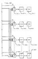
- FIG. 1 there is illustrated one example of an N x M arbitrating non-blocking high bandwidth switch in a multiprocessor system.
- the system shown in Figure 1 refers to processors 11 through 14 being selectively coupled to one of four basic storage modules (BSM) 21 through 24. In actual practice, the number of processors connected to basic storage may be 32 or greater.
- BSM basic storage modules
- the inputs from the processors 11 through 14 are applied to respective buffers 31 through 34. These buffers 31 through 34 may be for example FIFO (First In, First Out) buffers.
- the output from each of the processors 11 through 14 includes a request code signal and associated data signals or data packet.
- the request code signal could be simply a logic 1 level at one of the four lead wires.
- the output request code signal from each of the buffers 31 through 34 is applied to each of four arbitrators 41 through 44.
- the request code signal and associated data signals or data packet are sequenced together through the buffers 31 through 34.
- the request code signal could be via four wires or lines, with only one of the four wires being at a logic 1 level and the other three wires being at a logic zero level.
- the logic 1 level may be five volts where the logic zero may be at ground potential. If, for example, processor 11 wants to be coupled to BSM 21, the processor 11 provides a logic 1 level on lead 101 from buffer 31 and logic 0 level to leads 102 through 104 at the first request ports of arbitrators 42 through 44.
- processor 11 wants to be coupled to BSM 22, BSM 23, or BSM 24, the logic 1 level would only be on line 102, 103, or 104 respectively.
- processor 14 requests to be coupled to BSM 21, BSM 22, BSM 23, or BSM 24, the logic 1 level would only be on line 141, 142, 143, or 144 respectively.
- processors 12 and 13 can be coupled to any one of the basic BSM modules 21 through 24 by appropriate logic 1 level at the request line to arbitrators 41 through 44 respectively.
- Each arbitrator first determines if there is an input from any of the four FIFO buffers 31 through 34. If there is more than one input to that arbitrator, it sequences the data inputs each clock cycle through an associated selector 51 through 54. The data is sent to all four selectors 51 through 54. If there are no contentions or more than one processor trying to use a given storage module at the arbitrator, the input from each buffer 31 through 34 at each selector 51 through 54 is simultaneously coupled to the associated BSM 21 through 24 via associated buffer 61 through 64. Selectors 51 through 54 are associated with each of the BSM 21 through 24.
- the arbitrator 41 through 44 identify which output BSM 21 through 24 the input data from a given processor is to be applied and provide a select code to the selectors 51 through 54 to gate the data from buffers 31 through 34 to the appropriate one of buffers 51 through 64.
- one of the arbitrators 41 through 44 associated with a given BSM determines the sequence out of the associated selectors 51 through 54. For example, if there is a request code signal from processor 11 and from processor 12 via buffers 31 and 32 for BSM 21, they are both applied to the arbitrator 41.
- the arbitrator 41 provides, for example, a first select code to the selector 51 during the first clock pulse to gate the output from the FIFO buffer 31 through the selector 51 to buffer 61 and to the BSM 21.
- the second select signal code is provided to selector 51 and processor 12 data at buffer 32 is coupled through the selector 51 to the BSM Module 21.
- FIG 2 there is illustrated a logic block diagram for each arbitrator of Figure 1.
- the first input port 201 is coupled to processor 11 via buffer 31.
- this input port 201 is coupled via wire lead 101.
- the second input port 202 is coupled to processor 12 via buffer 32, the third port 203 is coupled to processor 13 via buffer 33 and the fourth port 204 is coupled to processor 14 via buffer 34.
- the request at inputs 201 through 204 are applied to the respective AND gates A1 through A4.
- the outputs from AND gates A1 through A4 are applied to the set inputs of flip-flop registers S1 through S4.
- the Q output from register S1 is applied directly to the output lead 205 and to NOR gate 100.
- the Q outputs from the registers S2 through S4 are also applied to the NOR gate 100.
- the Q output of switching register S1 is applied to AND Gate A5.
- the Q output from register S2 is also applied to the AND Gate A5.
- the Q output of switches S3 and S4 are coupled to the respective inputs of AND Gates A6 and A7.
- AND Gate A6 also receives the Q output from registers S1 and S2.
- AND Gate A7 receives a Q output from registers S1, S2 and S3 and the Q output from register S4.
- the Q output from switch S1 is applied to the reset input of switch S1.
- the output of AND Gate A5 is coupled to the reset input of register S2.
- the output of AND Gate A6 coupled to the reset input of register S3 and the output of AND Gate A7 is coupled to the reset input of register S4.
- the outputs of AND Gates A5 through A7 on leads 206 through 208 and the Q output of register S1 on lead 205 provide a four-bit address code which is applied to the corresponding selector 51 through 54 to select the output.
- one of the arbitrator outputs 205 through 208 having a logic 1 level would enable the associated processor data to the associated basic storage module. For example, if the output from register S1 is at the logic 1 level, the processor 11 output will be coupled to the basic storage module associated with the arbitrator.
- processor 11 data would be coupled to BSM 21. If at arbitrator 42 processor 11 data is coupled to BSM 22, if at arbitrator 43 processor 11 data is coupled to BSM 23, and if at arbitrator 44 processor 11 data is coupled to BSM 24. If at arbitrator 41 there is a logic 1 level at output 208 of arbitrator 41, the data from processor 14 would be coupled to the basic storage module 21. If the logic 1 level is at output 208 of arbitrator 42, the data from processor 14 is coupled to BSM 22. If at arbitrator 43 from processor 14 to BSM 23, etc.
- the NOR Gate 100 provides a logic 1 level to AND Gates A1 through A4 with all zeros at its input. If there is only a request or logic 1 level at input 202, for example, this output enables AND Gate A2 with a logic 1 coupled to the set input of switch S2 to thereby provide a logic 1 level at the Q output of register S2.
- the logic 1 level output from register S2 is coupled to the NOR Gate 100 and in response to this logic 1 a logic low or zero level from NOR Gate 100 is provided to AND Gates A1 through A2, stopping all further requests.
- the logic 1 level input at AND Gate A5 from register S2 enables the logic 1 level input from the Q output of register S1 to provide logic 1 level at the output 206.
- This code with a logic 1 level only on lead 206 requests the selector 51 through 54 associated with the arbitrator to couple the data from the second processor 12 to the basic storage module associated with the selector. For example, with arbitrator 41 the data from processor 12 is coupled to BSM 21.
- the arbitrator 41 sees the presence of a logic 1 level at AND Gates A1 and A3 to enable the logic 1 from NOR Gate 100 to produce a set of logic 1 levels at the set inputs of registers S1 and S3. This produces a logic 1 level at the Q outputs of registers S1 and S3.
- the presence of the logic 1 level at either of these "Q" outputs at the NOR Gate 100 provides a logic "0" at the AND Gates A1 through A4 which stops any further requests.
- a logic zero or low level is provided from the Q outputs of registers S1 and S3 to the AND Gates A5 through A7.
- AND Gate A6 output remains at a logic zero with the Q output from register S1 being low.
- the register S1 is reset via lead 209 providing a logic one at the Q output of register S1 to AND gate A6 and allowing the request at input 203 to provide a logic 1 from AND gate A6.
- This logic 1 at output 207 of AND gate A6 selects the data then from processor 13 to the associated BSM on the next clock cycle.
- register S3 is reset by the feedback path 210 from AND gate A6 and the NOR output from NOR Gate 100 goes high.
- the NOR Gate output goes high, all of the registers S1 through S4 are off and any combination of input request can be acknowledged in the next full cycle.
- the arbitrators as shown in Figure 2 always acknowledge multiple requests in round-robin order of S1 through S4 until all are satisfied; that is, in instant case the request at input 201 has the highest priority with request at input 202 second, input at 203 third and input at 204 having the lowest priority within that arbitration cycle.
- each processor 301-332 provides a 5-bit encoded request signal for each data block or packet to be applied to the BSM.
- the request code signal with its associated data packet is sequenced through the associated buffer.
- a decoder 301a-332a is at the output of each input buffer 301b-332b for decoding each 5-bit processor encoded request signal and providing a logic 1 request via lead on one of the 32 output lines to the appropriate arbitrator.
- decoder 301a decodes the encoded output from buffer 301b indicating it's data to be applied to BSM 302f and provides a logic 1 on lead 400 or request to arbitrator 302c.
- the data at buffer 301b is then enabled through select switch 302d to memory BSM 302f via buffer 302e.
- the arbitrators 301c-332c would be like Figure 2 with 32 inputs and outputs instead of four input and outputs.
Applications Claiming Priority (2)
| Application Number | Priority Date | Filing Date | Title |
|---|---|---|---|
| US152779 | 1988-02-05 | ||
| US07/152,779 US4991084A (en) | 1988-02-05 | 1988-02-05 | N×M round robin order arbitrating switching matrix system |
Publications (3)
| Publication Number | Publication Date |
|---|---|
| EP0327203A2 true EP0327203A2 (fr) | 1989-08-09 |
| EP0327203A3 EP0327203A3 (fr) | 1991-05-02 |
| EP0327203B1 EP0327203B1 (fr) | 1995-10-04 |
Family
ID=22544410
Family Applications (1)
| Application Number | Title | Priority Date | Filing Date |
|---|---|---|---|
| EP89300139A Expired - Lifetime EP0327203B1 (fr) | 1988-02-05 | 1989-01-09 | Commutateur NxM d'arbitrage sans blocage à grande bande passante |
Country Status (4)
| Country | Link |
|---|---|
| US (1) | US4991084A (fr) |
| EP (1) | EP0327203B1 (fr) |
| JP (1) | JPH0766363B2 (fr) |
| DE (1) | DE68924435T2 (fr) |
Cited By (5)
| Publication number | Priority date | Publication date | Assignee | Title |
|---|---|---|---|---|
| EP0597013A1 (fr) * | 1991-07-26 | 1994-05-18 | Tandem Computers Incorporated | Appareil et procede de commutation de blocs de donnees |
| WO1998052126A1 (fr) * | 1997-05-16 | 1998-11-19 | Unisys Corporation | Regisseur de memoire a echelle modulable |
| EP1058890A1 (fr) * | 1998-02-03 | 2000-12-13 | SRC Computers Inc. | Systeme et procede de resolution dynamique de conflits de priorite dans un systeme informatique multiprocesseur comportant des ressources de memoire partagees |
| WO2003017116A1 (fr) * | 2001-08-13 | 2003-02-27 | Inrange Technologies Corporation | Circuit d'arbitrage multiple dans une matrice de commutation de points de connexion |
| WO2006071942A2 (fr) * | 2004-12-28 | 2006-07-06 | Intel Corporation | Procede et appareil de mise en oeuvre d'interconnexions heterogenes |
Families Citing this family (16)
| Publication number | Priority date | Publication date | Assignee | Title |
|---|---|---|---|---|
| DE68929288T2 (de) * | 1988-12-19 | 2001-11-15 | Nec Corp | Datenübertragungsvorrichtung |
| EP0429733B1 (fr) * | 1989-11-17 | 1999-04-28 | Texas Instruments Incorporated | Multiprocesseur avec commutateur à coordonnées entre processeurs et mémoires |
| KR940001878B1 (ko) * | 1990-03-08 | 1994-03-10 | 가부시끼가이샤 히다찌세이사꾸쇼 | 멀티 프로세서시스템 및 인터럽션 제어장치 |
| US6928500B1 (en) * | 1990-06-29 | 2005-08-09 | Hewlett-Packard Development Company, L.P. | High speed bus system that incorporates uni-directional point-to-point buses |
| US5276808A (en) * | 1991-02-04 | 1994-01-04 | International Business Machines Corporation | Data storage buffer system and method |
| US5371893A (en) * | 1991-12-27 | 1994-12-06 | International Business Machines Corporation | Look-ahead priority arbitration system and method |
| US5274785A (en) * | 1992-01-15 | 1993-12-28 | Alcatel Network Systems, Inc. | Round robin arbiter circuit apparatus |
| US5301332A (en) * | 1992-12-23 | 1994-04-05 | Ncr Corporation | Method and apparatus for a dynamic, timed-loop arbitration |
| US5506968A (en) * | 1992-12-28 | 1996-04-09 | At&T Global Information Solutions Company | Terminating access of an agent to a shared resource when a timer, started after a low latency agent requests access, reaches a predetermined value |
| JPH07105175A (ja) * | 1993-10-08 | 1995-04-21 | Nec Corp | マイクロコンピュータ |
| CA2145553C (fr) * | 1994-03-30 | 1999-12-21 | Yuuki Date | Systeme multiprocesseur comportant un arbitre de priorite pour les demandes des processeurs |
| JPH0981508A (ja) * | 1995-08-31 | 1997-03-28 | Internatl Business Mach Corp <Ibm> | 通信方法及び装置 |
| US6272580B1 (en) | 1999-03-16 | 2001-08-07 | Compaq Computer Corp. | Apparatus and method for dynamically elevating a lower level bus master to an upper level bus master within a multi-level arbitration system |
| US7284082B2 (en) * | 2004-08-19 | 2007-10-16 | Lsi Corporation | Controller apparatus and method for improved data transfer |
| US20070124554A1 (en) * | 2005-10-28 | 2007-05-31 | Honeywell International Inc. | Global memory for a rapidio network |
| US11520713B2 (en) * | 2018-08-03 | 2022-12-06 | International Business Machines Corporation | Distributed bus arbiter for one-cycle channel selection using inter-channel ordering constraints in a disaggregated memory system |
Citations (3)
| Publication number | Priority date | Publication date | Assignee | Title |
|---|---|---|---|---|
| US3096447A (en) * | 1961-03-21 | 1963-07-02 | Gen Precision Inc | Transistor gate biased by signal being gated |
| GB1170434A (en) * | 1965-11-16 | 1969-11-12 | Gen Electric | Data Processing System |
| EP0097351A2 (fr) * | 1982-06-21 | 1984-01-04 | Nec Corporation | Unité d'acheminement et réseau d'acheminement pour la détermination d'une porte de sortie par la détection d'une partie d'un paquet d'entrée |
Family Cites Families (13)
| Publication number | Priority date | Publication date | Assignee | Title |
|---|---|---|---|---|
| JPS5917595B2 (ja) * | 1979-11-29 | 1984-04-21 | 岩崎通信機株式会社 | 通話路スイツチ回路網 |
| NL8000529A (nl) * | 1980-01-29 | 1981-08-17 | Philips Nv | Schakelmatrix. |
| US4314335A (en) * | 1980-02-06 | 1982-02-02 | The Perkin-Elmer Corporation | Multilevel priority arbiter |
| US4417245A (en) * | 1981-09-02 | 1983-11-22 | International Business Machines Corp. | Digital space division exchange |
| FR2513407B1 (fr) * | 1981-09-24 | 1987-01-16 | Finger Ulrich | Systeme d'arbitrage des demandes d'acces de plusieurs processeurs a des ressources communes, par l'intermediaire d'un bus commun |
| US4488218A (en) * | 1982-01-07 | 1984-12-11 | At&T Bell Laboratories | Dynamic priority queue occupancy scheme for access to a demand-shared bus |
| US4473880A (en) * | 1982-01-26 | 1984-09-25 | Intel Corporation | Arbitration means for controlling access to a bus shared by a number of modules |
| JPS6054694B2 (ja) * | 1982-01-27 | 1985-12-02 | 株式会社日立製作所 | 記憶制御装置 |
| JPS59111891A (ja) * | 1982-12-16 | 1984-06-28 | Ricoh Co Ltd | 感熱転写媒体 |
| JPS59161755A (ja) * | 1983-03-07 | 1984-09-12 | Hitachi Ltd | 記憶制御方式 |
| US4706150A (en) * | 1984-06-29 | 1987-11-10 | International Business Machines Corporation | Switching protocal for multiple autonomous switching planes |
| JPH0628051B2 (ja) * | 1986-04-25 | 1994-04-13 | 株式会社日立製作所 | 記憶制御方式 |
| US4807184A (en) * | 1986-08-11 | 1989-02-21 | Ltv Aerospace | Modular multiple processor architecture using distributed cross-point switch |
-
1988
- 1988-02-05 US US07/152,779 patent/US4991084A/en not_active Expired - Fee Related
- 1988-11-17 JP JP63289036A patent/JPH0766363B2/ja not_active Expired - Lifetime
-
1989
- 1989-01-09 DE DE68924435T patent/DE68924435T2/de not_active Expired - Fee Related
- 1989-01-09 EP EP89300139A patent/EP0327203B1/fr not_active Expired - Lifetime
Patent Citations (3)
| Publication number | Priority date | Publication date | Assignee | Title |
|---|---|---|---|---|
| US3096447A (en) * | 1961-03-21 | 1963-07-02 | Gen Precision Inc | Transistor gate biased by signal being gated |
| GB1170434A (en) * | 1965-11-16 | 1969-11-12 | Gen Electric | Data Processing System |
| EP0097351A2 (fr) * | 1982-06-21 | 1984-01-04 | Nec Corporation | Unité d'acheminement et réseau d'acheminement pour la détermination d'une porte de sortie par la détection d'une partie d'un paquet d'entrée |
Non-Patent Citations (1)
| Title |
|---|
| IEEE TRANSACTIONS ON COMPUTERS. vol. C-34, no. 10, October 1985, NEW YORK US pages 918 - 926; C.R.DAS et al: "Bandwidth Availability of Multiple-Bus Multiprocessors" * |
Cited By (13)
| Publication number | Priority date | Publication date | Assignee | Title |
|---|---|---|---|---|
| EP0597013A4 (en) * | 1991-07-26 | 1994-08-10 | Tandem Computers Inc | Apparatus and method for frame switching. |
| US5455917A (en) * | 1991-07-26 | 1995-10-03 | Tandem Computers Incorporated | Apparatus and method for frame switching |
| EP0597013A1 (fr) * | 1991-07-26 | 1994-05-18 | Tandem Computers Incorporated | Appareil et procede de commutation de blocs de donnees |
| WO1998052126A1 (fr) * | 1997-05-16 | 1998-11-19 | Unisys Corporation | Regisseur de memoire a echelle modulable |
| US6006296A (en) * | 1997-05-16 | 1999-12-21 | Unisys Corporation | Scalable memory controller |
| EP1058890A4 (fr) * | 1998-02-03 | 2004-06-23 | Src Computers Inc | Systeme et procede de resolution dynamique de conflits de priorite dans un systeme informatique multiprocesseur comportant des ressources de memoire partagees |
| EP1058890A1 (fr) * | 1998-02-03 | 2000-12-13 | SRC Computers Inc. | Systeme et procede de resolution dynamique de conflits de priorite dans un systeme informatique multiprocesseur comportant des ressources de memoire partagees |
| WO2003017116A1 (fr) * | 2001-08-13 | 2003-02-27 | Inrange Technologies Corporation | Circuit d'arbitrage multiple dans une matrice de commutation de points de connexion |
| WO2006071942A2 (fr) * | 2004-12-28 | 2006-07-06 | Intel Corporation | Procede et appareil de mise en oeuvre d'interconnexions heterogenes |
| WO2006071942A3 (fr) * | 2004-12-28 | 2006-08-24 | Intel Corp | Procede et appareil de mise en oeuvre d'interconnexions heterogenes |
| US7353317B2 (en) | 2004-12-28 | 2008-04-01 | Intel Corporation | Method and apparatus for implementing heterogeneous interconnects |
| US7640387B2 (en) | 2004-12-28 | 2009-12-29 | Intel Corporation | Method and apparatus for implementing heterogeneous interconnects |
| DE112005003274B4 (de) * | 2004-12-28 | 2013-09-12 | Intel Corporation | Verfahren und Vorrichtung zur Implementierung heterogener Verbindungen |
Also Published As
| Publication number | Publication date |
|---|---|
| EP0327203A3 (fr) | 1991-05-02 |
| US4991084A (en) | 1991-02-05 |
| JPH01206450A (ja) | 1989-08-18 |
| DE68924435T2 (de) | 1996-05-30 |
| EP0327203B1 (fr) | 1995-10-04 |
| DE68924435D1 (de) | 1995-11-09 |
| JPH0766363B2 (ja) | 1995-07-19 |
Similar Documents
| Publication | Publication Date | Title |
|---|---|---|
| EP0327203B1 (fr) | Commutateur NxM d'arbitrage sans blocage à grande bande passante | |
| US4577273A (en) | Multiple microcomputer system for digital computers | |
| US4152764A (en) | Floating-priority storage control for processors in a multi-processor system | |
| US5371893A (en) | Look-ahead priority arbitration system and method | |
| US5426612A (en) | First-in first-out semiconductor memory device | |
| US5237567A (en) | Processor communication bus | |
| US4451881A (en) | Data processing system bus for multiple independent users | |
| US3766526A (en) | Multi-microprogrammed input-output processor | |
| US5168570A (en) | Method and apparatus for a multiple request toggling priority system | |
| US3447135A (en) | Peripheral data exchange | |
| EP0383475A2 (fr) | Arbitrage de ressources partagées | |
| US4744023A (en) | Processor access control arrangement in a multiprocessor system | |
| US5515523A (en) | Method and apparatus for arbitrating conflicts by monitoring number of access requests per unit of time in multiport memory systems | |
| US4115854A (en) | Channel bus controller | |
| US4835672A (en) | Access lock apparatus for use with a high performance storage unit of a digital data processing system | |
| EP0550147A1 (fr) | Méthode et appareil d'arbitrage basés sur la disponibilité des ressources | |
| US4905145A (en) | Multiprocessor | |
| EP0051426A1 (fr) | Mise en file d'attente de demandes dans une unité de commande de mémoire | |
| US6628662B1 (en) | Method and system for multilevel arbitration in a non-blocking crossbar switch | |
| US5828891A (en) | Multilevel interrupt device | |
| EP0865633B1 (fr) | Processeur de donnees a semi-conducteurs dote d'un systeme d'interruption multisource polyvalent | |
| US4648065A (en) | Modified snapshot priority enabling two requestors to share a single memory port | |
| US5692136A (en) | Multi-processor system including priority arbitrator for arbitrating request issued from processors | |
| US5440689A (en) | Interprocessor communication system for direct processor to processor communication between internal general purpose registers transparent to the execution of processors thereof | |
| EP0118670A2 (fr) | Système de priorité pour sous-système de canal |
Legal Events
| Date | Code | Title | Description |
|---|---|---|---|
| PUAI | Public reference made under article 153(3) epc to a published international application that has entered the european phase |
Free format text: ORIGINAL CODE: 0009012 |
|
| AK | Designated contracting states |
Kind code of ref document: A2 Designated state(s): DE FR GB |
|
| 17P | Request for examination filed |
Effective date: 19891214 |
|
| PUAL | Search report despatched |
Free format text: ORIGINAL CODE: 0009013 |
|
| AK | Designated contracting states |
Kind code of ref document: A3 Designated state(s): DE FR GB |
|
| 17Q | First examination report despatched |
Effective date: 19940113 |
|
| GRAA | (expected) grant |
Free format text: ORIGINAL CODE: 0009210 |
|
| AK | Designated contracting states |
Kind code of ref document: B1 Designated state(s): DE FR GB |
|
| PG25 | Lapsed in a contracting state [announced via postgrant information from national office to epo] |
Ref country code: FR Effective date: 19951004 |
|
| REF | Corresponds to: |
Ref document number: 68924435 Country of ref document: DE Date of ref document: 19951109 |
|
| EN | Fr: translation not filed | ||
| PLBE | No opposition filed within time limit |
Free format text: ORIGINAL CODE: 0009261 |
|
| STAA | Information on the status of an ep patent application or granted ep patent |
Free format text: STATUS: NO OPPOSITION FILED WITHIN TIME LIMIT |
|
| 26N | No opposition filed | ||
| PGFP | Annual fee paid to national office [announced via postgrant information from national office to epo] |
Ref country code: GB Payment date: 19961220 Year of fee payment: 9 |
|
| PGFP | Annual fee paid to national office [announced via postgrant information from national office to epo] |
Ref country code: DE Payment date: 19970128 Year of fee payment: 9 |
|
| PG25 | Lapsed in a contracting state [announced via postgrant information from national office to epo] |
Ref country code: GB Free format text: LAPSE BECAUSE OF NON-PAYMENT OF DUE FEES Effective date: 19980109 |
|
| GBPC | Gb: european patent ceased through non-payment of renewal fee |
Effective date: 19980109 |
|
| PG25 | Lapsed in a contracting state [announced via postgrant information from national office to epo] |
Ref country code: DE Free format text: LAPSE BECAUSE OF NON-PAYMENT OF DUE FEES Effective date: 19981001 |