EP0326006A2 - Circuit de conversion de format pour des données numériques - Google Patents
Circuit de conversion de format pour des données numériques Download PDFInfo
- Publication number
- EP0326006A2 EP0326006A2 EP89100792A EP89100792A EP0326006A2 EP 0326006 A2 EP0326006 A2 EP 0326006A2 EP 89100792 A EP89100792 A EP 89100792A EP 89100792 A EP89100792 A EP 89100792A EP 0326006 A2 EP0326006 A2 EP 0326006A2
- Authority
- EP
- European Patent Office
- Prior art keywords
- unsigned
- signed
- input
- numeric data
- data
- Prior art date
- Legal status (The legal status is an assumption and is not a legal conclusion. Google has not performed a legal analysis and makes no representation as to the accuracy of the status listed.)
- Granted
Links
Images


Classifications
-
- G—PHYSICS
- G06—COMPUTING; CALCULATING OR COUNTING
- G06F—ELECTRIC DIGITAL DATA PROCESSING
- G06F7/00—Methods or arrangements for processing data by operating upon the order or content of the data handled
-
- G—PHYSICS
- G06—COMPUTING; CALCULATING OR COUNTING
- G06F—ELECTRIC DIGITAL DATA PROCESSING
- G06F7/00—Methods or arrangements for processing data by operating upon the order or content of the data handled
- G06F7/38—Methods or arrangements for performing computations using exclusively denominational number representation, e.g. using binary, ternary, decimal representation
- G06F7/48—Methods or arrangements for performing computations using exclusively denominational number representation, e.g. using binary, ternary, decimal representation using non-contact-making devices, e.g. tube, solid state device; using unspecified devices
- G06F7/52—Multiplying; Dividing
- G06F7/535—Dividing only
-
- G—PHYSICS
- G06—COMPUTING; CALCULATING OR COUNTING
- G06F—ELECTRIC DIGITAL DATA PROCESSING
- G06F5/00—Methods or arrangements for data conversion without changing the order or content of the data handled
-
- G—PHYSICS
- G06—COMPUTING; CALCULATING OR COUNTING
- G06F—ELECTRIC DIGITAL DATA PROCESSING
- G06F9/00—Arrangements for program control, e.g. control units
- G06F9/06—Arrangements for program control, e.g. control units using stored programs, i.e. using an internal store of processing equipment to receive or retain programs
- G06F9/30—Arrangements for executing machine instructions, e.g. instruction decode
- G06F9/30003—Arrangements for executing specific machine instructions
- G06F9/30007—Arrangements for executing specific machine instructions to perform operations on data operands
- G06F9/30025—Format conversion instructions, e.g. Floating-Point to Integer, decimal conversion
Definitions
- the present invention relates to a logic circuit for converting the format of numeric data, and particularly to a format converting circuit for converting unsigned numeric data into signed numeric data and signed numeric data into unsigned numeric data.
- the multiplication or the division of signed numbers (the most significant bit of each of the signed numbers represents a sign, and a negative number is represented with a two's complement of the number) is carried out by converting the signed numbers into unsigned numbers (absolute values). An unsigned result of the multiplication or the division is converted into a signed number according to a decision rule.
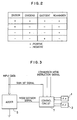
- Fig. 1 shows an example of the conversion. If a multiplier and a multiplicand in a multiplication operation have the same sign, the sign of a product of the multiplication will be positive and, if they have different signs, it will be negative. Therefore, in converting an unsigned product into a signed number, it is necessary only to see whether or not a multiplier and a multiplicand have the same sign.
- the signs of a quotient and a remainder in a division operation are determined according to separate rules as shown in Fig. 2. Therefore, in converting an unsigned quotient and an unsigned remainder into signed numbers, it is necessary to see not only whether or not the signs of a divisor and a dividend are the same but also what the sign of the dividend is.
- a conventional converting circuit shown in Fig. 3 uses two flip-flop circuits 1 and 3 for storing the signs of numeric data shown in Fig. 2.
- a conversion mode instruction signal is given to a control circuit 7 to specify a signed-to-unsigned conversion mode.
- a sign bit of the signed number is 0, an adder 5 outputs the number as it is while, if the sign bit is 1, the adder 5 calculates and outputs a two's complement of the number.
- the sign bits of numeric data are stored in the flip-flops 1 or 3, according to the conversion mode instruction signal.
- the conversion mode instruction signal instructs the control circuit 7 an unsigned-to-signed conversion mode as well as informing the control circuit 7 of whether the unsigned operation result is a quotient (or a product) or a remainder.
- an exclusive OR of sign bits stored in the flip-flops 1 and 3 determines an operation mode of the adder 5. Namely, if the exclusive OR is 0, the adder 5 outputs the quotient (or the product) as it is and, if it is 1, the adder 5 outputs a two's complement of the quotient (or the product).
- a sign bit (indicating the sign of a dividend) stored in the flip-flop 3 determines an operation mode of the adder 5. If the sign bit is 0, the adder 5 outputs the remainder as it is and, if it is 1, the adder 5 outputs a two's complement of the remainder.
- the conventional converting circuit stores the signs of two numeric data separately, and uses them to determine the sign of an operation result. Due to this, the conventional circuit has drawbacks mentioned below.
- Two flip-flops shall be arranged to store the sign bits of two input data, respectively.
- An object of the present invention is to provide a format converting circuit for numeric data, having a simple constitution compared to that of a conventional circuit.
- the present invention provides a format converting circuit for numeric data, comprising an operation means which operates according to a mode decision signal to output an input data as it is or a two's complement of the input data; a storage means which stores a positive or negative sign data to be read out and is reset by an initializing signal to a positive sign data possessing state; and a control means which operates in two conversion modes.
- One of the modes is a signed-to-unsigned conversion mode in which the control means sends the mode decision signal to the operation means to control it such that, if the sign bit of an input numeric data to the operation means is 0, the operation means passes the numeric data as it is while, if the sign bit is 1, the operation means calculates and outputs a two's complement of the numeric data.
- the control means inverts a value in the storage means, if the above-mentioned sign bit is 1.
- the other mode is an unsigned-to-signed conversion mode in which the control means sends the mode decision signal to the operation means to control it such that, if the value stored in the storage means is positive, the operation means outputs in inputted data as it is while, if the value stored in the storage means is negative, the operation means outputs a two's complement of the inputted data.
- control means To convert a signed multiplier and multiplicand or divisor and dividend into unsigned numbers, the control means is set to the signed-to-unsigned conversion mode before inputting the numeric data.
- control means To convert an unsigned quotient or an unsigned product into a signed number, the control means is set to the unsigned-to-signed conversion mode before inputting the quotient or the product.
- control means To convert an unsigned remainder into a signed number, the control means is firstly set to the signed-to-unsigned conversion mode to input a divisor. Then, the control means is set to the unsigned-to-signed conversion mode to input the remainder.
- a positive sign data is stored in the storage means if an exclusive OR of the sign bits of two numeric data is 0 (i.e., the sign bits are equal to each other), while a negative sign data is stored in the storage means if the exclusive OR of the sign bits is 1 (i.e., the sign bits are different from each other). Therefore, only one flip-flop for storing the sign bits is needed.
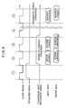
- Fig. 4 is a view showing a format converting circuit of numeric data according to an embodiment of the present invention.
- the format converting circuit has an adder 9.
- the adder 9 operates according to a mode decision signal from a control circuit 13 to output an input number as it is (a through mode) or to output a two's complement of the input number (a complement mode).
- a flip-flop 11 stores a sign data from the control circuit 13, and latches an input signal in synchronism with a clock signal.
- the flip-flop circuit 11 is reset to 0 by an initializing signal.
- the control circuit 13 is put, according to a conversion mode instruction signal, in a signed-to-unsigned conversion mode or to an unsigned-to-signed conversion mode.
- the control circuit 13 puts the adder 9 in the through mode if the sign bit of a numeric data inputted to the adder 9 is 0, and puts the adder 9 in the complement mode if the sign bit is 1.
- the control circuit 13 finds an exclusive OR of the sign bit of the input data with respect to a sign data stored in the flip-flop 11, and transfers the exclusive OR to the flip-flop 11. Therefore, if the sign of the input data is 0, the value of the flip-flop 11 will not be changed and, if the sign bit of the input data is 1, the value of the flip-flop 11 will be inverted.
- the control circuit 13 puts the adder 9 in the through mode to pass an input numeric data as it is if a value stored in the flip-flop 11 is 0, and puts the adder 9 in the complement mode to output a tow's complement of the input data if the value of the flip-flop 11 is 1.
- Fig. 5 is a timing chart in finding a quotient of division
- Fig. 7 shows values to be stored in the flip-flop 11 at respective cycles of the converting operation.
- an initializing signal is set to HIGH to reset the flip-flop 11 to 0 as shown in a column 1 of the table of Fig. 7.
- a conversion mode instruction signal specifying the signed-to-unsigned conversion mode is sent to the control circuit 13, and a numeric data of divisor is inputted to the adder 9.
- the input numeric data is outputted as it is from the adder 9 if a sign bit of the inputted data is 0, and a two's complement of the inputted numeric data is outputted from the adder 9 if the sign bit is 1.
- the sign bit is 0, a status of the flip-flop 11 will not be changed while, if the sign bit is 1, the status of the flip-flop 11 will be inverted. Namely, as shown in a column 2 of the table of Fig. 7, the flip-flop 11 will be 1 if the sign bit of the divisor is negative.
- a dividend is inputted. Similar to the case of the divisor, the inputted number is outputted as it is if a sign bit of the inputted number is 0, and a two's complement of the inputted number is outputted if the sign bit is 1. Further, if the sign bit is 0, the status of the flip-flop 11 will not be changed while, if the sign bit is 1, the status of the flip-flop 11 will be inverted. As a result, as shown in a column 3 of Fig. 7, the flip-flop 11 will be 0 if the divisor and dividend have the same sign, and the flip-flop 11 will be 1 if the divisor and dividend have different signs, respectively. Namely, an exclusive OR of the sign bits of the divisor and dividend is stored in the flip-flop 11.
- the conversion mode instruction signal is set to LOW in the next clock cycle 4 to put the converting circuit in the unsigned-to-signed conversion mode. During this clock cycle, a division operation is executed according to the unsigned divisor and dividend.
- an unsigned quotient is inputted in the next cycle 5.
- the inputted quotient is outputted as it is if the status of the flip-flop 11 is 0, while a two's complement of the inputted quotient is outputted if the status of the flip-flop 11 is 1, thus converting the quotient into a signed number.
- the converting circuit is put in the signed-to-unsigned conversion mode in a clock cycle 5 shown in Fig. 6, and a signed divisor is inputted for a second time. If the sign bit of the divisor is 0, a value stored in the flip-flop 11 will not be changed while, if the sign bit is 1, the value in the flip-flop 11 will be inverted. As a result, as shown in a column 5 of Fig. 7, the value of the flip-flop 11 will be equal to a value of the sign bit of a dividend. According to the value of the sign bit, the divisor is outputted as it is, or a two's complement of the divisor data is outputted. However, the outputted data is ignored.
- the converting circuit is put in the unsigned-to-signed conversion mode, and an unsigned remainder is inputted. Similar to the case of the quotient, the inputted remainder is outputted as it is if the value of the flip-flop 11 is 0 and, if the flip-flop is 1, a two's complement of the remainder is outputted.
- both the quotient and remainder can be found by continuously executing the conversion operation on the quotient and remainder to consecutively convert the unsigned quotient and remainder into signed numbers.
- a conversion operation related to multiplication can be executed in a manner similar to that of finding a quotient of division.
- an adder has been used to output an input signal of n bits as it is, or to output a two's complement of the input signal.
- This adder may be replaced with another device, if the device has the same function as that of the adder.
- a standard arithmetic logic operation unit ALU which executes arithmetic and logic operation with respect to a plurality of input data may be used.
- the control circuit 13 may be controlled with a microprogram such that the conversion mode instruction signal is given to the control circuit 13 as a code of an operation field of a microinstruction, as shown in Fig. 10.
- the code of the operation field will be satisfactory if it can specify the two converting operations, i.e., the signed-to-unsigned and unsigned-to-signed conversion operations so that the operation field code is needed to have only one bit.
Applications Claiming Priority (2)
| Application Number | Priority Date | Filing Date | Title |
|---|---|---|---|
| JP7034/88 | 1988-01-18 | ||
| JP63007034A JPH0774989B2 (ja) | 1988-01-18 | 1988-01-18 | 符号変換回路 |
Publications (3)
| Publication Number | Publication Date |
|---|---|
| EP0326006A2 true EP0326006A2 (fr) | 1989-08-02 |
| EP0326006A3 EP0326006A3 (fr) | 1991-07-03 |
| EP0326006B1 EP0326006B1 (fr) | 1995-06-21 |
Family
ID=11654754
Family Applications (1)
| Application Number | Title | Priority Date | Filing Date |
|---|---|---|---|
| EP89100792A Expired - Lifetime EP0326006B1 (fr) | 1988-01-18 | 1989-01-18 | Circuit de conversion de format pour des données numériques |
Country Status (5)
| Country | Link |
|---|---|
| US (1) | US4935890A (fr) |
| EP (1) | EP0326006B1 (fr) |
| JP (1) | JPH0774989B2 (fr) |
| KR (1) | KR920002572B1 (fr) |
| DE (1) | DE68923100T2 (fr) |
Families Citing this family (8)
| Publication number | Priority date | Publication date | Assignee | Title |
|---|---|---|---|---|
| US5268858A (en) * | 1991-08-30 | 1993-12-07 | Cyrix Corporation | Method and apparatus for negating an operand |
| US5493581A (en) * | 1992-08-14 | 1996-02-20 | Harris Corporation | Digital down converter and method |
| DE69720922T2 (de) | 1996-11-29 | 2003-11-13 | Matsushita Electric Ind Co Ltd | Prozessor mit verbessertem Rundungsprozess |
| US6085207A (en) * | 1997-06-12 | 2000-07-04 | Sun Microsystems, Inc. | Method of performing signed operations with unsigned instructions in a microprocessor |
| US6018751A (en) * | 1997-06-13 | 2000-01-25 | Sun Microsystems, Inc. | Microprocessor for performing signed operations with unsigned instructions |
| US6018752A (en) * | 1997-06-16 | 2000-01-25 | Sun Microsystems, Inc. | Microprocessor for performing unsigned operations with signed instructions |
| US6029184A (en) * | 1997-06-17 | 2000-02-22 | Sun Microsystems, Inc. | Method of performing unsigned operations with signed instructions in a microprocessor |
| ITMI20032591A1 (it) * | 2003-12-23 | 2005-06-24 | St Microelectronics Srl | Metodo di rappresentazione codificata di dati e relativo processore di elaborazione dati con circuito di codifica-decodifica |
Citations (1)
| Publication number | Priority date | Publication date | Assignee | Title |
|---|---|---|---|---|
| JPS61201330A (ja) * | 1985-03-05 | 1986-09-06 | Nec Corp | 除算装置 |
Family Cites Families (6)
| Publication number | Priority date | Publication date | Assignee | Title |
|---|---|---|---|---|
| JPS53667B2 (fr) * | 1971-10-23 | 1978-01-11 | ||
| US3786490A (en) * | 1972-04-20 | 1974-01-15 | Bell Telephone Labor Inc | Reversible 2{40 s complement to sign-magnitude converter |
| US4038538A (en) * | 1975-08-18 | 1977-07-26 | Burroughs Corporation | Integer and floating point to binary converter |
| US4520347A (en) * | 1982-11-22 | 1985-05-28 | Motorola, Inc. | Code conversion circuit |
| DE3335386A1 (de) * | 1983-09-29 | 1985-04-11 | Siemens AG, 1000 Berlin und 8000 München | Schaltung zur csd-codierung einer im zweierkomplement dargestellten, binaeren zahl |
| US4709226A (en) * | 1985-07-15 | 1987-11-24 | Rca Corporation | Circuitry for complementing binary numbers |
-
1988
- 1988-01-18 JP JP63007034A patent/JPH0774989B2/ja not_active Expired - Fee Related
-
1989
- 1989-01-03 US US07/293,128 patent/US4935890A/en not_active Expired - Lifetime
- 1989-01-18 EP EP89100792A patent/EP0326006B1/fr not_active Expired - Lifetime
- 1989-01-18 DE DE68923100T patent/DE68923100T2/de not_active Expired - Fee Related
- 1989-01-18 KR KR1019890000481A patent/KR920002572B1/ko not_active IP Right Cessation
Patent Citations (1)
| Publication number | Priority date | Publication date | Assignee | Title |
|---|---|---|---|---|
| JPS61201330A (ja) * | 1985-03-05 | 1986-09-06 | Nec Corp | 除算装置 |
Non-Patent Citations (2)
| Title |
|---|
| COMPUTER DESIGN, vol. 11, no. 5, May 1972, pages 115-121; S. SKLAR: "2's complement arithmetic operations" * |
| PATENT ABSTRACTS OF JAPAN, vol. 11, no. 32 (P-541), 6th September 1986; & JP-A-61 201 330 (NEC) 06-09-1986 * |
Also Published As
| Publication number | Publication date |
|---|---|
| JPH0774989B2 (ja) | 1995-08-09 |
| US4935890A (en) | 1990-06-19 |
| EP0326006B1 (fr) | 1995-06-21 |
| DE68923100T2 (de) | 1995-11-30 |
| KR890012220A (ko) | 1989-08-25 |
| JPH01183733A (ja) | 1989-07-21 |
| KR920002572B1 (ko) | 1992-03-30 |
| EP0326006A3 (fr) | 1991-07-03 |
| DE68923100D1 (de) | 1995-07-27 |
Similar Documents
| Publication | Publication Date | Title |
|---|---|---|
| US4893268A (en) | Circuit and method for accumulating partial products of a single, double or mixed precision multiplication | |
| US4941120A (en) | Floating point normalization and rounding prediction circuit | |
| US5469377A (en) | Floating point computing device for simplifying procedures accompanying addition or subtraction by detecting whether all of the bits of the digits of the mantissa are 0 or 1 | |
| EP0136656A2 (fr) | Mémoire adressable par mi-octet et par mot pour l'accès d'unités de données consécutives pour supporter des opérations arithmétiques décimales | |
| KR860001433B1 (ko) | Rom을 사용하여 10진 승산을 수행하는 데이터 프로세서 | |
| JPH0816365A (ja) | 乗算装置 | |
| US5309383A (en) | Floating-point division circuit | |
| EP0530372A1 (fr) | Convertisseur d'expression numerique et processeur vectoriel l'utilisant | |
| US4302816A (en) | Key input control apparatus | |
| US4617641A (en) | Operation unit for floating point data having a variable length exponent part | |
| US4935890A (en) | Format converting circuit for numeric data | |
| US5247471A (en) | Radix aligner for floating point addition and subtraction | |
| US5195052A (en) | Circuit and method for performing integer power operations | |
| JP3146308B2 (ja) | マトリツクス演算回路 | |
| US6167420A (en) | Multiplication method and multiplication circuit | |
| US4866651A (en) | Method and circuit arrangement for adding floating point numbers | |
| EP0140158B1 (fr) | Dispositif et méthode pour la conversion d'un nombre binaire en un nombre sous un format décimal | |
| US4609997A (en) | Input processor | |
| US4025773A (en) | Enhanced apparatus for binary quotient, binary product, binary sum and binary difference generation | |
| US4928238A (en) | Scalar data arithmetic control system for vector arithmetic processor | |
| US3657529A (en) | Entry mark system for entry and display of numbers | |
| US4644489A (en) | Multi-format binary coded decimal processor with selective output formatting | |
| US4685077A (en) | Data processing apparatus having binary multiplication capability | |
| EP0356940B1 (fr) | Machine à nombre fini d'états | |
| US6792442B1 (en) | Signal processor and product-sum operating device for use therein with rounding function |
Legal Events
| Date | Code | Title | Description |
|---|---|---|---|
| PUAI | Public reference made under article 153(3) epc to a published international application that has entered the european phase |
Free format text: ORIGINAL CODE: 0009012 |
|
| 17P | Request for examination filed |
Effective date: 19890118 |
|
| AK | Designated contracting states |
Kind code of ref document: A2 Designated state(s): DE FR GB |
|
| PUAL | Search report despatched |
Free format text: ORIGINAL CODE: 0009013 |
|
| AK | Designated contracting states |
Kind code of ref document: A3 Designated state(s): DE FR GB |
|
| 17Q | First examination report despatched |
Effective date: 19940329 |
|
| GRAA | (expected) grant |
Free format text: ORIGINAL CODE: 0009210 |
|
| AK | Designated contracting states |
Kind code of ref document: B1 Designated state(s): DE FR GB |
|
| REF | Corresponds to: |
Ref document number: 68923100 Country of ref document: DE Date of ref document: 19950727 |
|
| ET | Fr: translation filed | ||
| PLBE | No opposition filed within time limit |
Free format text: ORIGINAL CODE: 0009261 |
|
| STAA | Information on the status of an ep patent application or granted ep patent |
Free format text: STATUS: NO OPPOSITION FILED WITHIN TIME LIMIT |
|
| 26N | No opposition filed | ||
| PGFP | Annual fee paid to national office [announced via postgrant information from national office to epo] |
Ref country code: FR Payment date: 19980109 Year of fee payment: 10 |
|
| PGFP | Annual fee paid to national office [announced via postgrant information from national office to epo] |
Ref country code: DE Payment date: 19980123 Year of fee payment: 10 |
|
| REG | Reference to a national code |
Ref country code: GB Ref legal event code: 746 Effective date: 19981002 |
|
| PG25 | Lapsed in a contracting state [announced via postgrant information from national office to epo] |
Ref country code: FR Free format text: LAPSE BECAUSE OF NON-PAYMENT OF DUE FEES Effective date: 19990930 |
|
| PG25 | Lapsed in a contracting state [announced via postgrant information from national office to epo] |
Ref country code: DE Free format text: LAPSE BECAUSE OF NON-PAYMENT OF DUE FEES Effective date: 19991103 |
|
| REG | Reference to a national code |
Ref country code: FR Ref legal event code: ST |
|
| REG | Reference to a national code |
Ref country code: GB Ref legal event code: IF02 |
|
| PGFP | Annual fee paid to national office [announced via postgrant information from national office to epo] |
Ref country code: GB Payment date: 20060118 Year of fee payment: 18 |
|
| GBPC | Gb: european patent ceased through non-payment of renewal fee |
Effective date: 20070118 |
|
| PG25 | Lapsed in a contracting state [announced via postgrant information from national office to epo] |
Ref country code: GB Free format text: LAPSE BECAUSE OF NON-PAYMENT OF DUE FEES Effective date: 20070118 |