EP0324205B1 - Amplifier circuit arrangement - Google Patents
Amplifier circuit arrangement Download PDFInfo
- Publication number
- EP0324205B1 EP0324205B1 EP88202944A EP88202944A EP0324205B1 EP 0324205 B1 EP0324205 B1 EP 0324205B1 EP 88202944 A EP88202944 A EP 88202944A EP 88202944 A EP88202944 A EP 88202944A EP 0324205 B1 EP0324205 B1 EP 0324205B1
- Authority
- EP
- European Patent Office
- Prior art keywords
- resistor
- output
- transistors
- resistors
- reference point
- Prior art date
- Legal status (The legal status is an assumption and is not a legal conclusion. Google has not performed a legal analysis and makes no representation as to the accuracy of the status listed.)
- Expired - Lifetime
Links
Images
Classifications
-
- H—ELECTRICITY
- H03—ELECTRONIC CIRCUITRY
- H03F—AMPLIFIERS
- H03F1/00—Details of amplifiers with only discharge tubes, only semiconductor devices or only unspecified devices as amplifying elements
- H03F1/30—Modifications of amplifiers to reduce influence of variations of temperature or supply voltage or other physical parameters
- H03F1/302—Modifications of amplifiers to reduce influence of variations of temperature or supply voltage or other physical parameters in bipolar transistor amplifiers
Definitions
- This invention relates to an amplifier circuit arrangement having first and second stages in cascade, the first stage comprising a long tail pair of first and second transistors of the same conductivity type and first and second resistors coupling output electrodes of said first and second transistors respectively to a first voltage reference point and the second stage comprising a current amplifier circuit and a third resistor, the output electrode end of said first resistor being coupled to a second voltage reference point via said third resistor and the input current path of said current amplifier circuit in that order, and the output electrode end of said second resistor being coupled to said second voltage reference point via the output current path of said current amplifier circuit.
- an amplifier circuit arrangement as defined in the first paragraph is characterised in that a fourth resistor is included in series between the output electrode end of the second resistor and the output current path of the current amplifier circuit, in that the output current path end of said fourth resistor constitutes an output of the second stage, and in that the resistance values of said first, second, third and fourth resistors, and the gain of said current amplifier, are chosen such that in operation the voltage at the output of the second stage is substantially independent of variations in the potential on the first voltage reference point relative to the potential on the second voltage reference point.
- the output signal of the first stage can be coupled to the output of the second stage in such manner that any noise occurring at the first voltage reference point relative to the second voltage reference point will have little or no effect on the signal occurring at the output of the second stage, relative to the second voltage reference point.
- the signal at the output of the second stage (which stage may itself include transistors all of which are of said same conductivity type) can be applied in turn, for example, to the control electrode of a further transistor of said same conductivity type the common electrode of which is connected to the second voltage reference point (to which the "tail" of the long tail pair may conveniently be connected).
- control electrode output electrode
- common electrode common electrode
- base electrode collector electrode
- collector electrode collector electrode
- source electrode source electrode
- G of the current amplifier stage may, or course, be less than, equal to, or greater than unity.
- the second stage may include third and fourth transistors of said same conductivity type, the output electrodes of said third and fourth transistors being connected to said first voltage reference point, and the control electrode/common electrode paths of said third and fourth transistors being included between said output electrode end of said first resistor and said third resistor, and between said output electrode end of said second resistor and said fourth resistor, respectively.
- the third and fourth resistors may be connected directly to the first and second resistors respectively.
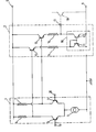
- an amplifier circuit arrangement comprises first and second stages 1 and 2 in cascade.
- the first stage 1 comprises a long tail pair of npn transistors 3 and 4 the collector electrodes of which are connected to a first voltage reference point 5 via first and second resistors 6 and 7 respectively.
- the commoned emitters of the transistors 3 and 4 are connected to a second voltage reference point 8 via a current source 9.
- the second stage 2 comprises a current amplifier circuit 10 which takes the form of a so-called current mirror circuit.
- Circuit 10 comprises a pair of npn transistors 11 and 12 the emitters of which are commoned and connected to the point 8. The bases of these transistors are also commoned and connected to the collector of transistor 11.
- the input current path of circuit 10 extends from the collector/base of transistor 11 to point 8, and the output current path thereof extends from the collector of transistor 12 to point 8.
- the collector end of resistor 6 is connected to the collector/bases of transistor 11 via the base-emitter path of an npn transistor 13 and a third resistor 14, in that order, and the collector end of resistor 7 is connected to the collector of transistor 12 via the base-emitter path of a transistor 15 and a fourth resistor 16, in that order.
- the collectors of transistors 13 and 15 are connected to point 8.
- the common point of resistor 16 and the collector of transistor 12 constitutes the output 17 of the stage 2, and may be connected to the base of a further npn transistor 18 if desired, as indicated in dashed lines.
- a positive supply potential is applied to point 5′ relative to point 8 and an input signal is applied between the bases of transistors 3 and 4 (points 19 and 20 respectively).
- the resulting differential signal voltages appearing at the collectors of the transistors 3 and 4 are applied to the input current path of amplifier 10 via emitter follower transistor 13 and resistor 14, and to the common point of the output current path of amplifier 10 and output terminal 17 via emitter follower transistor 15 and resistor 16, respectively.
- the resulting signal current flowing in the input path of amplifier 10 results in known manner in G times this signal current flowing in the output path of amplifier 10. The overall result is therefore that the output signal of stage 1 is successfully coupled to the output 17 of stage 2.
- the emitter follower transistors 13 and 15, which in effect constitute signal voltage sources of internal resistances R6/(1+B13) and R7/(1+B15) respectively connected between the ends of the resistors 14 and 16 and the point 5, are provided basically to reduce the load imposed on the output of stage 1 by the input of stage 2.
- respective capacitors may be provided across each of the resistors 14 and 16 to improve the frequency response of the arrangement. If such are provided the ratio between their impedances should be chosen equal to the ratio between the corresponding resistors 14 and 16.
- npn transistors in the circuits described may be replaced by pnp transistors if the sign of the supply voltage applied between points 5 and 8 is reversed. Alternatively they may be replaced by n-channel (or p-channel if the sign of the supply voltage is reversed) field effect transistors, the gates, drains and sources of the latter corresponding to the bases, collectors and emitters respectively of the bipolar transistors described.
- the simple current mirror construction shown for the amplifier 10 may of course be replaced by another form of current amplifier circuit, for example one of the many other current mirror circuits which are well-known to persons skilled in the art.
Description
- This invention relates to an amplifier circuit arrangement having first and second stages in cascade, the first stage comprising a long tail pair of first and second transistors of the same conductivity type and first and second resistors coupling output electrodes of said first and second transistors respectively to a first voltage reference point and the second stage comprising a current amplifier circuit and a third resistor, the output electrode end of said first resistor being coupled to a second voltage reference point via said third resistor and the input current path of said current amplifier circuit in that order, and the output electrode end of said second resistor being coupled to said second voltage reference point via the output current path of said current amplifier circuit.
- Long tail pairs of transistors are often employed in amplifier circuit arrangements, particularly when the arrangements are in integrated circuit form. Individual integrated circuit manufacturing techniques tend to favour the fabrication of transistors of a particular conductivity type rather than transistors of the opposite conductivity type, for example because those of the particular conductivity type take the form of so-called "vertical" transistor structures whereas those of the opposite conductivity type take the form of so-called "lateral" transistors. "Vertical" transistor structures tend to have higher gains and cut-off frequencies than "lateral" transistor structures, with the result that in many applications it is usual to try to avoid employing "lateral" transistors if at all possible. However, sometimes other considerations come into play which militate against this. One of these is a requirement in some applications that noise superimposed on the supply voltage of the arrangement must not, or must only negligibly, become manifest in the output signal of the arrangement. An amplifier arrangement of the general kind specified in the first paragraph is known from US-A-4,710,728. In this known amplifier the (differential) output of the first stage is constituted by the output electrode ends of the first and second resistors. Signal voltages occurring at these points are, of course, relative to the first voltage reference point, because they are set up across the first and second resistors respectively. Thus if a said signal voltage were applied to the control electrode of a third transistor the common electrode of which is connected to the first voltage reference point any noise occurring at the first voltage reference point will not have any effect on the signal occurring between said control and common electrodes. However this would mean in practice that, unless the provision for example of more than two supply potentials could be tolerated, the third transistor would have to be of the opposite conductivity type to said same conductivity type, which as stated above is often unsatisfactory. It is an object of the invention to enable this problem to be mitigated.
- According to the invention, an amplifier circuit arrangement as defined in the first paragraph is characterised in that a fourth resistor is included in series between the output electrode end of the second resistor and the output current path of the current amplifier circuit, in that the output current path end of said fourth resistor constitutes an output of the second stage, and in that the resistance values of said first, second, third and fourth resistors, and the gain of said current amplifier, are chosen such that in operation the voltage at the output of the second stage is substantially independent of variations in the potential on the first voltage reference point relative to the potential on the second voltage reference point.
- A paper by Carlos A. Laber et al entitled Design Considerations for a High-Performance 3-µm CMOS Analogue Standard-Cell Library published in IEEE Journal of Solid State Circuits, Vol. SC-22, No. 2, April 1987 at pages 181 to 189 discloses in Figure 6a) on page 186 a circuit configuration as set forth in the first and preceding paragraphs.
- It has now been recognised that if it is arranged that the second stage has a circuit configuration as set forth, then with a suitable choice of the values of the resistors and the gain of the current amplifier, the output signal of the first stage can be coupled to the output of the second stage in such manner that any noise occurring at the first voltage reference point relative to the second voltage reference point will have little or no effect on the signal occurring at the output of the second stage, relative to the second voltage reference point. If the sign of the voltage between the first and second voltage reference points is appropriately chosen the signal at the output of the second stage (which stage may itself include transistors all of which are of said same conductivity type) can be applied in turn, for example, to the control electrode of a further transistor of said same conductivity type the common electrode of which is connected to the second voltage reference point (to which the "tail" of the long tail pair may conveniently be connected).
- The terms "control electrode", "output electrode" and "common electrode" are to be understood to mean herein "base electrode", "collector electrode" and "emitter electrode" respectively if the relevant transistor is a bipolar transistor, and to mean "gate electrode", "drain electrode" and "source electrode" respectively if the relevant transistor is a field-effect transistor. The gain G of the current amplifier stage may, or course, be less than, equal to, or greater than unity.
- The second stage may include third and fourth transistors of said same conductivity type, the output electrodes of said third and fourth transistors being connected to said first voltage reference point, and the control electrode/common electrode paths of said third and fourth transistors being included between said output electrode end of said first resistor and said third resistor, and between said output electrode end of said second resistor and said fourth resistor, respectively. On the other hand if the values of the third and fourth resistors are high relative to the values of the first and second resistors respectively the third and fourth resistors may be connected directly to the first and second resistors respectively.
- Embodiments of the invention will now be described, by way of example, with reference to the accompanying diagrammatic drawing the single Figure of which is a circuit diagram of a particular embodiment.
- In the drawing an amplifier circuit arrangement comprises first and second stages 1 and 2 in cascade. The first stage 1 comprises a long tail pair of npn transistors 3 and 4 the collector electrodes of which are connected to a first voltage reference point 5 via first and second resistors 6 and 7 respectively. The commoned emitters of the transistors 3 and 4 are connected to a second voltage reference point 8 via a
current source 9. The second stage 2 comprises a current amplifier circuit 10 which takes the form of a so-called current mirror circuit. Circuit 10 comprises a pair ofnpn transistors transistor 11. The input current path of circuit 10 extends from the collector/base oftransistor 11 to point 8, and the output current path thereof extends from the collector oftransistor 12 to point 8. The collector end of resistor 6 is connected to the collector/bases oftransistor 11 via the base-emitter path of an npn transistor 13 and a third resistor 14, in that order, and the collector end of resistor 7 is connected to the collector oftransistor 12 via the base-emitter path of atransistor 15 and a fourth resistor 16, in that order. The collectors oftransistors 13 and 15 are connected to point 8. The common point of resistor 16 and the collector oftransistor 12 constitutes theoutput 17 of the stage 2, and may be connected to the base of afurther npn transistor 18 if desired, as indicated in dashed lines. The resistance values R₆, R₇, R₁₄ and R₁₆ of the resistors 6, 7, 14 and 16 respectively, together with the current gain G of amplifier 10, are chosen in relation to the current gains B₁₃ and B₁₅ oftransistors 13 and 15 respectively such that the equation
- In operation a positive supply potential is applied to point 5′ relative to point 8 and an input signal is applied between the bases of transistors 3 and 4 (
points 19 and 20 respectively). The resulting differential signal voltages appearing at the collectors of the transistors 3 and 4 are applied to the input current path of amplifier 10 via emitter follower transistor 13 and resistor 14, and to the common point of the output current path of amplifier 10 andoutput terminal 17 viaemitter follower transistor 15 and resistor 16, respectively. The resulting signal current flowing in the input path of amplifier 10 results in known manner in G times this signal current flowing in the output path of amplifier 10. The overall result is therefore that the output signal of stage 1 is successfully coupled to theoutput 17 of stage 2. - If this potential at point 5 should vary relative to that on point 8, the base current of transistor 13 will vary by i, say. This will result in a change of i(1+B₁₃) in the emitter current of transistor 13 and hence in the currents through resistor 14 and the input current path of amplifier 10. The result is therefore a change of Gi(1+B₁₃) in the output current of amplifier 10 and hence in the emitter current of
transistor 15 and the current through resistor 16. The resulting change in the base current oftransistor 15 is therefore Gi(1+B₁₃)/(1+B₁₅). The change in the potential atoutput terminal 17 relative to point 5 is therefore R₇Gi(1+B₁₃)/(1+B₁₅) + R₁₆Gi(1+B₁₃). However the change v in the potential on point 5 relative to that on point 8 is given by v = R₆i + R₁₄i(1+B₁₃). As has been mentioned previously, R₆, R₇, R₁₄, R₁₆ and G have been chosen relative to B₁₃ and B₁₅ such that the equation
output terminal 17 relative to point 5 is itself substantially equal to v. In other words, the change in the potential atoutput terminal 17 relative to point 8 is substantially zero, as required. - The
emitter follower transistors 13 and 15, which in effect constitute signal voltage sources of internal resistances R₆/(1+B₁₃) and R₇/(1+B₁₅) respectively connected between the ends of the resistors 14 and 16 and the point 5, are provided basically to reduce the load imposed on the output of stage 1 by the input of stage 2. If the values of resistors 14 and 16 are high relative to the values of resistors 6 and 7 respectively these emitter followers may be omitted, resistor 14 then being connected directly to the collector end of resistor 6 and resistor 16 being connected directly to the collector end of resistor 7 so that resistors 6 and 7 now themselves effectively constitute signal voltage sources of internal resistances R₆ and R₇ respectively connected between the ends of the resistors 14 and 16 and the point 5 when driven by the long tail pair transistors. If this is done the result is equivalent to writing B₁₃ = B₁₅ = 0 in the expression quoted above, which in consequence reduces to
- If desired, respective capacitors, possibly in series with respective resistors, may be provided across each of the resistors 14 and 16 to improve the frequency response of the arrangement. If such are provided the ratio between their impedances should be chosen equal to the ratio between the corresponding resistors 14 and 16.
- Obviously the npn transistors in the circuits described may be replaced by pnp transistors if the sign of the supply voltage applied between points 5 and 8 is reversed. Alternatively they may be replaced by n-channel (or p-channel if the sign of the supply voltage is reversed) field effect transistors, the gates, drains and sources of the latter corresponding to the bases, collectors and emitters respectively of the bipolar transistors described. The simple current mirror construction shown for the amplifier 10 may of course be replaced by another form of current amplifier circuit, for example one of the many other current mirror circuits which are well-known to persons skilled in the art.
- From reading the present disclosure, other modifications will be apparent to persons skilled in the art. Such modifications may involve other features which are already known in the design, manufacture and use of circuit arrangements and component parts thereof and which may be used instead of or in addition to features already described herein.
Claims (5)
- An amplifier circuit arrangement having first and second stages in cascade, the first stage comprising a long tail pair of first and second transistors of the same conductivity type and first and second resistors coupling output electrodes of said first and second transistors respectively to a first voltage reference point and the second stage comprising a current amplifier circuit and a third resistor, the output electrode end of said first resistor being coupled to a second voltage reference point via said third resistor and the input current path of said current amplifier circuit in that order, and the output electrode end of said second resistor being coupled to said second voltage reference point via the output current path of said current amplifier circuit, characterised in that a fourth resistor is included in series between the output electrode end of the second resistor and the output current path of the current amplifier circuit, in that the output current path end of said fourth resistor constitutes an output of the second stage, and in that the resistance values of said first, second, third and fourth resistors, and the gain of said current amplifier, are chosen such that in operation the voltage at the output of the second stage is substantially independent of variations in the potential on the first voltage reference point relative to the potential on the second voltage reference point.
- An arrangement as claimed in Claim 1, wherein the second stage includes transistors all of which are of said same conductivity type.
- An arrangement as claimed in Claim 1 or Claim 2, wherein the second stage includes third and fourth transistors of said same conductivity type, the output electrodes of said third and fourth transistors being connected to said first voltage reference point, and the control electrode/common electrode paths of said third and fourth transistors being included between said output electrode end of said first resistor and said third resistor, and between said output electrode end of said second resistor and said fourth resistor, respectively.
- An arrangement as claimed in Claim 1 or Claim 2, wherein the resistance values of said third and fourth resistors are high relative to the resistance values of said first and second resistors respectively and the third and fourth resistors are connected directly to the first and second resistors respectively.
- An arrangement as claimed in any preceding Claim, wherein the tail of the long tail pair is connected to the second voltage reference point.
Applications Claiming Priority (2)
| Application Number | Priority Date | Filing Date | Title |
|---|---|---|---|
| GB8730137 | 1987-12-24 | ||
| GB8730137A GB2214375A (en) | 1987-12-24 | 1987-12-24 | Amplifier circuit arrangement |
Publications (3)
| Publication Number | Publication Date |
|---|---|
| EP0324205A2 EP0324205A2 (en) | 1989-07-19 |
| EP0324205A3 EP0324205A3 (en) | 1990-09-19 |
| EP0324205B1 true EP0324205B1 (en) | 1996-03-27 |
Family
ID=10629049
Family Applications (1)
| Application Number | Title | Priority Date | Filing Date |
|---|---|---|---|
| EP88202944A Expired - Lifetime EP0324205B1 (en) | 1987-12-24 | 1988-12-19 | Amplifier circuit arrangement |
Country Status (5)
| Country | Link |
|---|---|
| US (1) | US4920321A (en) |
| EP (1) | EP0324205B1 (en) |
| JP (1) | JP2774120B2 (en) |
| DE (1) | DE3855157T2 (en) |
| GB (1) | GB2214375A (en) |
Families Citing this family (5)
| Publication number | Priority date | Publication date | Assignee | Title |
|---|---|---|---|---|
| US5510745A (en) * | 1987-07-29 | 1996-04-23 | Fujitsu Limited | High-speed electronic circuit having a cascode configuration |
| US5304869A (en) * | 1992-04-17 | 1994-04-19 | Intel Corporation | BiCMOS digital amplifier |
| JPH07111484A (en) * | 1993-08-20 | 1995-04-25 | Hitachi Ltd | Radio communication equipment |
| US5917349A (en) * | 1997-10-09 | 1999-06-29 | Kabushiki Kaisha Toshiba | Current mode driver using N-type transistors |
| JP2002057532A (en) * | 2000-08-11 | 2002-02-22 | Nec Corp | Linear transconductance amplifier |
Family Cites Families (7)
| Publication number | Priority date | Publication date | Assignee | Title |
|---|---|---|---|---|
| US3444476A (en) * | 1965-03-19 | 1969-05-13 | Rca Corp | Direct coupled amplifier with feedback for d.c. error correction |
| FR1529717A (en) * | 1967-04-19 | 1968-06-21 | Sfim | Direct-Link DC Differential Amplifier |
| JPS6090407A (en) * | 1983-10-24 | 1985-05-21 | Toshiba Corp | Differential amplifier |
| JPS62274923A (en) * | 1986-05-23 | 1987-11-28 | Hitachi Ltd | Semiconductor device |
| US4710728A (en) * | 1986-06-30 | 1987-12-01 | Motorola, Inc. | Amplifier having improved gain-bandwidth product |
| US4767946A (en) * | 1987-01-12 | 1988-08-30 | Tektronix, Inc. | High-speed supply independent level shifter |
| JPS63240109A (en) * | 1987-03-27 | 1988-10-05 | Toshiba Corp | Differential amplifier |
-
1987
- 1987-12-24 GB GB8730137A patent/GB2214375A/en not_active Withdrawn
-
1988
- 1988-12-19 DE DE3855157T patent/DE3855157T2/en not_active Expired - Fee Related
- 1988-12-19 EP EP88202944A patent/EP0324205B1/en not_active Expired - Lifetime
- 1988-12-22 US US07/289,650 patent/US4920321A/en not_active Expired - Lifetime
- 1988-12-23 JP JP63323772A patent/JP2774120B2/en not_active Expired - Lifetime
Non-Patent Citations (1)
| Title |
|---|
| Journal of Solid State Electronics, vol.SC-22, no.2, April 1987. * |
Also Published As
| Publication number | Publication date |
|---|---|
| GB8730137D0 (en) | 1988-02-03 |
| EP0324205A3 (en) | 1990-09-19 |
| DE3855157T2 (en) | 1996-10-02 |
| DE3855157D1 (en) | 1996-05-02 |
| GB2214375A (en) | 1989-08-31 |
| US4920321A (en) | 1990-04-24 |
| EP0324205A2 (en) | 1989-07-19 |
| JP2774120B2 (en) | 1998-07-09 |
| JPH01202907A (en) | 1989-08-15 |
Similar Documents
| Publication | Publication Date | Title |
|---|---|---|
| EP0058448B1 (en) | Transconductance amplifier | |
| JPS63107210A (en) | Differential voltage-current converter | |
| EP0600852B1 (en) | Logic circuit arrangements | |
| US4573020A (en) | Fully differential operational amplifier with D.C. common-mode feedback | |
| US4797629A (en) | Wide range operational amplifier input stage | |
| US5469092A (en) | Electronic circuit including means for reflecting signal current and feed forward means for compensating operational speed thereof | |
| US3534279A (en) | High current transistor amplifier stage operable with low current biasing | |
| US5485074A (en) | High ratio current mirror with enhanced power supply rejection ratio | |
| US4912427A (en) | Power supply noise rejection technique for amplifiers | |
| US5332937A (en) | Transconductor stage for high frequency filters | |
| US4978868A (en) | Simplified transistor base current compensation circuitry | |
| EP0324205B1 (en) | Amplifier circuit arrangement | |
| US4890067A (en) | Common base configuration for an fT doubler amplifier | |
| JPH0550163B2 (en) | ||
| US4779057A (en) | Cascode amplifier with nonlinearity correction and improve transient response | |
| US4550291A (en) | Noise-free, die area efficient cascode circuit | |
| EP0164182B1 (en) | Jfet active load input stage | |
| CN116895320A (en) | Device for reproducing current | |
| US4730124A (en) | High transconductance composite PNP transistor | |
| US4928073A (en) | DC amplifier | |
| US5334949A (en) | Differential amplifiers | |
| US5144169A (en) | Operational amplifier circuit | |
| US4137506A (en) | Compound transistor circuitry | |
| US6339319B1 (en) | Cascoded current mirror circuit | |
| JPH0645844A (en) | Differential amplifier |
Legal Events
| Date | Code | Title | Description |
|---|---|---|---|
| PUAI | Public reference made under article 153(3) epc to a published international application that has entered the european phase |
Free format text: ORIGINAL CODE: 0009012 |
|
| AK | Designated contracting states |
Kind code of ref document: A2 Designated state(s): DE FR GB IT NL |
|
| PUAL | Search report despatched |
Free format text: ORIGINAL CODE: 0009013 |
|
| AK | Designated contracting states |
Kind code of ref document: A3 Designated state(s): DE FR GB IT NL |
|
| 17P | Request for examination filed |
Effective date: 19910315 |
|
| RAP3 | Party data changed (applicant data changed or rights of an application transferred) |
Owner name: N.V. PHILIPS' GLOEILAMPENFABRIEKEN Owner name: PHILIPS ELECTRONICS UK LIMITED |
|
| 17Q | First examination report despatched |
Effective date: 19930210 |
|
| GRAA | (expected) grant |
Free format text: ORIGINAL CODE: 0009210 |
|
| AK | Designated contracting states |
Kind code of ref document: B1 Designated state(s): DE FR GB IT NL |
|
| PG25 | Lapsed in a contracting state [announced via postgrant information from national office to epo] |
Ref country code: NL Free format text: LAPSE BECAUSE OF FAILURE TO SUBMIT A TRANSLATION OF THE DESCRIPTION OR TO PAY THE FEE WITHIN THE PRESCRIBED TIME-LIMIT Effective date: 19960327 |
|
| REF | Corresponds to: |
Ref document number: 3855157 Country of ref document: DE Date of ref document: 19960502 |
|
| ITF | It: translation for a ep patent filed |
Owner name: ING. C. GREGORJ S.P.A. |
|
| ET | Fr: translation filed | ||
| NLV1 | Nl: lapsed or annulled due to failure to fulfill the requirements of art. 29p and 29m of the patents act | ||
| PLBE | No opposition filed within time limit |
Free format text: ORIGINAL CODE: 0009261 |
|
| STAA | Information on the status of an ep patent application or granted ep patent |
Free format text: STATUS: NO OPPOSITION FILED WITHIN TIME LIMIT |
|
| 26N | No opposition filed | ||
| REG | Reference to a national code |
Ref country code: FR Ref legal event code: CD |
|
| PGFP | Annual fee paid to national office [announced via postgrant information from national office to epo] |
Ref country code: DE Payment date: 20010214 Year of fee payment: 13 |
|
| PGFP | Annual fee paid to national office [announced via postgrant information from national office to epo] |
Ref country code: FR Payment date: 20011221 Year of fee payment: 14 |
|
| PGFP | Annual fee paid to national office [announced via postgrant information from national office to epo] |
Ref country code: GB Payment date: 20011224 Year of fee payment: 14 |
|
| REG | Reference to a national code |
Ref country code: GB Ref legal event code: IF02 |
|
| PG25 | Lapsed in a contracting state [announced via postgrant information from national office to epo] |
Ref country code: DE Free format text: LAPSE BECAUSE OF NON-PAYMENT OF DUE FEES Effective date: 20020702 |
|
| PG25 | Lapsed in a contracting state [announced via postgrant information from national office to epo] |
Ref country code: GB Free format text: LAPSE BECAUSE OF NON-PAYMENT OF DUE FEES Effective date: 20021219 |
|
| GBPC | Gb: european patent ceased through non-payment of renewal fee |
Effective date: 20021219 |
|
| PG25 | Lapsed in a contracting state [announced via postgrant information from national office to epo] |
Ref country code: FR Free format text: LAPSE BECAUSE OF NON-PAYMENT OF DUE FEES Effective date: 20030901 |
|
| REG | Reference to a national code |
Ref country code: FR Ref legal event code: ST |
|
| PG25 | Lapsed in a contracting state [announced via postgrant information from national office to epo] |
Ref country code: IT Free format text: LAPSE BECAUSE OF NON-PAYMENT OF DUE FEES;WARNING: LAPSES OF ITALIAN PATENTS WITH EFFECTIVE DATE BEFORE 2007 MAY HAVE OCCURRED AT ANY TIME BEFORE 2007. THE CORRECT EFFECTIVE DATE MAY BE DIFFERENT FROM THE ONE RECORDED. Effective date: 20051219 |