EP0321663A2 - Protection circuitry for a commutating transistor - Google Patents
Protection circuitry for a commutating transistor Download PDFInfo
- Publication number
- EP0321663A2 EP0321663A2 EP88116306A EP88116306A EP0321663A2 EP 0321663 A2 EP0321663 A2 EP 0321663A2 EP 88116306 A EP88116306 A EP 88116306A EP 88116306 A EP88116306 A EP 88116306A EP 0321663 A2 EP0321663 A2 EP 0321663A2
- Authority
- EP
- European Patent Office
- Prior art keywords
- voltage
- switching transistor
- circuit arrangement
- pulse width
- width modulator
- Prior art date
- Legal status (The legal status is an assumption and is not a legal conclusion. Google has not performed a legal analysis and makes no representation as to the accuracy of the status listed.)
- Granted
Links
Images

Classifications
-
- H—ELECTRICITY
- H02—GENERATION; CONVERSION OR DISTRIBUTION OF ELECTRIC POWER
- H02H—EMERGENCY PROTECTIVE CIRCUIT ARRANGEMENTS
- H02H9/00—Emergency protective circuit arrangements for limiting excess current or voltage without disconnection
- H02H9/04—Emergency protective circuit arrangements for limiting excess current or voltage without disconnection responsive to excess voltage
-
- H—ELECTRICITY
- H02—GENERATION; CONVERSION OR DISTRIBUTION OF ELECTRIC POWER
- H02P—CONTROL OR REGULATION OF ELECTRIC MOTORS, ELECTRIC GENERATORS OR DYNAMO-ELECTRIC CONVERTERS; CONTROLLING TRANSFORMERS, REACTORS OR CHOKE COILS
- H02P7/00—Arrangements for regulating or controlling the speed or torque of electric DC motors
- H02P7/06—Arrangements for regulating or controlling the speed or torque of electric DC motors for regulating or controlling an individual DC dynamo-electric motor by varying field or armature current
- H02P7/18—Arrangements for regulating or controlling the speed or torque of electric DC motors for regulating or controlling an individual DC dynamo-electric motor by varying field or armature current by master control with auxiliary power
- H02P7/24—Arrangements for regulating or controlling the speed or torque of electric DC motors for regulating or controlling an individual DC dynamo-electric motor by varying field or armature current by master control with auxiliary power using discharge tubes or semiconductor devices
- H02P7/28—Arrangements for regulating or controlling the speed or torque of electric DC motors for regulating or controlling an individual DC dynamo-electric motor by varying field or armature current by master control with auxiliary power using discharge tubes or semiconductor devices using semiconductor devices
- H02P7/285—Arrangements for regulating or controlling the speed or torque of electric DC motors for regulating or controlling an individual DC dynamo-electric motor by varying field or armature current by master control with auxiliary power using discharge tubes or semiconductor devices using semiconductor devices controlling armature supply only
- H02P7/288—Arrangements for regulating or controlling the speed or torque of electric DC motors for regulating or controlling an individual DC dynamo-electric motor by varying field or armature current by master control with auxiliary power using discharge tubes or semiconductor devices using semiconductor devices controlling armature supply only using variable impedance
-
- H—ELECTRICITY
- H03—ELECTRONIC CIRCUITRY
- H03K—PULSE TECHNIQUE
- H03K17/00—Electronic switching or gating, i.e. not by contact-making and –breaking
- H03K17/08—Modifications for protecting switching circuit against overcurrent or overvoltage
- H03K17/082—Modifications for protecting switching circuit against overcurrent or overvoltage by feedback from the output to the control circuit
- H03K17/0822—Modifications for protecting switching circuit against overcurrent or overvoltage by feedback from the output to the control circuit in field-effect transistor switches
Definitions
- the invention relates to a circuit arrangement for protecting a switching transistor, the type specified in the preamble of claim 1.
- the breakdown voltage is dimensioned in such a way that it is not normally exceeded by the supply voltage present plus the resulting switching voltage due to line and leakage inductances.
- voltage limiter components such as varistors or zener diodes
- Such voltage limiter components must be dimensioned large in order to absorb high-energy overvoltage pulses and to be able to dissipate the resulting power loss.
- the switching transistor is generally able to dissipate greater power losses than the voltage limiter components can.
- the switching transistor also has only a limited ability to dissipate the power loss that arises in the event of overvoltages. Overvoltages that persist for a long time, e.g. the supply voltage is directly dependent on the mains voltage, lead to the destruction of the switching transistor.
- the object of the invention is therefore to provide a circuit arrangement of the type mentioned at the outset, which on the one hand actively and reliably protects the switching transistor from overvoltages, and on the other hand avoids a complete switch-off in the event of an overload.
- the invention is therefore based on the idea of having the switching transistor continue to switch if the supply voltage continues to overvoltage, but to reduce the switching voltage which arises. Since the level of the switching voltage with a constant switching time depends on the level of the current through the line or leakage inductances, the switching voltage is reduced by reducing the current. This is achieved by influencing the pulse width modulator, which is triggered in the event of a fault by the control signal additionally obtained in such a way that the pulse-pause ratio with which the switching transistor is controlled is reduced.
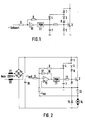
- a Zener diode 1 is connected with its cathode as a voltage limiting element, which is connected on the anode side to a capacitor 7 via a diode 4.
- a line branch with a discharge resistor 8 is connected between the capacitor 7 and the diode 4, which leads to a summation point at the input of a current regulator 10.
- This summation point is connected to a setpoint generator via a resistor 9.
- a differential voltage is formed from the setpoint signal and the voltage which is present at the summation point via the discharge resistor 8 and is applied to the current regulator.
- the current regulator 10 is connected to the control input of a pulse width modulator 11, which is connected to the control input of the switching transistor 2 on the output side.
- the zener diode 1 is connected with its anode via a diode 3 and a second zener diode 6 directly bypassing the pulse width modulator 11 to the control input of the switching transistor 2.
- the control input of the switching transistor 2 is connected to the ground potential via a further Zener diode 5.
- the Zener diode 1 becomes conductive as a voltage limiter diode.
- the current flowing through the voltage limiter diode 1 charges the capacitor 4 via the diode 4.
- the discharge current of the capacitor reduces the pulse-pause ratio of the pulse width modulator 11 via the discharge resistor 8. As a result, the switching current through the switching transistor 2 and thus the switching voltage is reduced with the next clock cycles.
- the discharge time constant of the capacitor 7 is chosen to be very large compared to the cycle period, stable operating points are set in accordance with the level of the static supply overvoltage.
- the capacitor 7 is charged faster than the current in the load can be reduced by changing the pulse-pause ratio.
- the switching transistor is driven via the diode 3 and the zener diode 6.
- the overvoltage is itself limited by the switching transistor 2, which is conductive in the activated state.
- the breakdown voltage of the Zener diode 6 is dimensioned so that the capacitor 7 can charge until the pulse-pause ratio of the pulse width modulator 11 becomes zero when the switching oil sistor 2 is switched on for dynamic overvoltage limitation. Due to the long discharge time constant of the capacitor 7, the switching transistor 2 is given a recovery time in order to dissipate the power loss absorbed during the overvoltage limitation.
- FIG. 2 shows an analog circuit arrangement on a 20 kHz motor current regulator.
- the basic structure and function of this circuit arrangement is the same as that shown in FIG. 1.
- the motor 14 is fed from the network via a rectifier bridge 20 and the switching transistor 2.
- the motor current is detected via the current measuring resistor 13 and regulated by the current controller 10 to the predetermined target value.
- a control signal is also formed here via the limiter diode 1 and the diode 4 by means of the capacitor 7, which is given via the discharge resistor 8 to the summation point of the current regulator.
- the current regulator 10 reduces the motor current just enough that a maximum voltage at the switching transistor 2 is not exceeded.
- FIG. 3 shows the dependency of the motor current on the level of the static mains voltage, which results in the circuit arrangement according to FIG. 2.
- a diode with a breakdown voltage of 440 V was used as the limiter diode.
- the motor can be supplied with maximum current up to a mains voltage of 260 V.
- the motor current is reduced by the circuit arrangement described above.
- a - D in Fig. 3 is shown in Fig. 4, the voltage at the switching transistor 2 at the respective line voltages. From this it can be seen that at mains voltages above 260 V the motor current is reduced just enough that the voltage at the switching transistor corresponds to the breakdown voltage of 440 V of the Zener diode 1.
- the proportion of the switching voltage is thus reduced by reducing the motor current when the mains voltage increases.
- the maximum voltage at switching transistor 2 is kept at a constant value.
- the decisive advantage when using the circuit arrangement described above is that only the motor current and thus the motor torque is reduced in the motor current control for the duration of the mains overvoltage. Overloading the switching transistor 2 on the one hand and stopping the drive on the other hand is avoided with this circuit arrangement.
Landscapes
- Engineering & Computer Science (AREA)
- Power Engineering (AREA)
- Dc-Dc Converters (AREA)
- Electronic Switches (AREA)
- Emergency Protection Circuit Devices (AREA)
- Protection Of Static Devices (AREA)
- Power Conversion In General (AREA)
- Control Of Motors That Do Not Use Commutators (AREA)
Abstract
Die Erfindung bezieht sich auf eine Schaltungsanordnung zum Schutz eines Schalttransistors, der zwischen einer Gleichspannungsquelle und einer induktiven Last angeordnet ist, mit einem steuerbaren Pulbreitenmodulator, der den Schalttransistor ansteuert, und mit einem Spannungsbegrenzungsbauelemten, das bei auftretenden Überspannungen ein Einschalten des Transistors bewirkt.The invention relates to a circuit arrangement for protecting a switching transistor, which is arranged between a DC voltage source and an inductive load, with a controllable pulse width modulator, which controls the switching transistor, and with a voltage limiting component, which causes the transistor to be switched on when overvoltages occur.
Eine solche Schaltungsanordnung soll nun einerseits den Schalttransistor aktiv und zuverlässig vor Überspannungen schützen und andererseits im Überlastungsfall ein vollständiges Abschalten vermeiden.Such a circuit arrangement is now intended on the one hand to actively and reliably protect the switching transistor from overvoltages and on the other hand to avoid complete switching off in the event of an overload.
Dazu wird mittels des Spannungsbegrenzerbauelementes zusätzlich ein Regelsignal gewonnen, das an den Steuereingang des Pulsbreitenmodulators derart angelegt wird, daß das Puls-Pause-Verhältnis des Pulsbreitenmodulators bei Überspannungen verringert wird. 
Description
Die Erfindung bezieht sich auf eine Schaltungsanordnung zum Schutz eines Schalttransistors, der im Gattungsbegriff des Patentanspruchs 1 näher bezeichneten Art.The invention relates to a circuit arrangement for protecting a switching transistor, the type specified in the preamble of
Bei Schalttransistoren wird die Durchbruchspannung so bemessen, daß sie im Normalfall von der anliegenden Versorgungsspannung zuzüglich der entstehenden Schaltspannung durch Leitungs- und Streuinduktivitäten nicht überschritten wird. Es wäre jedoch unwirtschaftlich, die Durchbruchspannung von Schalttransistoren so groß zu wählen, daß noch die höchste je auftretende Überspannung unterhalb der Durchbruchspannung bleibt. Man muß deshalb Schutzschaltungen vorsehen, über die auftretende Überspannungen, die größer als die Durchbruchspannung sind, abgeleitet werden, um den Schalttransistor vor solchen gelegentlich auftretenden Überspannungen zu schützen.In the case of switching transistors, the breakdown voltage is dimensioned in such a way that it is not normally exceeded by the supply voltage present plus the resulting switching voltage due to line and leakage inductances. However, it would be uneconomical to choose the breakdown voltage of switching transistors so large that the highest overvoltage ever occurring remains below the breakdown voltage. It is therefore necessary to provide protective circuits through which the overvoltages that occur which are greater than the breakdown voltage are derived in order to protect the switching transistor from such overvoltages that occasionally occur.
Dazu ist es bekannt, parallel zum Schalttransistor Spannungsbegrenzerbauelemente, wie Varistoren oder Zenerdioden, anzuordnen. Solche Spannungsbegrenzerbauelemente müssen groß dimensioniert werden, um energiereiche Überspannungspulse aufzunehmen und die entstehende Verlustleistung abführen zu können.For this purpose, it is known to arrange voltage limiter components, such as varistors or zener diodes, parallel to the switching transistor. Such voltage limiter components must be dimensioned large in order to absorb high-energy overvoltage pulses and to be able to dissipate the resulting power loss.
Im Hinblick auf die Dimensionierung der Bauteile der Schutzschaltung ist es vorteilhafter, den Transistor mittels einer Zenerdiode oder einem Varistor bei auftretenden Überspannungen einzuschalten. Denn hierfür sind nur kleine Spannungsbegrenzerbauelemente erforderlich, da die Energie der Überspannungspulse vom Transistor selbst aufgenommen wird. Der Schalttransistor ist in der Regel in der Lage, größere Verlustleistungen abzuführen, als es die Spannungsbegrenzerbauelemente können.With regard to the dimensioning of the components of the protective circuit, it is more advantageous to switch on the transistor by means of a zener diode or a varistor when overvoltages occur. Because only small voltage limiter components are required for this, since the energy of the overvoltage pulses from Transistor itself is included. The switching transistor is generally able to dissipate greater power losses than the voltage limiter components can.
Letztlich hat aber auch der Schalttransistor nur ein begrenztes Vermögen, die bei Überspannungen entstehende Verlustleistung abzuführen. So können Überspannungen, die für längere Zeit anstehen, wenn z.B. die Versorgungsspannung direkt netzspannungsabhängig ist, zur Zerstörung des Schalttransistors führen.Ultimately, however, the switching transistor also has only a limited ability to dissipate the power loss that arises in the event of overvoltages. Overvoltages that persist for a long time, e.g. the supply voltage is directly dependent on the mains voltage, lead to the destruction of the switching transistor.
Um aufgrund einer solchen Dauerbeanspruchung mit Überspannung eine Zerstörung des Transistors zu vermeiden, ist es ferner bekannt, die Überspannung durch eine Messeinrichtung zu erfassen. Bei Überschreiten eines maximalen Spannungspegels wird eine Impulssperre des Pulsbreitenmodulators ausgelöst, wonach der Schalttransistor nicht mehr angesteuert wird und ein erneutes Einschalten des Transistors verhindert ist. Infolge dessen wird die Spannung am Schalttransistor um die Schaltspannung reduziert. Zwar wird durch diese zusätzliche Maßnahme eine Überlastung des Schalttransistors bei länger andauernder Versorgungsüberspannung, die durch die ständige aktive Begrenzung der Schaltspannung entstehen würde, sicher vermieden, nachteilig dabei ist jedoch, daß ein solcher Störfall zu einer vollständigen Abschaltung führt. Wird z.B. über den Schalttransistor ein Gleichstrommotor versorgt, führte der beschriebene Überspannungsfall jeweils zum Stillsitzen des Antriebs. In den meisten Einsatzfällen ist dies nicht akzeptabel.In order to avoid destruction of the transistor due to such permanent stress with overvoltage, it is also known to detect the overvoltage by means of a measuring device. If a maximum voltage level is exceeded, a pulse lock of the pulse width modulator is triggered, after which the switching transistor is no longer activated and the transistor is prevented from being switched on again. As a result, the voltage at the switching transistor is reduced by the switching voltage. Overloading the switching transistor in the event of a prolonged supply overvoltage, which would result from the constant active limitation of the switching voltage, is certainly avoided by this additional measure, but it is disadvantageous that such a fault leads to a complete shutdown. If, for example, a DC motor is supplied via the switching transistor, the described overvoltage case always led to the drive being stopped. In most cases this is not acceptable.
Aufgabe der Erfindung ist es daher, eine Schaltungsanordnung der eingangs genannten Art zu schaffen, die einerseits den Schalttransistor aktiv und zuverlässig vor Überspannungen schützt, andererseits im Überlastungsfall ein vollständiges Abschalten vermeidet.The object of the invention is therefore to provide a circuit arrangement of the type mentioned at the outset, which on the one hand actively and reliably protects the switching transistor from overvoltages, and on the other hand avoids a complete switch-off in the event of an overload.
Diese Aufgabe wird nach der Erfindung durch die kennzeichnenden Merkmale des Patentanspruchs 1 gelöst.This object is achieved according to the invention by the characterizing features of
Die Erfindung beruht also auf dem Gedanken, bei andauernder Überspannung der Versorgungsspannung den Schalttransistor weiter schalten zu lassen, jedoch die entstehende Schaltspannung zu reduzieren. Da die Höhe der Schaltspannung bei konstanter Schaltzeit von der Höhe des Stromes durch die Leitungs- bzw. Streuinduktivitäten abhängig ist, wird die Schaltspannung durch die Reduzierung des Stromes verringert. Man erreicht dies durch die Einflußnahme auf den Pulsbreitenmodulator, welcher im Störfalle durch das zusätzlich gewonnene Regelsignal derart angesteuert wird, daß das Puls- Pause-Verhältnis, mit dem der Schalttransistor angesteuert wird, verringert wird.The invention is therefore based on the idea of having the switching transistor continue to switch if the supply voltage continues to overvoltage, but to reduce the switching voltage which arises. Since the level of the switching voltage with a constant switching time depends on the level of the current through the line or leakage inductances, the switching voltage is reduced by reducing the current. This is achieved by influencing the pulse width modulator, which is triggered in the event of a fault by the control signal additionally obtained in such a way that the pulse-pause ratio with which the switching transistor is controlled is reduced.
Die Erfindung wird nachfolgend anhand der Zeichnung an Ausführungsbeispielen noch näher erläutert. Dabei zeigen:
- Fig. 1: Das Schaltbild einer Schaltungsanordnung zum Schutz eines Schalttransistors in einer ersten, einfachen Ausführungsform und
- Fig. 2: das Schaltbild einer Schaltungsanordnung der vorgenannten Art bei einem Motorstromregler,
- Fig. 3: ein Diagramm zur Veranschaulichung der Abhängigkeit des Motorstromes von der Höhe der statischen Netzspannung bei der Schaltungsanordnung nach Fig. 2 und
- Fig. 4: die Darstellung der Spannung am Schalttransistor bei verschiedenen Netzspannungen entsprechend der Arbeitspunkte A bis D in Fig. 3.
- Fig. 1: The circuit diagram of a circuit arrangement for protecting a switching transistor in a first, simple embodiment and
- 2: the circuit diagram of a circuit arrangement of the aforementioned type in a motor current regulator,
- 3: a diagram illustrating the dependence of the motor current on the level of the static mains voltage in the circuit arrangement according to FIGS. 2 and
- 4: the representation of the voltage at the switching transistor at different line voltages corresponding to the operating points A to D in FIG. 3.
Im einzelnen zeigt Fig. 1 ein Ausführungsbeispiel für die Schutzschaltungsanordnung eines Schalttransistors, wie sie in einem Schaltnetzteil eingesetzt werden kann. Am Eingangszweig eines Schalttransistors 2 ist als Spannungsbegrenzungsbauglied eine Zenerdiode 1 mit ihrer Katode angeschlossen, die anodenseitig über eine Diode 4 mit einem Kondensator 7 verbunden ist. Zwischen dem Kondensator 7 und der Diode 4 ist ein Leitungszweig mit einem Entladewiderstand 8 angeschlossen, der zu einem Summationspunkt am Eingang eines Stromreglers 10 führt. Dieser Summationspunkt ist über einen Widerstand 9 mit einem Sollwertgeber verbunden. Aus dem Sollwertsignal und der Spannung, die über den Entladewiderstand 8 an dem Summationspunkt anliegt, wird eine Differenzspannung gebildet, die auf den Stromregler gegeben wird. Ausgangsseitig ist der Stromregler 10 mit dem Steuereingang eines Pulsbreitenmodulators 11 verbunden, der ausgangsseitig am Steuereingang des Schalttransistors 2 anliegt.1 shows an exemplary embodiment of the protective circuit arrangement of a switching transistor, as can be used in a switched-mode power supply. At the input branch of a
Weiter ist die Zenerdiode 1 mit ihrer Anode über eine Diode 3 und eine zweite Zenerdiode 6 unmittelbar unter Umgehung des Pulsbreitenmodulators 11 auf den Steuereingang des Schalttransistors 2 geschaltet. Der Steuereingang des Schalttransistors 2 ist über eine weitere Zenerdiode 5 mit dem Masse-Potential verbunden.Furthermore, the
Bei einer auftretenden Überspannung wird die Zenerdiode 1 als Spannungsbegrenzerdiode leitend. Der durch die Spannungsbegrenzerdiode 1 fließende Strom lädt über die Diode 4 den Kondensator 4 auf. Über den Entladewiderstand 8 verringert der Entladestrom des Kondensators das Puls-Pause-Verhältnis des Pulsbreitenmodulators 11. Hierdurch wird mit den nächstfolgenden Taktzyklen der Schaltstrom durch den Schalttransistor 2 und damit die Schaltspannung reduziert. Wird die Entladezeitkonstante des Kondensators 7 sehr groß gegenüber der Taktperiodendauer gewählt, stellen sich entsprechend der Höhe der statischen Versorgungsüberspannung stabile Arbeitspunkte ein.If an overvoltage occurs, the Zener
Bei kurzen, energiereichen Überspannungspulsen wird der Kondensator 7 schneller geladen, als der Strom in der Last durch Verändern des Puls-Pause-Verhältnisses verringert werden kann. In diesem Fall wird der Schalttransistor über die Diode 3 und die Zenerdiode 6 angesteuert. Die Überspannung wird durch den Schalttransistor 2, der im angesteuerten Zustand leitend ist, selbst begrenzt. Die Durchbruchsspannung der Zenerdiode 6 ist so bemessen, daß sich der Kondensator 7 soweit aufladen kann, bis das Puls-Pause-Verhältnis des Pulsbreitenmodulators 11 Null wird, wenn der Schalttran sistor 2 zur dynamischen Überspannungsbegrenzung eingeschaltet wird. Durch die lange Entladezeitkonstante des Kondensators 7 wird dem Schalttransistor 2 eine Erholzeit gegeben, um die bei der Überspannungsbegrenzung aufgenommene Verlustleistung abzuführen.In the case of short, high-energy overvoltage pulses, the capacitor 7 is charged faster than the current in the load can be reduced by changing the pulse-pause ratio. In this case, the switching transistor is driven via the
Fig. 2 zeigt eine analoge Schaltungsanordnung an einem 20KHz Motorstromregler. Der grundsätzliche Aufbau und die Funktion dieser Schaltungsanordnung ist der nach Fig. 1 gleich. Der Motor 14 wird aus dem Netz über eine Gleichrichterbrücke 20 und den Schalttransitor 2 gespeist. Über den Strommeßwiderstand 13 wird der Motorstrom erfaßt und vom Stromregler 10 auf den vorgegebenen Sollwert geregelt. Bei Netzüberspannung wird auch hier über die Begrenzerdiode 1 und die Diode 4 mittels des Kondensators 7 ein Regelsignal gebildet, welches über den Entladewiderstand 8 auf den Summationspunkt des Stromreglers gegeben wird. Dadurch reduziert der Stromregler 10 den Motorstrom gerade soweit, daß eine maximale Spannung am Schalttransistor 2 nicht überschritten wird.2 shows an analog circuit arrangement on a 20 kHz motor current regulator. The basic structure and function of this circuit arrangement is the same as that shown in FIG. 1. The
Fig. 3 zeigt dazu die Abhängigkeit des Motorstromes von der Höhe der statischen Netzspannung, die sich bei der Schaltungsanordnung nach Fig. 2 ergibt. Als Begrenzerdiode wurde eine Diode mit 440 V Durchbruchspannung verwendet. Folglich kann der Motor bis zu einer Netzspannung von 260 V mit maximalem Strom versorgt werden. Bei einer weiteren Steigerung der Netzspannung wird der Motorstrom durch die vorbeschriebene Schaltungsanordnung reduziert. Zu den jeweiligen Arbeitspunkten A - D in Fig. 3 ist in Fig. 4 die Spannung am Schalttransistor 2 bei den jeweiligen Netzspannungen dargestellt. Daraus erkennt man, daß bei Netzspannungen über 260 V hinaus der Motorstrom gerade soweit abgeregelt wird, daß die Spannung am Schalttransistor der Durchbruchsspannung von 440 V der Zenerdiode 1 entspricht.3 shows the dependency of the motor current on the level of the static mains voltage, which results in the circuit arrangement according to FIG. 2. A diode with a breakdown voltage of 440 V was used as the limiter diode. As a result, the motor can be supplied with maximum current up to a mains voltage of 260 V. With a further increase in the mains voltage, the motor current is reduced by the circuit arrangement described above. For the respective working points A - D in Fig. 3 is shown in Fig. 4, the voltage at the
Es wird also durch die Reduzierung des Motorstromes bei höher werdender Netzspannung der Anteil der Schaltspannung reduziert. Die Maximalspannung am Schalttransistor 2 wird auf einem konstanten Wert gehalten.The proportion of the switching voltage is thus reduced by reducing the motor current when the mains voltage increases. The maximum voltage at switching
Der entscheidende Vorteil bei der Anwendung der vorbeschriebenen Schaltungsanordnung liegt darin, daß bei der Motorstromregelung für die Dauer der Netzüberspannung lediglich der Motorstrom und damit das Motordrehmoment reduziert wird. Eine Überlastung des Schalttransistors 2 einerseits sowie ein Stillsetzen des Antriebes andererseits wird mit dieser Schaltungsanordnung vermieden.The decisive advantage when using the circuit arrangement described above is that only the motor current and thus the motor torque is reduced in the motor current control for the duration of the mains overvoltage. Overloading the
Claims (7)
dadurch gekennzeichnet,
daß mittels des Spannungsbegrenzerbauelementes (1) zusätzlich ein Regelsignal gewonnen wird, das an den Steuereingang des Pulsbreitenmodulators (11) derart angelegt wird, daß das Puls-Pause-Verhältnis des Pulsbreitenmodulators (11) bei Überspannungen verringert wird.1. Circuit arrangement for protecting a switching transistor, which is arranged between a DC voltage source and an inductive load, with a controllable pulse width modulator, which drives the switching transistor, and with a voltage limiting component, which causes the transistor to be switched on when overvoltages occur,
characterized,
that by means of the voltage limiter component (1) an additional control signal is obtained which is applied to the control input of the pulse width modulator (11) in such a way that the pulse-pause ratio of the pulse width modulator (11) is reduced in the event of overvoltages.
dadurch gekennzeichnet,
daß das Regelsignal durch Spitzenwertbildung der des Spannungsbegrenzerbauelementes (1) übersteigenden Spannung gebildet wird.2. Circuit arrangement according to claim 1,
characterized,
that the control signal is formed by peaking the voltage exceeding the voltage limiter component (1).
dadurch gekennzeichnet,
daß der Schalttransistor (2) erst eingeschaltet wird, wenn das Regelsignal einen vorgegebenen Spannungswert überschreitet.3. Circuit arrangement according to claim 1 and 2,
characterized,
that the switching transistor (2) is only switched on when the control signal exceeds a predetermined voltage value.
dadurch gekennzeichnet,
daß das Spannungsbegrenzerelement (1) eine Zenerdiode ist, deren Katode am Eingangszweig des Schalttransistors (2) liegt und deren Anode mit einem Kondensator (7) verbunden ist, welcher über einen Entladewiderstand (8) mit dem Steuereingang des Pulsbreitenmodulators (11) verbunden ist.4. Circuit arrangement according to one of claims 1 to 3,
characterized,
that the voltage limiter element (1) is a zener diode, the cathode of which is connected to the input branch of the switching transistor (2) and the anode of which is connected to a capacitor (7) which is connected to the control input of the pulse width modulator (11) via a discharge resistor (8).
dadurch gekennzeichnet,
daß dem Pulsbreitenmodulator (11) ein Stromregler (10) vorgeschaltet ist, an dessen Eingang ein Summationspunkt gebildet ist, an dem der Entladezweig des Kondensators (11) und ein Sollwertsignalgeber anliegen.5. Circuit arrangement according to claim 4,
characterized,
that the pulse width modulator (11) is preceded by a current regulator (10), at the input of which a summation point is formed, at which the discharge branch of the capacitor (11) and a setpoint signal generator are applied.
dadurch gekennzeichnet,
daß die Anode des Spannungsbegrenzerelementes (1) über eine weitere Zenerdiode (6) mit dem Steuereingang des Schalttransistors (2) unmittelbar verbunden ist.6. Circuit arrangement according to claim 4 or 5,
characterized,
that the anode of the voltage limiter element (1) is directly connected to the control input of the switching transistor (2) via a further zener diode (6).
dadurch gekennzeichnet,
daß die Durchbruchspannung der weiteren Zenerdiode (6) im Anodenzweig des Spannungsbegrenzungselementes (1) so bemessen ist, daß sich der Kondensator (7) bis zur Erreichung eines Puls-Pause-Verhältnisses = 0 des Pulsbreitenmodulators (11) auflädt.7. Circuit arrangement according to claim 6,
characterized,
that the breakdown voltage of the further zener diode (6) in the anode branch of the voltage limiting element (1) is dimensioned such that the capacitor (7) charges up to a pulse-pause ratio = 0 of the pulse width modulator (11).
Priority Applications (1)
| Application Number | Priority Date | Filing Date | Title |
|---|---|---|---|
| AT88116306T ATE94697T1 (en) | 1987-12-23 | 1988-10-01 | CIRCUIT ARRANGEMENT FOR PROTECTING A SWITCHING TRANSISTOR. |
Applications Claiming Priority (2)
| Application Number | Priority Date | Filing Date | Title |
|---|---|---|---|
| DE3743866A DE3743866C1 (en) | 1987-12-23 | 1987-12-23 | Circuit arrangement for protecting a switching transistor |
| DE3743866 | 1987-12-23 |
Publications (3)
| Publication Number | Publication Date |
|---|---|
| EP0321663A2 true EP0321663A2 (en) | 1989-06-28 |
| EP0321663A3 EP0321663A3 (en) | 1990-12-27 |
| EP0321663B1 EP0321663B1 (en) | 1993-09-15 |
Family
ID=6343473
Family Applications (1)
| Application Number | Title | Priority Date | Filing Date |
|---|---|---|---|
| EP88116306A Expired - Lifetime EP0321663B1 (en) | 1987-12-23 | 1988-10-01 | Protection circuitry for a commutating transistor |
Country Status (7)
| Country | Link |
|---|---|
| US (1) | US4890185A (en) |
| EP (1) | EP0321663B1 (en) |
| JP (1) | JPH024009A (en) |
| CN (1) | CN1010153B (en) |
| AT (1) | ATE94697T1 (en) |
| DE (2) | DE3743866C1 (en) |
| ES (1) | ES2043754T3 (en) |
Cited By (13)
| Publication number | Priority date | Publication date | Assignee | Title |
|---|---|---|---|---|
| EP0407938A3 (en) * | 1989-07-13 | 1991-04-24 | Siemens Aktiengesellschaft | Circuit for protecting electrical equipment against overvoltage |
| EP0410188A3 (en) * | 1989-07-27 | 1991-07-31 | Telefunken Electronic Gmbh | Circuit arrangement for protecting a clocked semi-conductor switch |
| WO1992003646A1 (en) * | 1990-08-18 | 1992-03-05 | Robert Bosch Gmbh | Process and device for driving an electromagnetic consumer |
| DE4225409C1 (en) * | 1992-07-31 | 1993-11-25 | Siemens Nixdorf Inf Syst | Circuit arrangement for reducing overvoltages on transistors |
| EP0579561A1 (en) * | 1992-07-16 | 1994-01-19 | STMicroelectronics S.A. | Protection circuit for power components against overvoltages |
| DE4225408C1 (en) * | 1992-07-31 | 1994-04-28 | Siemens Nixdorf Inf Syst | Overvoltage protection for push=pull transistor switching stage - uses respective diodes for each transistor and common Zener diode coupled between transistor drain and control electrodes |
| EP0660519A3 (en) * | 1993-12-23 | 1996-04-17 | Lucas Ind Plc | Semiconductor device protection circuit. |
| WO1997008022A1 (en) * | 1995-08-30 | 1997-03-06 | Robert Bosch Gmbh | Feedback-controlled ignitor activation for an air bag of a motor vehicle |
| EP0805554A1 (en) * | 1996-04-30 | 1997-11-05 | STMicroelectronics S.r.l. | Circuit for the controlled recycle without oscillation of a discharge current from an inductive load |
| DE19742019A1 (en) * | 1997-09-24 | 1999-03-25 | Cit Alcatel | Method of limiting switching over-voltages on power semiconducting switches |
| EP0902537A3 (en) * | 1997-09-15 | 2000-10-25 | Siemens Aktiengesellschaft | Circuit arrangement for limiting excessive voltages in power semiconductors |
| WO2001059921A1 (en) * | 2000-02-07 | 2001-08-16 | Papst-Motoren Gmbh & Co. Kg | Arrangement for supplying a user, especially a d.c. motor, that consumes power in a non-continuous manner from a d.c. system |
| WO2009077257A1 (en) * | 2007-12-14 | 2009-06-25 | Robert Bosch Gmbh | Rectifier circuit |
Families Citing this family (29)
| Publication number | Priority date | Publication date | Assignee | Title |
|---|---|---|---|---|
| US5115143A (en) * | 1991-08-08 | 1992-05-19 | International Business Machines | Efficient P-channel FET drive circuit |
| GB2270724B (en) * | 1992-09-19 | 1995-08-09 | Systematic Drill Head Co Ltd | Machine tools |
| US5391026A (en) * | 1993-09-16 | 1995-02-21 | Industrial Technology Research Institute | Spindle for vertical-horizontal machine tools |
| DE4428675A1 (en) * | 1994-08-12 | 1996-02-15 | Siemens Ag | overvoltage protection circuit for MOS power semiconductor switch |
| US5500616A (en) * | 1995-01-13 | 1996-03-19 | Ixys Corporation | Overvoltage clamp and desaturation detection circuit |
| DE19507408A1 (en) * | 1995-03-03 | 1996-09-05 | Kiepe Bahn Elektrik Gmbh | Circuit arrangement for limiting switching overvoltages on power semiconductor switches |
| GB9512883D0 (en) * | 1995-06-23 | 1995-08-23 | Lucas Ind Plc | Tamper-resistant circuit |
| DE19548270C2 (en) * | 1995-12-22 | 1998-05-28 | Telefunken Microelectron | Circuit arrangement for power control of a load |
| DE19732959A1 (en) * | 1997-07-31 | 1999-02-04 | Fahrzeugklimaregelung Gmbh | Clocked power amplifier circuit for controlling and regulating inductive loads in PWM operation |
| DE19736338A1 (en) * | 1997-08-21 | 1999-02-25 | Fahrzeugklimaregelung Gmbh | Power stage switch with PWM operation and continuous switch-on operation |
| AU2002950581A0 (en) | 2002-08-02 | 2002-09-12 | Wayne Callen | Electrical safety circuit |
| JP3871659B2 (en) * | 2003-06-25 | 2007-01-24 | ローム株式会社 | Power circuit |
| CN100479289C (en) * | 2004-09-15 | 2009-04-15 | 台达电子工业股份有限公司 | motor drive protection circuit |
| GB2419241B (en) * | 2004-10-14 | 2008-05-07 | Marine Energy Solutions Ltd | DC lighting systems |
| EP1798626A1 (en) * | 2005-12-13 | 2007-06-20 | Stmicroelectronics Sa | Schaltkreis zur Regulierung der Spannung, insbesondere für eine Ladepumpe |
| DE102009043415B3 (en) * | 2009-09-29 | 2010-10-14 | Siemens Aktiengesellschaft | Freewheeling circuit |
| JP5438468B2 (en) * | 2009-11-05 | 2014-03-12 | ルネサスエレクトロニクス株式会社 | Load drive device |
| JP5438470B2 (en) | 2009-11-05 | 2014-03-12 | ルネサスエレクトロニクス株式会社 | Power supply control circuit |
| JP5438469B2 (en) * | 2009-11-05 | 2014-03-12 | ルネサスエレクトロニクス株式会社 | Load drive device |
| US9331474B1 (en) * | 2014-10-08 | 2016-05-03 | Stmicroelectronics International N.V. | Over-voltage protection circuit for a drive transistor |
| JP6371739B2 (en) * | 2015-08-05 | 2018-08-08 | 日立オートモティブシステムズ株式会社 | Inductive load drive |
| CN106027017B (en) * | 2016-06-29 | 2018-08-14 | 浙江桃园科技有限公司 | Inductive load voltage PWM magnetism release circuit |
| CN106027016B (en) * | 2016-06-29 | 2018-08-14 | 浙江桃园科技有限公司 | Inductive load voltage PWM degausser |
| US10477626B2 (en) | 2016-11-23 | 2019-11-12 | Alpha And Omega Semiconductor (Cayman) Ltd. | Hard switching disable for switching power device |
| US10411692B2 (en) * | 2016-11-23 | 2019-09-10 | Alpha And Omega Semiconductor Incorporated | Active clamp overvoltage protection for switching power device |
| DE102016223312A1 (en) | 2016-11-24 | 2018-05-24 | Audi Ag | Power semiconductor module for a motor vehicle, motor vehicle and method for operating a power semiconductor module |
| US10476494B2 (en) | 2017-03-20 | 2019-11-12 | Alpha And Omega Semiconductor (Cayman) Ltd. | Intelligent power modules for resonant converters |
| RU2656784C1 (en) * | 2017-07-27 | 2018-06-06 | Публичное акционерное общество "Авиационная холдинговая компания "Сухой" | Device for verification of restricted diode performance |
| CN110492439B (en) * | 2019-07-08 | 2021-04-13 | 中车永济电机有限公司 | Protection circuit suitable for high-power SiCMOS field effect transistor |
Family Cites Families (10)
| Publication number | Priority date | Publication date | Assignee | Title |
|---|---|---|---|---|
| JPS55121744A (en) * | 1979-03-14 | 1980-09-19 | Nec Corp | Pulse duration control circuit |
| DE3138282C1 (en) * | 1981-09-25 | 1982-10-28 | Siemens AG, 1000 Berlin und 8000 München | Protection circuit for a switching transistor |
| JPS5974729A (en) * | 1982-10-22 | 1984-04-27 | Fuji Electric Co Ltd | Overvoltage protecting circuit of transistor for high- frequency switching circuit |
| JPS59117462A (en) * | 1982-12-24 | 1984-07-06 | Hitachi Ltd | Variable power source circuit |
| US4672527A (en) * | 1983-02-01 | 1987-06-09 | Willi Studer Ag | Method and apparatus for supplying a system for processing electrical signals |
| DE3311426A1 (en) * | 1983-03-29 | 1984-10-04 | Siemens AG, 1000 Berlin und 8000 München | Overvoltage protection device for an electrical valve, having feedback of a protective triggering in the event of overvoltage |
| DE3338124A1 (en) * | 1983-10-20 | 1985-05-02 | Telefunken electronic GmbH, 7100 Heilbronn | NOISE PROTECTION CIRCUIT FOR INTEGRATED CIRCUITS |
| JPS61134118A (en) * | 1984-12-04 | 1986-06-21 | Fuji Electric Co Ltd | Excess current protecting circuit of voltage driving type semiconductor element |
| US4658203A (en) * | 1984-12-04 | 1987-04-14 | Airborne Electronics, Inc. | Voltage clamp circuit for switched inductive loads |
| DE3525942A1 (en) * | 1985-07-17 | 1987-01-29 | Siemens Ag | Switched-mode power supply |
-
1987
- 1987-12-23 DE DE3743866A patent/DE3743866C1/en not_active Expired
-
1988
- 1988-10-01 ES ES88116306T patent/ES2043754T3/en not_active Expired - Lifetime
- 1988-10-01 AT AT88116306T patent/ATE94697T1/en not_active IP Right Cessation
- 1988-10-01 EP EP88116306A patent/EP0321663B1/en not_active Expired - Lifetime
- 1988-10-01 DE DE88116306T patent/DE3884168D1/en not_active Expired - Fee Related
- 1988-12-13 US US07/283,741 patent/US4890185A/en not_active Expired - Fee Related
- 1988-12-22 CN CN88108777A patent/CN1010153B/en not_active Expired
- 1988-12-23 JP JP63323814A patent/JPH024009A/en active Pending
Cited By (18)
| Publication number | Priority date | Publication date | Assignee | Title |
|---|---|---|---|---|
| EP0407938A3 (en) * | 1989-07-13 | 1991-04-24 | Siemens Aktiengesellschaft | Circuit for protecting electrical equipment against overvoltage |
| EP0410188A3 (en) * | 1989-07-27 | 1991-07-31 | Telefunken Electronic Gmbh | Circuit arrangement for protecting a clocked semi-conductor switch |
| WO1992003646A1 (en) * | 1990-08-18 | 1992-03-05 | Robert Bosch Gmbh | Process and device for driving an electromagnetic consumer |
| EP0579561A1 (en) * | 1992-07-16 | 1994-01-19 | STMicroelectronics S.A. | Protection circuit for power components against overvoltages |
| FR2693853A1 (en) * | 1992-07-16 | 1994-01-21 | Sgs Thomson Microelectronics | Circuit for protecting a power component against direct overvoltages. |
| DE4225409C1 (en) * | 1992-07-31 | 1993-11-25 | Siemens Nixdorf Inf Syst | Circuit arrangement for reducing overvoltages on transistors |
| DE4225408C1 (en) * | 1992-07-31 | 1994-04-28 | Siemens Nixdorf Inf Syst | Overvoltage protection for push=pull transistor switching stage - uses respective diodes for each transistor and common Zener diode coupled between transistor drain and control electrodes |
| EP0660519A3 (en) * | 1993-12-23 | 1996-04-17 | Lucas Ind Plc | Semiconductor device protection circuit. |
| WO1997008022A1 (en) * | 1995-08-30 | 1997-03-06 | Robert Bosch Gmbh | Feedback-controlled ignitor activation for an air bag of a motor vehicle |
| EP0805554A1 (en) * | 1996-04-30 | 1997-11-05 | STMicroelectronics S.r.l. | Circuit for the controlled recycle without oscillation of a discharge current from an inductive load |
| US5917254A (en) * | 1996-04-30 | 1999-06-29 | Sgs-Thomson Microelectronics,S.R.L. | Circuit for the controlled recycle without oscillation of a discharge current from an inductive load |
| EP0902537A3 (en) * | 1997-09-15 | 2000-10-25 | Siemens Aktiengesellschaft | Circuit arrangement for limiting excessive voltages in power semiconductors |
| DE19742019A1 (en) * | 1997-09-24 | 1999-03-25 | Cit Alcatel | Method of limiting switching over-voltages on power semiconducting switches |
| DE19742019C2 (en) * | 1997-09-24 | 2002-04-18 | Alcatel Sa | Method and circuit arrangement for limiting switching overvoltages on power semiconductor switches |
| WO2001059921A1 (en) * | 2000-02-07 | 2001-08-16 | Papst-Motoren Gmbh & Co. Kg | Arrangement for supplying a user, especially a d.c. motor, that consumes power in a non-continuous manner from a d.c. system |
| US6759820B2 (en) | 2000-02-07 | 2004-07-06 | Papst-Motoren Gmbh & Co. Kg | Arrangement for supplying a user, especially a D.C motor, that consumes power in a non-continuous manner from a D.C. system |
| WO2009077257A1 (en) * | 2007-12-14 | 2009-06-25 | Robert Bosch Gmbh | Rectifier circuit |
| US8427801B2 (en) | 2007-12-14 | 2013-04-23 | Robert Bosch Gmbh | Rectifier circuit |
Also Published As
| Publication number | Publication date |
|---|---|
| EP0321663A3 (en) | 1990-12-27 |
| ES2043754T3 (en) | 1994-01-01 |
| JPH024009A (en) | 1990-01-09 |
| DE3884168D1 (en) | 1993-10-21 |
| EP0321663B1 (en) | 1993-09-15 |
| CN1010153B (en) | 1990-10-24 |
| DE3743866C1 (en) | 1989-07-27 |
| ATE94697T1 (en) | 1993-10-15 |
| US4890185A (en) | 1989-12-26 |
| CN1036482A (en) | 1989-10-18 |
Similar Documents
| Publication | Publication Date | Title |
|---|---|---|
| EP0321663B1 (en) | Protection circuitry for a commutating transistor | |
| DE69514459T2 (en) | Circuit breaker and voltage limiting circuit | |
| DE69723415T2 (en) | Protection of an integrated power supply | |
| DE2513005C3 (en) | Power supply unit for transforming an unregulated, pulsating input voltage into a stabilized direct voltage | |
| EP2340593B1 (en) | Multi-staged overvoltage protection circuit, in particular for information-technology systems | |
| DE2010208B2 (en) | Device for protecting electrical circuits | |
| DE19815983A1 (en) | Method and device for reducing overvoltages | |
| EP1801973B1 (en) | Control unit | |
| CH660266A5 (en) | THYRISTOR DEVICE WITH THYRISTORS THAT CAN BE CONTROLLED BY LIGHT. | |
| DE19942023A1 (en) | Circuit arrangement for the overvoltage protection of a power transistor for controlling an inductive load | |
| DE2607463C2 (en) | Circuit arrangement for protecting a resonant circuit against overload | |
| DE3402222C2 (en) | ||
| EP1169763A1 (en) | Protective circuit for an electronic device | |
| EP0137055B1 (en) | Switching power supply with overcurrent protection | |
| EP0152579B1 (en) | Device for the short circuit protection of a converter with gto thyristors | |
| DE3525942C2 (en) | ||
| EP3491738B1 (en) | Method and device for controlling a semiconductor switch | |
| DE102010008815A1 (en) | Overvoltage protection for a semiconductor switch | |
| DE3538088A1 (en) | CIRCUIT ARRANGEMENT FOR OVERVOLTAGE PROTECTION IN ELECTRONIC TELEPHONE STATIONS | |
| WO1996008869A1 (en) | Electronic overvoltage-protection circuit for power switches | |
| EP0556209B1 (en) | Circuit for limiting the cut-off voltage of an actuator motor | |
| DE1613743A1 (en) | Control circuit for motors with electronic commutation | |
| EP3449571A1 (en) | Method for protecting a semiconductor switch, protective device for a semiconductor switch, and control circuit for a semiconductor switch | |
| DE10106520A1 (en) | Input circuit for supplying a supply voltage to an electronic module with a self-sufficient capacitor | |
| DE2608126A1 (en) | Transistors excess voltage protection circuit - has diode in series with varistor connected in shunt with capacitor across transistor collector emitter circuit |
Legal Events
| Date | Code | Title | Description |
|---|---|---|---|
| PUAI | Public reference made under article 153(3) epc to a published international application that has entered the european phase |
Free format text: ORIGINAL CODE: 0009012 |
|
| AK | Designated contracting states |
Kind code of ref document: A2 Designated state(s): AT BE CH DE ES FR GB GR IT LI LU NL SE |
|
| PUAL | Search report despatched |
Free format text: ORIGINAL CODE: 0009013 |
|
| AK | Designated contracting states |
Kind code of ref document: A3 Designated state(s): AT BE CH DE ES FR GB GR IT LI LU NL SE |
|
| 17P | Request for examination filed |
Effective date: 19901204 |
|
| 17Q | First examination report despatched |
Effective date: 19921106 |
|
| GRAA | (expected) grant |
Free format text: ORIGINAL CODE: 0009210 |
|
| RAP1 | Party data changed (applicant data changed or rights of an application transferred) |
Owner name: LENZE GMBH & CO. KG AERZEN |
|
| AK | Designated contracting states |
Kind code of ref document: B1 Designated state(s): AT BE CH DE ES FR GB GR IT LI LU NL SE |
|
| PG25 | Lapsed in a contracting state [announced via postgrant information from national office to epo] |
Ref country code: GR Free format text: LAPSE BECAUSE OF FAILURE TO SUBMIT A TRANSLATION OF THE DESCRIPTION OR TO PAY THE FEE WITHIN THE PRESCRIBED TIME-LIMIT Effective date: 19930915 |
|
| REF | Corresponds to: |
Ref document number: 94697 Country of ref document: AT Date of ref document: 19931015 Kind code of ref document: T |
|
| REF | Corresponds to: |
Ref document number: 3884168 Country of ref document: DE Date of ref document: 19931021 |
|
| GBT | Gb: translation of ep patent filed (gb section 77(6)(a)/1977) |
Effective date: 19931025 |
|
| ET | Fr: translation filed | ||
| ITF | It: translation for a ep patent filed | ||
| EPTA | Lu: last paid annual fee | ||
| REG | Reference to a national code |
Ref country code: ES Ref legal event code: FG2A Ref document number: 2043754 Country of ref document: ES Kind code of ref document: T3 |
|
| PLBE | No opposition filed within time limit |
Free format text: ORIGINAL CODE: 0009261 |
|
| STAA | Information on the status of an ep patent application or granted ep patent |
Free format text: STATUS: NO OPPOSITION FILED WITHIN TIME LIMIT |
|
| 26N | No opposition filed | ||
| EAL | Se: european patent in force in sweden |
Ref document number: 88116306.7 |
|
| PGFP | Annual fee paid to national office [announced via postgrant information from national office to epo] |
Ref country code: ES Payment date: 20000823 Year of fee payment: 13 |
|
| PGFP | Annual fee paid to national office [announced via postgrant information from national office to epo] |
Ref country code: AT Payment date: 20000905 Year of fee payment: 13 |
|
| PGFP | Annual fee paid to national office [announced via postgrant information from national office to epo] |
Ref country code: SE Payment date: 20000906 Year of fee payment: 13 |
|
| PGFP | Annual fee paid to national office [announced via postgrant information from national office to epo] |
Ref country code: DE Payment date: 20000922 Year of fee payment: 13 |
|
| PGFP | Annual fee paid to national office [announced via postgrant information from national office to epo] |
Ref country code: GB Payment date: 20000925 Year of fee payment: 13 |
|
| PGFP | Annual fee paid to national office [announced via postgrant information from national office to epo] |
Ref country code: LU Payment date: 20000927 Year of fee payment: 13 Ref country code: BE Payment date: 20000927 Year of fee payment: 13 |
|
| PGFP | Annual fee paid to national office [announced via postgrant information from national office to epo] |
Ref country code: FR Payment date: 20000928 Year of fee payment: 13 |
|
| PGFP | Annual fee paid to national office [announced via postgrant information from national office to epo] |
Ref country code: CH Payment date: 20001024 Year of fee payment: 13 |
|
| PGFP | Annual fee paid to national office [announced via postgrant information from national office to epo] |
Ref country code: NL Payment date: 20001031 Year of fee payment: 13 |
|
| PG25 | Lapsed in a contracting state [announced via postgrant information from national office to epo] |
Ref country code: LU Free format text: LAPSE BECAUSE OF NON-PAYMENT OF DUE FEES Effective date: 20011001 Ref country code: GB Free format text: LAPSE BECAUSE OF NON-PAYMENT OF DUE FEES Effective date: 20011001 Ref country code: AT Free format text: LAPSE BECAUSE OF NON-PAYMENT OF DUE FEES Effective date: 20011001 |
|
| PG25 | Lapsed in a contracting state [announced via postgrant information from national office to epo] |
Ref country code: SE Free format text: LAPSE BECAUSE OF NON-PAYMENT OF DUE FEES Effective date: 20011002 Ref country code: ES Free format text: LAPSE BECAUSE OF NON-PAYMENT OF DUE FEES Effective date: 20011002 |
|
| PG25 | Lapsed in a contracting state [announced via postgrant information from national office to epo] |
Ref country code: LI Free format text: LAPSE BECAUSE OF NON-PAYMENT OF DUE FEES Effective date: 20011031 Ref country code: CH Free format text: LAPSE BECAUSE OF NON-PAYMENT OF DUE FEES Effective date: 20011031 Ref country code: BE Free format text: LAPSE BECAUSE OF NON-PAYMENT OF DUE FEES Effective date: 20011031 |
|
| REG | Reference to a national code |
Ref country code: GB Ref legal event code: IF02 |
|
| BERE | Be: lapsed |
Owner name: LENZE G.M.B.H. & CO. K.G. AERZEN Effective date: 20011031 |
|
| PG25 | Lapsed in a contracting state [announced via postgrant information from national office to epo] |
Ref country code: NL Free format text: LAPSE BECAUSE OF NON-PAYMENT OF DUE FEES Effective date: 20020501 |
|
| GBPC | Gb: european patent ceased through non-payment of renewal fee |
Effective date: 20011001 |
|
| EUG | Se: european patent has lapsed |
Ref document number: 88116306.7 |
|
| REG | Reference to a national code |
Ref country code: CH Ref legal event code: PL |
|
| PG25 | Lapsed in a contracting state [announced via postgrant information from national office to epo] |
Ref country code: FR Free format text: LAPSE BECAUSE OF NON-PAYMENT OF DUE FEES Effective date: 20020628 |
|
| NLV4 | Nl: lapsed or anulled due to non-payment of the annual fee |
Effective date: 20020501 |
|
| PG25 | Lapsed in a contracting state [announced via postgrant information from national office to epo] |
Ref country code: DE Free format text: LAPSE BECAUSE OF NON-PAYMENT OF DUE FEES Effective date: 20020702 |
|
| REG | Reference to a national code |
Ref country code: FR Ref legal event code: ST |
|
| REG | Reference to a national code |
Ref country code: ES Ref legal event code: FD2A Effective date: 20021113 |
|
| PG25 | Lapsed in a contracting state [announced via postgrant information from national office to epo] |
Ref country code: IT Free format text: LAPSE BECAUSE OF NON-PAYMENT OF DUE FEES;WARNING: LAPSES OF ITALIAN PATENTS WITH EFFECTIVE DATE BEFORE 2007 MAY HAVE OCCURRED AT ANY TIME BEFORE 2007. THE CORRECT EFFECTIVE DATE MAY BE DIFFERENT FROM THE ONE RECORDED. Effective date: 20051001 |