EP0321525B1 - A pin fastened to a printed circuit board by soldering - Google Patents
A pin fastened to a printed circuit board by soldering Download PDFInfo
- Publication number
- EP0321525B1 EP0321525B1 EP88905456A EP88905456A EP0321525B1 EP 0321525 B1 EP0321525 B1 EP 0321525B1 EP 88905456 A EP88905456 A EP 88905456A EP 88905456 A EP88905456 A EP 88905456A EP 0321525 B1 EP0321525 B1 EP 0321525B1
- Authority
- EP
- European Patent Office
- Prior art keywords
- pin
- pcb
- flux
- soldering
- shoulder
- Prior art date
- Legal status (The legal status is an assumption and is not a legal conclusion. Google has not performed a legal analysis and makes no representation as to the accuracy of the status listed.)
- Expired - Lifetime
Links
- 238000005476 soldering Methods 0.000 title claims abstract description 26
- 230000004907 flux Effects 0.000 claims abstract description 34
- 239000004020 conductor Substances 0.000 claims abstract description 21
- 239000002184 metal Substances 0.000 claims abstract description 18
- 239000011248 coating agent Substances 0.000 claims description 4
- 238000000576 coating method Methods 0.000 claims description 4
- 238000009736 wetting Methods 0.000 claims description 2
- JAYCNKDKIKZTAF-UHFFFAOYSA-N 1-chloro-2-(2-chlorophenyl)benzene Chemical compound ClC1=CC=CC=C1C1=CC=CC=C1Cl JAYCNKDKIKZTAF-UHFFFAOYSA-N 0.000 description 9
- 101100084627 Neurospora crassa (strain ATCC 24698 / 74-OR23-1A / CBS 708.71 / DSM 1257 / FGSC 987) pcb-4 gene Proteins 0.000 description 9
- 230000035508 accumulation Effects 0.000 description 3
- 238000009825 accumulation Methods 0.000 description 3
- 230000000717 retained effect Effects 0.000 description 2
- 238000007789 sealing Methods 0.000 description 2
- 238000001816 cooling Methods 0.000 description 1
- 230000003111 delayed effect Effects 0.000 description 1
- 239000003292 glue Substances 0.000 description 1
- 239000011810 insulating material Substances 0.000 description 1
- 239000004922 lacquer Substances 0.000 description 1
- 239000000463 material Substances 0.000 description 1
- 150000003071 polychlorinated biphenyls Chemical class 0.000 description 1
- 230000002265 prevention Effects 0.000 description 1
- 230000008023 solidification Effects 0.000 description 1
- 238000007711 solidification Methods 0.000 description 1
Images

Classifications
-
- H—ELECTRICITY
- H01—ELECTRIC ELEMENTS
- H01R—ELECTRICALLY-CONDUCTIVE CONNECTIONS; STRUCTURAL ASSOCIATIONS OF A PLURALITY OF MUTUALLY-INSULATED ELECTRICAL CONNECTING ELEMENTS; COUPLING DEVICES; CURRENT COLLECTORS
- H01R13/00—Details of coupling devices of the kinds covered by groups H01R12/70 or H01R24/00 - H01R33/00
- H01R13/02—Contact members
- H01R13/04—Pins or blades for co-operation with sockets
-
- H—ELECTRICITY
- H01—ELECTRIC ELEMENTS
- H01R—ELECTRICALLY-CONDUCTIVE CONNECTIONS; STRUCTURAL ASSOCIATIONS OF A PLURALITY OF MUTUALLY-INSULATED ELECTRICAL CONNECTING ELEMENTS; COUPLING DEVICES; CURRENT COLLECTORS
- H01R12/00—Structural associations of a plurality of mutually-insulated electrical connecting elements, specially adapted for printed circuits, e.g. printed circuit boards [PCB], flat or ribbon cables, or like generally planar structures, e.g. terminal strips, terminal blocks; Coupling devices specially adapted for printed circuits, flat or ribbon cables, or like generally planar structures; Terminals specially adapted for contact with, or insertion into, printed circuits, flat or ribbon cables, or like generally planar structures
- H01R12/50—Fixed connections
- H01R12/51—Fixed connections for rigid printed circuits or like structures
- H01R12/55—Fixed connections for rigid printed circuits or like structures characterised by the terminals
- H01R12/58—Fixed connections for rigid printed circuits or like structures characterised by the terminals terminals for insertion into holes
-
- H—ELECTRICITY
- H05—ELECTRIC TECHNIQUES NOT OTHERWISE PROVIDED FOR
- H05K—PRINTED CIRCUITS; CASINGS OR CONSTRUCTIONAL DETAILS OF ELECTRIC APPARATUS; MANUFACTURE OF ASSEMBLAGES OF ELECTRICAL COMPONENTS
- H05K3/00—Apparatus or processes for manufacturing printed circuits
- H05K3/30—Assembling printed circuits with electric components, e.g. with resistor
- H05K3/32—Assembling printed circuits with electric components, e.g. with resistor electrically connecting electric components or wires to printed circuits
- H05K3/34—Assembling printed circuits with electric components, e.g. with resistor electrically connecting electric components or wires to printed circuits by soldering
- H05K3/3447—Lead-in-hole components
-
- H—ELECTRICITY
- H05—ELECTRIC TECHNIQUES NOT OTHERWISE PROVIDED FOR
- H05K—PRINTED CIRCUITS; CASINGS OR CONSTRUCTIONAL DETAILS OF ELECTRIC APPARATUS; MANUFACTURE OF ASSEMBLAGES OF ELECTRICAL COMPONENTS
- H05K2201/00—Indexing scheme relating to printed circuits covered by H05K1/00
- H05K2201/10—Details of components or other objects attached to or integrated in a printed circuit board
- H05K2201/10227—Other objects, e.g. metallic pieces
- H05K2201/10295—Metallic connector elements partly mounted in a hole of the PCB
- H05K2201/10303—Pin-in-hole mounted pins
-
- H—ELECTRICITY
- H05—ELECTRIC TECHNIQUES NOT OTHERWISE PROVIDED FOR
- H05K—PRINTED CIRCUITS; CASINGS OR CONSTRUCTIONAL DETAILS OF ELECTRIC APPARATUS; MANUFACTURE OF ASSEMBLAGES OF ELECTRICAL COMPONENTS
- H05K2201/00—Indexing scheme relating to printed circuits covered by H05K1/00
- H05K2201/10—Details of components or other objects attached to or integrated in a printed circuit board
- H05K2201/10613—Details of electrical connections of non-printed components, e.g. special leads
- H05K2201/10742—Details of leads
- H05K2201/1075—Shape details
- H05K2201/10871—Leads having an integral insert stop
-
- H—ELECTRICITY
- H05—ELECTRIC TECHNIQUES NOT OTHERWISE PROVIDED FOR
- H05K—PRINTED CIRCUITS; CASINGS OR CONSTRUCTIONAL DETAILS OF ELECTRIC APPARATUS; MANUFACTURE OF ASSEMBLAGES OF ELECTRICAL COMPONENTS
- H05K2203/00—Indexing scheme relating to apparatus or processes for manufacturing printed circuits covered by H05K3/00
- H05K2203/11—Treatments characterised by their effect, e.g. heating, cooling, roughening
- H05K2203/1147—Sealing or impregnating, e.g. of pores
-
- H—ELECTRICITY
- H05—ELECTRIC TECHNIQUES NOT OTHERWISE PROVIDED FOR
- H05K—PRINTED CIRCUITS; CASINGS OR CONSTRUCTIONAL DETAILS OF ELECTRIC APPARATUS; MANUFACTURE OF ASSEMBLAGES OF ELECTRICAL COMPONENTS
- H05K2203/00—Indexing scheme relating to apparatus or processes for manufacturing printed circuits covered by H05K3/00
- H05K2203/30—Details of processes not otherwise provided for in H05K2203/01 - H05K2203/17
- H05K2203/304—Protecting a component during manufacturing
-
- H—ELECTRICITY
- H05—ELECTRIC TECHNIQUES NOT OTHERWISE PROVIDED FOR
- H05K—PRINTED CIRCUITS; CASINGS OR CONSTRUCTIONAL DETAILS OF ELECTRIC APPARATUS; MANUFACTURE OF ASSEMBLAGES OF ELECTRICAL COMPONENTS
- H05K3/00—Apparatus or processes for manufacturing printed circuits
- H05K3/30—Assembling printed circuits with electric components, e.g. with resistor
- H05K3/32—Assembling printed circuits with electric components, e.g. with resistor electrically connecting electric components or wires to printed circuits
- H05K3/34—Assembling printed circuits with electric components, e.g. with resistor electrically connecting electric components or wires to printed circuits by soldering
- H05K3/3457—Solder materials or compositions; Methods of application thereof
- H05K3/3468—Applying molten solder
Definitions
- the invention relates to a pin attached to a printed circuit board (PCB) by soldering for connecting electrical conductors to the PCB, the pin having a first part soldered to a metal coating on the PCB, and a second part with which said electrical conductors can make contact, and where flux is used in soldering the pin, the flux wetting the surface of the pin and creeping away from the soldering location and the cross-sectional dimension of the second part of the pin is greater than the cross-sectional dimension of the fist part of the pin, whereby a shoulder is formed between the two parts.
- PCB printed circuit board
- Pins are used in many applications for connecting electrical conductors to PCBs, the pins being soldered to the PCB.
- soldering a flux is used, which wets the pin and creeps along its surface.
- the flux can there act chemically on an integrated circuit which is connected via the pin, for example, or constitute a contact resistance between the pin and a gliding contact thrust on to it.
- it has been proposed to provide a tight closure round the pin e.g. as described in the German patent application DE-A-3414343.
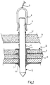
- Figure 1 is a cross section illustrating a PCB and a pin of known embodiment
- Figure 2 in cross section illustrates the PCB with the inventive pin
- Figure 3 in cross section illustrates a detail of the inventive pin
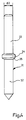
- Figure 4 is a side view of a further embodiment of a pin in accordance with the invention.
- FIG. 1 there is illustrated a known pin 1, by which an electrical conductor 2 is connected to electrical conductors 3 in a PCB 4.
- the latter is conventionally built up of insulating material layers 5 on which the conductors 3 are situated.
- the conductors 3 of the different layers 5 are connected to metal tabs 6 connected to each other via a metal tube 7 through the circuit board.
- This tube is achieved by a hole being drilled in the PCB 4 through the metal tabs 6, whereafter the inside of the hole is coated with metal.
- the electrical conductor 2 is connected to the pin 1 with the aid of a sliding contact 8, engaging against the pin 1 with the aid of spring bias.
- the pin 1 is retained in a holder 9 of plastic material, which also retains a plurality of unillustrated pins connected to the circuit board 4.
- the pin 1 is thrust into the tube 7, and to obtain good electrical and mechanical connection between the pin 1 and the tube 7 the pin is soldered in the tube by soldering metal 10.
- soldering metal 10 For soldering, the pin 1 is inserted in the tube, subsequent to which the inside of the tube 7 and the pin 1 are coated with flux, then the underside of the PCB 4 is lowered into a bath of molten soldering metal. During soldering the flux is heated and is forced away by the soldering metal 10 to creep along the surface of the pin 1 as indicated by arrows P in the figure. At the place of attachment of the pin in the holder 9, there are narrow gaps 12 between the pin 1 and the holder 9 through which the flux can creep.
- the flux can thus reach the surface 11, against which the gliding contact 8 is to engage, and cause contact resistance between the pin 1 and the contact 8. It has been found very difficult to form the holder 9 such that a completely sealed connection between the pin and holder is obtained, which would prevent the flux reaching the upper part of the pin.
- the PCB 4 with pin 21 in accordance with the invention are illustrated in Figure 2, and are formed such that they counteract the movement of the flux along the pin.
- the electrical conductors 2 are connected to the conductors 3 in the circuit board 4 via the pin 21, which is retained by the holder 9.
- the conductors 3 of the PCB are connected to metal tabs 22, which are mutually connnected right through the PCB 4 by metal tube 23.
- the pin 21 has a first elongate, uniformly thick part 24 which is thrust into the metal tube 23 and attached to it via soldering metal 25.
- the electrical conductors 2 are connected by gliding contacts 8, engaging against surfaces 29 of a second elongate, uniformly thick part 26 of the pin 21.
- the cross-sectional dimension d2 of the second part 26 is greater than the cross-sectional dimension d1 of the first part 24.
- the second part 26 projects out past the first part 24 round the entire periphery of the pin 21 so that a shoulder 27 is formed.
- the relationship between the cross-sectional dimensions d1 and d2 is less than 3:4 and the shoulder 27 has an extension in the longitudinal direction of the pin which is less than the difference between the cross-sectional dimensions.
- the shoulder 27 has sharp edges 30 which prevent the flux creeping, as will be explained below.
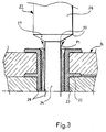
- FIG. 3 A fragmentary section of the pin 21 and PCB 4 is illustrated in Figure 3.
- the inside of the tube 23 and the first part 24 of the pin are coated with flux 28, which wets the surface of the first part 24 during soldering and creeps upwards as illustrated by the arrows P1. It has been found by trials that the creep of the flux is made more difficult by the edges 30 of the shoulder 27. During soldering there is a accumulation of flux at the lower one of the edges. When the amount of accumulated flux has reached a certain size the flux begins to creep along the surface of the shoulder 27 and a new accumulation of flux is formed at the upper one of the edges.
- the build-up of these accumulations of flux takes such a long time that there is time for soldering to be terminated and the termperature of the pin 21 to fall, so that the flux has time to solidify.
- the shoulder thus counteracts the creep of flux up around the second part 26 of the pin to the engaging surfaces 29 for the gliding contact 8.
- the shoulder 27 is situated spaced from the uppermost metal tab 22 and has no sealing function in co-action with it.
- a pin 31 has a first elongate, uniformly thick part 32 and a second elongate part 33 with a protuberance 34 extending round the entire periphery of the pin 31.
- the first part 32 is intended for thrusting into, and soldering to the hole in the PCB 4.
- the protuberance 34 forms a shoulder 35, which counteracts that the flux heated during soldering can creep up along the second part 33 of the pin 31, as described in connection with Figure 3.
- the spacing d3 between the pins is also standardized.
- this embodiment has the advantage that the diameter of the tab 22 is less than the diamter of the tab 6 for the known pin 1 according to Figure 1.
- pins have been thrust into holes in the PCB. It will be obvious to one skilled in the art that the invention can also be applied to pins which are soldered at the surface of a PCB.
Abstract
Description
- The invention relates to a pin attached to a printed circuit board (PCB) by soldering for connecting electrical conductors to the PCB, the pin having a first part soldered to a metal coating on the PCB, and a second part with which said electrical conductors can make contact, and where flux is used in soldering the pin, the flux wetting the surface of the pin and creeping away from the soldering location and the cross-sectional dimension of the second part of the pin is greater than the cross-sectional dimension of the fist part of the pin, whereby a shoulder is formed between the two parts.
- Pins are used in many applications for connecting electrical conductors to PCBs, the pins being soldered to the PCB. In soldering, a flux is used, which wets the pin and creeps along its surface. In such cases it is a known problem that during soldering the flux can creep to the upper part of the pin where there are the connected electrical conductors. The flux can there act chemically on an integrated circuit which is connected via the pin, for example, or constitute a contact resistance between the pin and a gliding contact thrust on to it. In order to prevent the flux from creeping along the pin it has been proposed to provide a tight closure round the pin, e.g. as described in the German patent application DE-A-3414343. In this publication there is described an insulating casing with pins for electrical connection, these pins being fixed in holes in the walls of the casing. Each pin has a transverse protuberance which is pressed into a corresponding hole in the casing. However, it has been found difficult to achieve a completely tight closure in this way, and it has been proposed to further seal the closure with the aid of glue or lacquer. A completely sealed closure has not been able to be provided with the aid of these sealing means either, and the flux has crept past the closure by capillary action.
- The problem described has been solved in accordance with the invention by a pin which is formed such that is counteracts the creep of the flux along the surface of the pin to the place of contact for the electrical conductors. The invention has the distinguishing features disclosed in the accompanying claims.
- An embodiment example of the present invention will now be described in more detail in connection with a drawing where Figure 1 is a cross section illustrating a PCB and a pin of known embodiment,
Figure 2 in cross section illustrates the PCB with the inventive pin,
Figure 3 in cross section illustrates a detail of the inventive pin, and
Figure 4 is a side view of a further embodiment of a pin in accordance with the invention. - In Figure 1 there is illustrated a known pin 1, by which an
electrical conductor 2 is connected toelectrical conductors 3 in a PCB 4. The latter is conventionally built up ofinsulating material layers 5 on which theconductors 3 are situated. Theconductors 3 of thedifferent layers 5 are connected tometal tabs 6 connected to each other via a metal tube 7 through the circuit board. This tube is achieved by a hole being drilled in the PCB 4 through themetal tabs 6, whereafter the inside of the hole is coated with metal. Theelectrical conductor 2 is connected to the pin 1 with the aid of a slidingcontact 8, engaging against the pin 1 with the aid of spring bias. The pin 1 is retained in aholder 9 of plastic material, which also retains a plurality of unillustrated pins connected to the circuit board 4. The pin 1 is thrust into the tube 7, and to obtain good electrical and mechanical connection between the pin 1 and the tube 7 the pin is soldered in the tube by solderingmetal 10. For soldering, the pin 1 is inserted in the tube, subsequent to which the inside of the tube 7 and the pin 1 are coated with flux, then the underside of the PCB 4 is lowered into a bath of molten soldering metal. During soldering the flux is heated and is forced away by the solderingmetal 10 to creep along the surface of the pin 1 as indicated by arrows P in the figure. At the place of attachment of the pin in theholder 9, there arenarrow gaps 12 between the pin 1 and theholder 9 through which the flux can creep. The flux can thus reach thesurface 11, against which thegliding contact 8 is to engage, and cause contact resistance between the pin 1 and thecontact 8. It has been found very difficult to form theholder 9 such that a completely sealed connection between the pin and holder is obtained, which would prevent the flux reaching the upper part of the pin. - The PCB 4 with
pin 21 in accordance with the invention are illustrated in Figure 2, and are formed such that they counteract the movement of the flux along the pin. Theelectrical conductors 2 are connected to theconductors 3 in the circuit board 4 via thepin 21, which is retained by theholder 9. As described in connection with Figure 1, theconductors 3 of the PCB are connected tometal tabs 22, which are mutually connnected right through the PCB 4 bymetal tube 23. Thepin 21 has a first elongate, uniformlythick part 24 which is thrust into themetal tube 23 and attached to it via solderingmetal 25. Theelectrical conductors 2 are connected bygliding contacts 8, engaging againstsurfaces 29 of a second elongate, uniformlythick part 26 of thepin 21. The cross-sectional dimension d2 of thesecond part 26 is greater than the cross-sectional dimension d1 of thefirst part 24. At the middle portion of thepin 21 thesecond part 26 projects out past thefirst part 24 round the entire periphery of thepin 21 so that ashoulder 27 is formed. The relationship between the cross-sectional dimensions d1 and d2 is less than 3:4 and theshoulder 27 has an extension in the longitudinal direction of the pin which is less than the difference between the cross-sectional dimensions. At the junctions between theshoulder 27 and theparts sharp edges 30 which prevent the flux creeping, as will be explained below. - A fragmentary section of the
pin 21 and PCB 4 is illustrated in Figure 3. The inside of thetube 23 and thefirst part 24 of the pin are coated withflux 28, which wets the surface of thefirst part 24 during soldering and creeps upwards as illustrated by the arrows P1. It has been found by trials that the creep of the flux is made more difficult by theedges 30 of theshoulder 27. During soldering there is a accumulation of flux at the lower one of the edges. When the amount of accumulated flux has reached a certain size the flux begins to creep along the surface of theshoulder 27 and a new accumulation of flux is formed at the upper one of the edges. The build-up of these accumulations of flux takes such a long time that there is time for soldering to be terminated and the termperature of thepin 21 to fall, so that the flux has time to solidify. The shoulder thus counteracts the creep of flux up around thesecond part 26 of the pin to theengaging surfaces 29 for thegliding contact 8. In the embodiment theshoulder 27 is situated spaced from theuppermost metal tab 22 and has no sealing function in co-action with it. By the shoulder being situated with this spacing from the tab, heat conduction during soldering is delayed to theupper part 26 of the thepin 21, and cooling the pin is facilitated. This contributes to the solidification of theflux 28 and prevention of the flux from creeping to thecontact surfaces 29. - An alternative embodiment of the
pin 21 described above is illustrated in Figure 4. Apin 31 has a first elongate, uniformlythick part 32 and a secondelongate part 33 with aprotuberance 34 extending round the entire periphery of thepin 31. Thefirst part 32 is intended for thrusting into, and soldering to the hole in the PCB 4. Theprotuberance 34 forms ashoulder 35, which counteracts that the flux heated during soldering can creep up along thesecond part 33 of thepin 31, as described in connection with Figure 3. - The
pins second parts gliding contacts 8. The spacing d3 between the pins is also standardized. According to an advantageous embodiment of the invention, the first, narrow part of thepin 21 in Figures 2 and 3 is rectangular, with the cross sectional dimension d1=0,3 mm, and with thesecond part 26 projecting outside thefirst part 24 along the entire periphery of the pin. Apart from the properties described above, this embodiment has the advantage that the diameter of thetab 22 is less than the diamter of thetab 6 for the known pin 1 according to Figure 1. This results in that the distance between the outer edges of thetabs 22 will be relatively great and a relatively large number ofconductors 3 on the PCB 4 can have room between the tabs. In turn this results in that the number oflayers 5 of the PCB 4 can be relatively small, which makes the PCB cheap. - In the embodiments described above the pins have been thrust into holes in the PCB. It will be obvious to one skilled in the art that the invention can also be applied to pins which are soldered at the surface of a PCB.
Claims (4)
- A pin (21;31) attached to a printed circuit board (PCB) (4) by soldering for connecting electrical conductors to the PCB (4), the pin having a first part (24;32) soldered to a metal coating (22) on the PCB, and a second part (26;34) with which said electrical conductors can make contact, and where flux is used in soldering the pin, the flux wetting the surface of the pin and creeping away from the soldering location and the cross-sectional dimension of the second part (26;34) of the pin (21;31) is greater than the cross-sectional dimension of the first part (24;32) of the pin (21;31), whereby a shoulder (27,35) is formed between the two parts (26,34; 24,32), the pin (21;31) having a junction with a sharp edge (30) between the shoulder (27;35) and at least one of the first (24;32) or second (26;34) parts of the pin (21;31), said edge (30) counteracting creep of the flux (28) along the surface of the second part (26;34) of the pin (21;31).
- Pin attached to a PCB by soldering as claimed in claim 1, whereby the shoulder (27;35) is situated spaced from the metal coating (22,23) of the PCB(4).
- Pin attached to a PCB by soldering as claimed in claim 1 or claim 2, whereby the shoulder (27;35) is extending around the entire periphery of the pin (21;31).
- Pin attached to a PCB by soldering as claimed in claim 1, 2 or 3 whereby the metal coating (22,23) includes a tube (23) passing through the PCB (4), and in that the first part (24;32) of the pin (21;31) is elongate, unliformly thick and projects into the tube (23).
Priority Applications (1)
| Application Number | Priority Date | Filing Date | Title |
|---|---|---|---|
| AT88905456T ATE103112T1 (en) | 1987-06-11 | 1988-05-18 | A NEEDLE SOLDERED TO AN INTEGRATED PRESSURE PLATE. |
Applications Claiming Priority (2)
| Application Number | Priority Date | Filing Date | Title |
|---|---|---|---|
| SE8702441A SE457838B (en) | 1987-06-11 | 1987-06-11 | STYLE WANTED TO BE FIXED BY A CIRCUIT THROUGH WELDING |
| SE8702441 | 1987-06-11 |
Publications (2)
| Publication Number | Publication Date |
|---|---|
| EP0321525A1 EP0321525A1 (en) | 1989-06-28 |
| EP0321525B1 true EP0321525B1 (en) | 1994-03-16 |
Family
ID=20368829
Family Applications (1)
| Application Number | Title | Priority Date | Filing Date |
|---|---|---|---|
| EP88905456A Expired - Lifetime EP0321525B1 (en) | 1987-06-11 | 1988-05-18 | A pin fastened to a printed circuit board by soldering |
Country Status (19)
| Country | Link |
|---|---|
| US (1) | US5000691A (en) |
| EP (1) | EP0321525B1 (en) |
| KR (1) | KR890702281A (en) |
| AU (1) | AU601060B2 (en) |
| BR (1) | BR8807087A (en) |
| DE (1) | DE3888488T2 (en) |
| DK (1) | DK163851C (en) |
| EG (1) | EG18423A (en) |
| ES (1) | ES2008536A6 (en) |
| FI (1) | FI93911C (en) |
| GR (1) | GR880100378A (en) |
| IE (1) | IE63145B1 (en) |
| MA (1) | MA21299A1 (en) |
| MX (1) | MX169273B (en) |
| MY (1) | MY103092A (en) |
| SE (1) | SE457838B (en) |
| TN (1) | TNSN88054A1 (en) |
| TR (1) | TR26976A (en) |
| WO (1) | WO1988010015A1 (en) |
Cited By (1)
| Publication number | Priority date | Publication date | Assignee | Title |
|---|---|---|---|---|
| US10798856B2 (en) * | 2015-12-03 | 2020-10-06 | Protosonic Limited | Apparatus for holding a printed circuit board |
Families Citing this family (10)
| Publication number | Priority date | Publication date | Assignee | Title |
|---|---|---|---|---|
| JP3426801B2 (en) * | 1995-08-15 | 2003-07-14 | 株式会社ミツバ | Electronic components |
| ES2140340B1 (en) * | 1998-03-13 | 2000-10-16 | Mecanismos Aux Es Ind S A M A | LASER WELDING PROCEDURE APPLICABLE TO THE JOINT OF PINS ON PRINTED CIRCUITS. |
| KR100319291B1 (en) | 1999-03-13 | 2002-01-09 | 윤종용 | Printed circuit board and soldering method of printed circuit board |
| US6798191B1 (en) | 1999-08-09 | 2004-09-28 | Power Measurement Ltd. | Revenue meter with a graphic user interface being operative to display scalable objects |
| US6186842B1 (en) * | 1999-08-09 | 2001-02-13 | Power Measurement Ltd. | Revenue meter bayonet assembly and method of attachment |
| CN100484371C (en) * | 2004-06-21 | 2009-04-29 | 鸿富锦精密工业(深圳)有限公司 | Welding disk for preventing host board short circuit |
| CN1735321A (en) * | 2004-08-11 | 2006-02-15 | 鸿富锦精密工业(深圳)有限公司 | Circuit board with improvement pad |
| US9674943B2 (en) * | 2012-12-06 | 2017-06-06 | Intel Corporation | Actuation mechanisms for electrical interconnections |
| TW201517716A (en) * | 2013-10-18 | 2015-05-01 | Delta Electronics Inc | Circuit board assembly and conductive wire fixing device and method thereof |
| US10886685B2 (en) * | 2019-03-08 | 2021-01-05 | Onanon, Inc. | Preformed solder-in-pin system |
Family Cites Families (7)
| Publication number | Priority date | Publication date | Assignee | Title |
|---|---|---|---|---|
| US3268653A (en) * | 1964-04-29 | 1966-08-23 | Ibm | Printed circuit board with solder resistant coating in the through-hole connectors |
| US3428934A (en) * | 1967-02-28 | 1969-02-18 | Amp Inc | Electrical connector for printed circuit board |
| US4236776A (en) * | 1978-08-24 | 1980-12-02 | Augat Inc. | Electrical contact with improved means for solder wicking and degassing |
| US4421368A (en) * | 1981-07-31 | 1983-12-20 | Western Electric Company, Inc. | Lead-receiving socket, multi-socket assembly incorporating same and method of effecting circuit interconnections therewith |
| US4577923A (en) * | 1983-03-24 | 1986-03-25 | Nec Corporation | Microwave integrated circuit and mounting device therefor |
| DE3414343A1 (en) * | 1984-04-16 | 1985-10-17 | Siemens AG, 1000 Berlin und 8000 München | Electrical plug connector |
| US4723925A (en) * | 1987-03-02 | 1988-02-09 | Woven Electronics Corporation | Crimp contact for a printed circuit board and method |
-
1987
- 1987-06-11 SE SE8702441A patent/SE457838B/en not_active IP Right Cessation
-
1988
- 1988-05-18 WO PCT/SE1988/000253 patent/WO1988010015A1/en active IP Right Grant
- 1988-05-18 DE DE3888488T patent/DE3888488T2/en not_active Expired - Fee Related
- 1988-05-18 AU AU19468/88A patent/AU601060B2/en not_active Ceased
- 1988-05-18 EP EP88905456A patent/EP0321525B1/en not_active Expired - Lifetime
- 1988-05-18 BR BR888807087A patent/BR8807087A/en not_active IP Right Cessation
- 1988-05-18 KR KR1019890700195A patent/KR890702281A/en not_active Application Discontinuation
- 1988-05-25 MX MX011633A patent/MX169273B/en unknown
- 1988-05-25 EG EG280/88A patent/EG18423A/en active
- 1988-05-30 IE IE161988A patent/IE63145B1/en not_active IP Right Cessation
- 1988-06-02 MY MYPI88000578A patent/MY103092A/en unknown
- 1988-06-03 TN TNTNSN88054A patent/TNSN88054A1/en unknown
- 1988-06-03 TR TR00392/88A patent/TR26976A/en unknown
- 1988-06-09 MA MA21542A patent/MA21299A1/en unknown
- 1988-06-10 ES ES8801803A patent/ES2008536A6/en not_active Expired
- 1988-06-13 GR GR880100378A patent/GR880100378A/en unknown
-
1989
- 1989-01-24 FI FI890345A patent/FI93911C/en not_active IP Right Cessation
- 1989-02-10 DK DK062789A patent/DK163851C/en not_active IP Right Cessation
-
1990
- 1990-03-12 US US07/492,326 patent/US5000691A/en not_active Expired - Lifetime
Cited By (1)
| Publication number | Priority date | Publication date | Assignee | Title |
|---|---|---|---|---|
| US10798856B2 (en) * | 2015-12-03 | 2020-10-06 | Protosonic Limited | Apparatus for holding a printed circuit board |
Also Published As
| Publication number | Publication date |
|---|---|
| MY103092A (en) | 1993-04-30 |
| EG18423A (en) | 1993-04-30 |
| BR8807087A (en) | 1989-10-31 |
| IE63145B1 (en) | 1995-03-22 |
| FI93911B (en) | 1995-02-28 |
| DK62789A (en) | 1989-02-10 |
| FI890345A0 (en) | 1989-01-24 |
| MA21299A1 (en) | 1988-12-31 |
| SE457838B (en) | 1989-01-30 |
| IE881619L (en) | 1988-12-11 |
| GR880100378A (en) | 1989-03-08 |
| TNSN88054A1 (en) | 1990-07-10 |
| FI93911C (en) | 1995-06-12 |
| US5000691A (en) | 1991-03-19 |
| TR26976A (en) | 1994-09-12 |
| DE3888488D1 (en) | 1994-04-21 |
| SE8702441L (en) | 1988-12-12 |
| AU601060B2 (en) | 1990-08-30 |
| ES2008536A6 (en) | 1989-07-16 |
| DK62789D0 (en) | 1989-02-10 |
| SE8702441D0 (en) | 1987-06-11 |
| FI890345A (en) | 1989-01-24 |
| DK163851B (en) | 1992-04-06 |
| KR890702281A (en) | 1989-12-23 |
| WO1988010015A1 (en) | 1988-12-15 |
| AU1946888A (en) | 1989-01-04 |
| EP0321525A1 (en) | 1989-06-28 |
| DE3888488T2 (en) | 1994-06-23 |
| MX169273B (en) | 1993-06-28 |
| DK163851C (en) | 1992-09-07 |
Similar Documents
| Publication | Publication Date | Title |
|---|---|---|
| US2707272A (en) | Mounting device for electric components | |
| US4230385A (en) | Printed circuit board, electrical connector and method of assembly | |
| US4109295A (en) | Solderless circuit board component | |
| EP0321525B1 (en) | A pin fastened to a printed circuit board by soldering | |
| EP0797379B1 (en) | Circuit board and process for mounting and soldering of electronic components in accurate positions on the surface of the circuit board | |
| US3754324A (en) | Solder resist | |
| US4216576A (en) | Printed circuit board, electrical connector and method of assembly | |
| US4900279A (en) | Solder terminal | |
| US3184532A (en) | Electrical component and method of assembly | |
| US4797110A (en) | Printed circuit board with integral electrical connector and method for making it using wave soldering | |
| US4723923A (en) | Low insertion, stamped and formed contact sleeve | |
| US4592137A (en) | Method of circuit connection across both surfaces of substrate | |
| US6146212A (en) | Terminal connector assembly | |
| US5589669A (en) | Electrical contact for printed circuit boards | |
| EP0548810B1 (en) | Stamped and formed sealed pin | |
| US5090926A (en) | Solderable lead | |
| US3780211A (en) | Insulating printed-circuit board having pin-shaped connecting members | |
| US4679870A (en) | Manufacture of low profile clip connector | |
| JPH09205264A (en) | Packaging board, its manufacturing method, and circuit board used for packaging board | |
| CA1052475A (en) | Double faced printed circuit board interconnection | |
| JPH07254775A (en) | Circuit board | |
| JPH0439878A (en) | Connector | |
| JPH0897530A (en) | Electronic part mounting board and its manufacture | |
| JP3153109B2 (en) | Electronic components | |
| JPH0529108U (en) | Surface mount component terminals |
Legal Events
| Date | Code | Title | Description |
|---|---|---|---|
| PUAI | Public reference made under article 153(3) epc to a published international application that has entered the european phase |
Free format text: ORIGINAL CODE: 0009012 |
|
| 17P | Request for examination filed |
Effective date: 19890113 |
|
| AK | Designated contracting states |
Kind code of ref document: A1 Designated state(s): AT CH DE FR GB IT LI NL |
|
| 17Q | First examination report despatched |
Effective date: 19920316 |
|
| GRAA | (expected) grant |
Free format text: ORIGINAL CODE: 0009210 |
|
| AK | Designated contracting states |
Kind code of ref document: B1 Designated state(s): AT CH DE FR GB IT LI NL |
|
| REF | Corresponds to: |
Ref document number: 103112 Country of ref document: AT Date of ref document: 19940415 Kind code of ref document: T |
|
| ITF | It: translation for a ep patent filed |
Owner name: FUMERO BREVETTI S.N.C. |
|
| REF | Corresponds to: |
Ref document number: 3888488 Country of ref document: DE Date of ref document: 19940421 |
|
| ET | Fr: translation filed | ||
| PLBE | No opposition filed within time limit |
Free format text: ORIGINAL CODE: 0009261 |
|
| STAA | Information on the status of an ep patent application or granted ep patent |
Free format text: STATUS: NO OPPOSITION FILED WITHIN TIME LIMIT |
|
| 26N | No opposition filed | ||
| PGFP | Annual fee paid to national office [announced via postgrant information from national office to epo] |
Ref country code: FR Payment date: 19990430 Year of fee payment: 12 |
|
| PGFP | Annual fee paid to national office [announced via postgrant information from national office to epo] |
Ref country code: DE Payment date: 19990503 Year of fee payment: 12 Ref country code: AT Payment date: 19990503 Year of fee payment: 12 |
|
| PGFP | Annual fee paid to national office [announced via postgrant information from national office to epo] |
Ref country code: GB Payment date: 19990504 Year of fee payment: 12 |
|
| PGFP | Annual fee paid to national office [announced via postgrant information from national office to epo] |
Ref country code: CH Payment date: 19990505 Year of fee payment: 12 |
|
| PGFP | Annual fee paid to national office [announced via postgrant information from national office to epo] |
Ref country code: NL Payment date: 19990510 Year of fee payment: 12 |
|
| PG25 | Lapsed in a contracting state [announced via postgrant information from national office to epo] |
Ref country code: GB Free format text: LAPSE BECAUSE OF NON-PAYMENT OF DUE FEES Effective date: 20000518 Ref country code: AT Free format text: LAPSE BECAUSE OF NON-PAYMENT OF DUE FEES Effective date: 20000518 |
|
| PG25 | Lapsed in a contracting state [announced via postgrant information from national office to epo] |
Ref country code: LI Free format text: LAPSE BECAUSE OF NON-PAYMENT OF DUE FEES Effective date: 20000531 Ref country code: CH Free format text: LAPSE BECAUSE OF NON-PAYMENT OF DUE FEES Effective date: 20000531 |
|
| PG25 | Lapsed in a contracting state [announced via postgrant information from national office to epo] |
Ref country code: NL Free format text: LAPSE BECAUSE OF NON-PAYMENT OF DUE FEES Effective date: 20001201 |
|
| GBPC | Gb: european patent ceased through non-payment of renewal fee |
Effective date: 20000518 |
|
| REG | Reference to a national code |
Ref country code: CH Ref legal event code: PL |
|
| PG25 | Lapsed in a contracting state [announced via postgrant information from national office to epo] |
Ref country code: FR Free format text: LAPSE BECAUSE OF NON-PAYMENT OF DUE FEES Effective date: 20010131 |
|
| NLV4 | Nl: lapsed or anulled due to non-payment of the annual fee |
Effective date: 20001201 |
|
| PG25 | Lapsed in a contracting state [announced via postgrant information from national office to epo] |
Ref country code: DE Free format text: LAPSE BECAUSE OF NON-PAYMENT OF DUE FEES Effective date: 20010301 |
|
| REG | Reference to a national code |
Ref country code: FR Ref legal event code: ST |
|
| PG25 | Lapsed in a contracting state [announced via postgrant information from national office to epo] |
Ref country code: IT Free format text: LAPSE BECAUSE OF NON-PAYMENT OF DUE FEES;WARNING: LAPSES OF ITALIAN PATENTS WITH EFFECTIVE DATE BEFORE 2007 MAY HAVE OCCURRED AT ANY TIME BEFORE 2007. THE CORRECT EFFECTIVE DATE MAY BE DIFFERENT FROM THE ONE RECORDED. Effective date: 20050518 |