EP0321312B1 - A circuit for removing crosstalk components in a carrier chrominance signal - Google Patents
A circuit for removing crosstalk components in a carrier chrominance signal Download PDFInfo
- Publication number
- EP0321312B1 EP0321312B1 EP88312021A EP88312021A EP0321312B1 EP 0321312 B1 EP0321312 B1 EP 0321312B1 EP 88312021 A EP88312021 A EP 88312021A EP 88312021 A EP88312021 A EP 88312021A EP 0321312 B1 EP0321312 B1 EP 0321312B1
- Authority
- EP
- European Patent Office
- Prior art keywords
- signal
- circuit
- delay
- chrominance
- circuit means
- Prior art date
- Legal status (The legal status is an assumption and is not a legal conclusion. Google has not performed a legal analysis and makes no representation as to the accuracy of the status listed.)
- Expired
Links
Images


Classifications
-
- H—ELECTRICITY
- H04—ELECTRIC COMMUNICATION TECHNIQUE
- H04N—PICTORIAL COMMUNICATION, e.g. TELEVISION
- H04N9/00—Details of colour television systems
- H04N9/79—Processing of colour television signals in connection with recording
- H04N9/7908—Suppression of interfering signals at the reproducing side, e.g. noise
- H04N9/7917—Suppression of interfering signals at the reproducing side, e.g. noise the interfering signals being cross-talk signals
-
- H—ELECTRICITY
- H04—ELECTRIC COMMUNICATION TECHNIQUE
- H04N—PICTORIAL COMMUNICATION, e.g. TELEVISION
- H04N9/00—Details of colour television systems
- H04N9/64—Circuits for processing colour signals
- H04N9/646—Circuits for processing colour signals for image enhancement, e.g. vertical detail restoration, cross-colour elimination, contour correction, chrominance trapping filters
-
- H—ELECTRICITY
- H04—ELECTRIC COMMUNICATION TECHNIQUE
- H04N—PICTORIAL COMMUNICATION, e.g. TELEVISION
- H04N9/00—Details of colour television systems
- H04N9/79—Processing of colour television signals in connection with recording
- H04N9/80—Transformation of the television signal for recording, e.g. modulation, frequency changing; Inverse transformation for playback
- H04N9/82—Transformation of the television signal for recording, e.g. modulation, frequency changing; Inverse transformation for playback the individual colour picture signal components being recorded simultaneously only
- H04N9/83—Transformation of the television signal for recording, e.g. modulation, frequency changing; Inverse transformation for playback the individual colour picture signal components being recorded simultaneously only the recorded chrominance signal occupying a frequency band under the frequency band of the recorded brightness signal
- H04N9/84—Transformation of the television signal for recording, e.g. modulation, frequency changing; Inverse transformation for playback the individual colour picture signal components being recorded simultaneously only the recorded chrominance signal occupying a frequency band under the frequency band of the recorded brightness signal the recorded signal showing a feature, which is different in adjacent track parts, e.g. different phase or frequency
Definitions
- This invention relates generally to a chrominance signal processing circuit for a color video signal reproducing apparatus such as a VTR, and particularly to a circuit for removing crosstalk components in a carrier chrominance signal.
- a luminance signal and a chrominance signal are separated from a color video signal thereof, and the frequency of the chrominance signal is down-converted to obtain a frequency down-converted chrominance signal when the color video signal is recorded on a tape.
- the opposite signal-processings are performed to obtain a reproducing color video signal.
- a phase-shift processing method which is disclosed in Japanese Patent Publication No. 56-9073 is used, for example.
- colour-blurring occurs.
- EP-A-0,218,241 discloses a 3 line type comb filter similar to that of the present invention, however no provision is made to correct distortion introduced as a result of time delays in the various elements of the filter.
- the present invention has been developed in order to reduce the above-described drawbacks inherent to the known chrominance signal processing circuit.
- an object of the present invention to provide a new and useful chrominance signal processing circuit in which colour-blurring on a display can be reduced.
- circuit for removing crosstalk components from a chrominance carrier signal comprising:
- first delay circuit means adapted to delay said chrominance carrier signal
- inverter means adapted to invert the output signal from said first delay circuit means
- first higher-voltage detecting circuit means responsive to said chrominance carrier signal and the output signal from said inverter means for outputting a first higher-voltage signal corresponding to the higher of those signals;
- second delay circuit means adapted to delay said output signal from said first delay circuit means
- second higher-voltage detecting circuit means responsive to said output signal from said inverter means and an output signal from said second delay circuit means for outputting a second higher-voltage signal corresponding to the higher of those signals;
- first lower-voltage detecting circuit means responsive to said first and second higher-voltage signals for outputting a first lower-voltage signal corresponding to the lower of those signals
- second lower-voltage detecting circuit means responsive to said chrominance carrier signal and said output signal from said inverter means for outputting a second lower-voltage signal corresponding to the lower of those signals;
- third lower-voltage detecting circuit means responsive to said output signal from said inverter means and said output signal from said second delay circuit means for outputting a third lower-voltage signal corresponding to the lower of those signals;
- third higher-voltage detecting circuit means responsive to said second and third lower-voltage signals for outputting a third higher-voltage signal corresponding to the higher of those signals
- first adder means adapted to add said third higher-voltage signal and said first lower-voltage signal thereby producing a crosstalk-removed carrier chrominance signal
- second adder means adapted to add said chrominance carrier signal and said output from said inverter circuit, said first delay circuit means, said inverter means, and said adder means forming a comb filter adapted to correct a time delay due to the remainder of the circuit.
- a circuit for removing crosstalk components from a chrominance carrier signal comprising:
- a first delay circuit means adapted to delay said carrier chrominance signal
- a first 1/4 attenuation circuit adapted to attenuate said carrier chrominance signal by a factor of 4;
- an inverter means adapted to invert the output signal from said first delay circuit means
- second delay circuit means adapted to delay said output signal from said first delay circuit means
- a second 1/4 attenuation circuit means adapted to attenuate the output signal from said second delay circuit means by a factor of 4;
- a 1/2 attenuation circuit means adapted to attenuate the output signal from said inverter means by a factor of 2;
- first adder means adapted to add the output signals from said first and second 1/4 attenuation circuit means and the output signal from said 1/2 attenuation circuit means thereby producing a crosstalk-removed chrominance carrier signal
- a second adder means adapted to add said chrominance carrier signal and said output from said inverter means
- said first delay circuit means, said inverter means, said adder means forming a comb filter adapted to correct a time delay due to the remainder of the circuit.
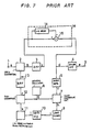
- the conventional chrominance signal processing circuit generally comprises a main converter 2, a first band-pass filter (BPF) 3, a two-line type chrominance signal comb filter 16, a killer circuit 4, a burst gate 6, a phase comparing circuit 7, a crystal oscillator 8, a loop filter 9, a 160 fH voltage controlled oscillator (VCO) 10, a 1/4 frequency-dividing and phase-shifting circuit 11, a sub-converter 12, and a second BPF 13.
- the two-line type chrominance signal comb filter 16 includes a 1-H delay circuit 14 and a subtractor 15.
- a reproduced frequency down-converted chrominance signal (a) is fed, via an input terminal 1, to the main converter 2.
- the chrominance signal (a) is converted to a carrier chrominance signal (b) having a frequency of 3.58 MHz, and then, the carrier chrominance signal (b) is sent to the first BPF 3.
- the first BPF 3 undesired band-width components are removed from the carrier chrominance signal (b).
- An outputted carrier chrominance signal (c) from the first BPF 3 is inputted into the chrominance signal comb filter 16 so as to be removed crosstalk components therefrom.
- Such a crosstalk-removed signal (d) is outputted, via the killer circuit 4, from the output terminal 5 as a reproduced chrominance signal (e).
- the crosstalk-removed signal (d) is also fed to the burst gate 6 for producing a burst signal (f).
- the burst signal (f) outputted from the burst gate 6 is inputted into the phase comparing circuit 7.
- a reference signal (g) having a frequency of 3.58 MHz is produced by the crystal oscillator 8, and is sent to the phase comparing circuit 7.
- a phase difference signal (h) is produced with the burst signal (f) being compared with the reference signal (g).
- the phase difference signal (h) is inputted into the loop filter 9 to be cut undesired frequency components.
- An outputted signal (i) from the loop filter 9 is sent to the 160 fH VCO 10 to be operated as a control voltage thereof, and the 160 fH VCO 10 outputs a 160 fH signal (j).
- the 160 fH signal (j) is frequency-divided and phase-shifted by the 1/4 frequency-dividing and phase-shifting circuit 11 to obtain a signal (k) of frequency 40 fH.
- This signal (k) and the reference signal (g) outputted from the crystal oscillator 8 are applied to the sub-converter 12 to produce a signal (l) having a frequency of 4.21 MHz.
- This signal (l) of 4.21 MHz is sent, via the second BPF 13, to the main converter 2 as a signal (m).
- Fig. 7 is of the NTSC system
- the 160 fH VCO 10 is changed into a 321 fH VCO
- the 1/4 frequency-dividing circuit 11 is changed into a 1/8 frequency-dividing circuit.
- the 1-H delay cirucit 14 is changed into a 2-H delay circuit.
- the chrominance signal is converted into a signal having a frequency of 4.43 MHz
- the crystal oscillator produces a signal having a frequency of 4.43 MHz thereby obtaining a 5.06 MHz signal from the second BPF.
- a reproduced image has a color-blurring portion (iii) in one line just below the upper red portion (i) as shown in Fig. 8B because there is no vertical-correlation between the upper red portion (i) and the lower colorless portion (ii).
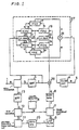
- Fig. 1 shows a block diagram of a chrominance signal processing circuit having a circuit for removing crosstalk components in the NTSC system according to a first embodiment of the present invention.
- the chrominance signal processing circuit of Fig. 1 is substantially the same as that of Fig. 7 except for a chrominance signal comb filter 27, and an adder 28.
- those parts which are the same as those of Fig. 7 are designated at the same numerals and description thereof is omitted.
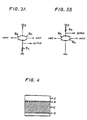
- the three-line type comb filter 27 includes first and second 1-H delay circuits 20 and 22, an inverter 21, first, second, and third higher-voltage detecting circuits (MAX cirucits) 18, 19 and 25, first, second, and third lower-voltage detecting circuits (MIN circuits) 23, 24, and 17, and an adder 26.
- MAX cirucits first, second, and third higher-voltage detecting circuits
- MIN circuits lower-voltage detecting circuits
- adder 26 the structure of these MAX circuits 18, 19, and 25 includes transistors Q1 and Q2 and a resistor R1 as shown in Fig. 3A
- the same of these MIN ciruicts includes transistors Q3 and Q4 and a resistor R2 as shown in Fig. 3B.
- Carrier chrominance signal (c) from first BPF 3 is fed to the first 1-H delay circuit 20, the first MAX circuit 18, and the first MIN circuit 23 in the three-line type comb filter 27.
- a delayed signal (n) outputted from the first 1-H delay circuit 20 is fed to the inverter 21 and the second 1-H delay circuit 22.
- An inverted signal (p) from the inverter 21 is sent to the first MAX circuit 18, the first MIN circuit 23, the second MAX circuit 19, and the second MIN circuit 24.
- a first higher voltage signal (s) between the carrier chrominance signal (c) and the inverted signal (p) is produced, and then the first higher voltage signal (s) is sent to the third MIN circucit 17.
- a first lower voltage signal (v) between the carrier chrominance signal (c) and the inverted signal (p) is produced, and then the first lower voltage signal (v) is sent to the third MAX circucit 25.
- a delayed signal (o) outputted from the second 1-H delay circuit 22 is also inputted into the second MAX circuit 19 and the second MIN circuit 24.
- the second MAX circuit 19 a second higher voltage signal (t) between the inverted signal (p) and the delayed signal (o) is produced, and then the second higher voltage signal (t) is fed to the third MIN cirucit 17.
- the second MIN circuit 24 a second lower voltage signal (w) between the inverted signal (p) and the delayed signal (o) is produced, and then the second lower voltage signal (w) is fed to the third MAX cirucit 25.
- a third lower voltage signal (u) between the first higher voltage signal (s) and the second higher voltage signal (t) is produced, and then the third lower voltage signal (u) is supplied to the adder 26.
- a third higher voltage signal (x) between the first lower voltage signal (v) and the second lower voltage signal (w) is produced, and then the third higher voltage signal (x) is supplied to the adder 26.
- An added signal (r) from the adder 26 is fed to killer circuit 4.
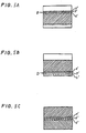
- the three-line comb filter 27 as a circuit for removing color-blurring and crosstalk component in a carrier chrominance signal will be described hereinbelow. It is assumed that a source image shown in Fig. 4 is applied in the three-line type comb filter 27. This image formed of an upper colorless portion (A), a middle colored portion (C), and a lower colorless portion (E). A numeral (B) denotes the first line of the middle colored portion (C) and a numeral (D) shows the first line of the lower colorless portion (E).
- each waveform of the signals (c), (p), (o), (s), (t), (u), (v), (w), (x), and (r) are shown in Fig. 6B.
- the signal (r) it can be understood that any chrominance signal is not outputted.
- all the signals (c), (p), (o), (s), (t), (u), (v), (w), (x), and (r) become equal as shown in Fig. 6C.
- the signal (r) is also of colorlessness.
- magenta and green when a hue is reversed between magenta and green as shown in Fig. 5C, i.e. when the signal (o′) is magenta and both the signals (p′) and (c′) are green, each waveform of the signals (c), (p), (o), (s), (t), (u), (v), (w), (x), and (r) are shown in Fig. 6D. It is to be noted that magenta and green can be completely distinguished.
- the signal (r) is outputted therefrom as an average signal between the signal (p) and one closer signal to the signal (p) in the signals (c) and (o), whereby the signal (p) is the main signal therebetween.
- the signal (p) shows a 1-H delayed signal.
- the adder 28 is required for removing the 1-H time duration as one part of a two-line type comb filter.
- the adder 28, the inverter 21, and the 1-H delay cirucit 20 form the two-line type comb filter for correcting such a time delay due to the three-line type comb filter 27.
- the signal (c) is added to the signal (p) to produce a signal (q), and the signal (q) is sent to the burst gate 6.
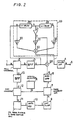
- Fig. 2 shows a block diagram of a chrominance signal processing circuit having a circuit for removing crosstalk components in the NTSC system according to a second embodiment of the present invention.
- the chrominance signal processing circuit of Fig. 2 is substantially the same as that of Fig. 1 except for a chrominance signal comb filter 29.
- those parts which are the same as those of Fig. 7 are designated at the same numerals and description thereof is omitted.
- the three-line type comb filter 29 includes first and second 1-H delay circuits 20 and 22, an inverter 21, first and second 1/4 attenuation circuits 30 and 32, a 1/2 attenuation circuit 31, and an adder 33.
- Carrier chrominance signal (c) from first BPF 3 is fed to the first 1-H delay circuit 20 and the first 1/4 attenuation circuit 30.
- An output signal (n) from the first 1-H delay circuit 20 is sent to the second 1-H delay circuit 22 and the inverter 21.
- an output signal (o) from the second 1-H delay circuit 22 is supplied to the second 1/4 attenuation circuit 32, and an output signal (p) from the inverter 21 is inputted into the 1/2 attenuation circuit 31.
- ouptut signals from the first and second 1/4 attenuation circuit 30 and 32 and the 1/2 attenuation circuit 31 are combined in the adder 33, and then the added signal (r′) is sent to the killer cirucit 4.
- Figs. 1 and 2 are of the NTSC system, when the above-mentioned present embodiments are applied to that of the PAL system, the following changes are required.
- the 160 fH VCO 10 is changed into a 321 fH VCO, and the 1/4 frequency-dividing and phase-shifting circuit 11 is changed into a 1/8 frequency-dividing and phase-shifting circuit.
- the first and second 1-H delay cirucits 20 and 22 are respectively changed into 2-H delay circuits.
- the chrominance signal is converted into a signal having a frequency of 4.43 MHz, and the crystal oscillator produces a signal having a frequency of 4.43 MHz thereby obtaining a 5.06 MHz signal from the second BPF 13.
Landscapes
- Engineering & Computer Science (AREA)
- Multimedia (AREA)
- Signal Processing (AREA)
- Processing Of Color Television Signals (AREA)
Description
- This invention relates generally to a chrominance signal processing circuit for a color video signal reproducing apparatus such as a VTR, and particularly to a circuit for removing crosstalk components in a carrier chrominance signal.
- In general VTRs used at the present time, a luminance signal and a chrominance signal are separated from a color video signal thereof, and the frequency of the chrominance signal is down-converted to obtain a frequency down-converted chrominance signal when the color video signal is recorded on a tape. When such recorded color video signal is reproduced, the opposite signal-processings are performed to obtain a reproducing color video signal. Meanwhile, in order to reduce crosstalk components of the reproducing down-converted chrominance signal on the tape, a phase-shift processing method which is disclosed in Japanese Patent Publication No. 56-9073 is used, for example. However, when there is no vertical-correlation between adjacent horizontal lines on a displayed image, colour-blurring occurs.
- "Flicker-Free non-interlaced Receiving System for standard colour TV signals" IEEE Transactions on Consumer Electronics CE-31
No 3 August 1985 p.p. 240-253 discloses a two line logical comb filter similar to that of the present invention, however no provision is made for the correction of time delays introduced by the various logical elements. - EP-A-0,218,241 (Faroudja Laboratories Inc) discloses a 3 line type comb filter similar to that of the present invention, however no provision is made to correct distortion introduced as a result of time delays in the various elements of the filter.
- The present invention has been developed in order to reduce the above-described drawbacks inherent to the known chrominance signal processing circuit.
- It is, therefore, an object of the present invention to provide a new and useful chrominance signal processing circuit in which colour-blurring on a display can be reduced.
- It is another object of the invention to provide a chrominance signal processing circuit in which crosstalk components in a carrier chrominance signal can be effectively reduced.
- In accordance with the present invention there is a circuit for removing crosstalk components from a chrominance carrier signal, the circuit comprising:
- first delay circuit means adapted to delay said chrominance carrier signal;
- inverter means adapted to invert the output signal from said first delay circuit means;
- first higher-voltage detecting circuit means responsive to said chrominance carrier signal and the output signal from said inverter means for outputting a first higher-voltage signal corresponding to the higher of those signals;
- second delay circuit means adapted to delay said output signal from said first delay circuit means;
- second higher-voltage detecting circuit means responsive to said output signal from said inverter means and an output signal from said second delay circuit means for outputting a second higher-voltage signal corresponding to the higher of those signals;
- first lower-voltage detecting circuit means responsive to said first and second higher-voltage signals for outputting a first lower-voltage signal corresponding to the lower of those signals;
- second lower-voltage detecting circuit means responsive to said chrominance carrier signal and said output signal from said inverter means for outputting a second lower-voltage signal corresponding to the lower of those signals;
- third lower-voltage detecting circuit means responsive to said output signal from said inverter means and said output signal from said second delay circuit means for outputting a third lower-voltage signal corresponding to the lower of those signals;
- third higher-voltage detecting circuit means responsive to said second and third lower-voltage signals for outputting a third higher-voltage signal corresponding to the higher of those signals;
- first adder means adapted to add said third higher-voltage signal and said first lower-voltage signal thereby producing a crosstalk-removed carrier chrominance signal; and
- second adder means adapted to add said chrominance carrier signal and said output from said inverter circuit, said first delay circuit means, said inverter means, and said adder means forming a comb filter adapted to correct a time delay due to the remainder of the circuit.
- In accordance with a further aspect of the present invention there is provided a circuit for removing crosstalk components from a chrominance carrier signal, comprising:
- a first delay circuit means adapted to delay said carrier chrominance signal;
- a first 1/4 attenuation circuit adapted to attenuate said carrier chrominance signal by a factor of 4;
- an inverter means adapted to invert the output signal from said first delay circuit means;
- second delay circuit means adapted to delay said output signal from said first delay circuit means;
- a second 1/4 attenuation circuit means adapted to attenuate the output signal from said second delay circuit means by a factor of 4;
- a 1/2 attenuation circuit means adapted to attenuate the output signal from said inverter means by a factor of 2;
- first adder means adapted to add the output signals from said first and second 1/4 attenuation circuit means and the output signal from said 1/2 attenuation circuit means thereby producing a crosstalk-removed chrominance carrier signal, and
- a second adder means adapted to add said chrominance carrier signal and said output from said inverter means;
- said first delay circuit means, said inverter means, said adder means forming a comb filter adapted to correct a time delay due to the remainder of the circuit.
- The object and features of the present invention will become more readily apparent from the following detailed description of the preferred embodiments taken in conjunction with the accompanying drawings in which:
- Fig. 1 is a block diagram of a chrominance signal processing circuit having a circuit for removing crosstalk components in a carrier chrominance signal according to a first embodiment of the present invention;
- Fig. 2 is a block diagram of a chrominance signal processing circuit having a circuit for removing crosstalk components in a carrier chrominance signal according to a second embodiment of the invention;
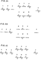
- Fig. 3A is a higher-voltage detecting circuit used in the circuit for removing crosstalk components in a carrier chrominance signal;
- Fig. 3B is a lower-voltage detecting circuit used in the circuit for removing crosstalk components in a carrier chrominance signal;
- Fig. 4 is one example of source images which is to be inputted into the chrominance signal processing circuit of Fig. 1;
- Figs. 5A, 5B, and 5C are image patterns for describing the operation of the circuit for removing crosstalk components in a carrier chrominance signal;
- Figs. 6A, 6B, 6C, 6D, and 6E are waveforms for describing the operation of the circuit for removing crosstalk components in a carrier chrominance signal;
- Fig. 7 is a block diagram of a conventional chrominance signal processing circuit;
- Fig. 8A is one example of source images; and
- Fig. 8B is a reproduced image obtained by supplying the source image of Fig. 8A to the conventional chrominance signal processing circuit.
- The same or corresponding elements and parts are designated at like reference numerals throughout the drawings.
- Prior to describing the preferred embodiments of the present invention, the above-mentioned conventional chrominance signal processing circuit in the NTSC system will be described for a better understanding of the present invention.
- Referring now to Fig. 7, the conventional chrominance signal processing circuit generally comprises a
main converter 2, a first band-pass filter (BPF) 3, a two-line type chrominance signal comb filter 16, akiller circuit 4, aburst gate 6, aphase comparing circuit 7, acrystal oscillator 8, a loop filter 9, a 160 fH voltage controlled oscillator (VCO) 10, a 1/4 frequency-dividing and phase-shiftingcircuit 11, asub-converter 12, and asecond BPF 13. The two-line type chrominance signal comb filter 16 includes a 1-H delay circuit 14 and asubtractor 15. - The operation of the conventional chrominance signal processing circuit having the above-mentioned structure will be described hereinbelow. A reproduced frequency down-converted chrominance signal (a) is fed, via an
input terminal 1, to themain converter 2. In themain converter 2, the chrominance signal (a) is converted to a carrier chrominance signal (b) having a frequency of 3.58 MHz, and then, the carrier chrominance signal (b) is sent to thefirst BPF 3. In thefirst BPF 3, undesired band-width components are removed from the carrier chrominance signal (b). An outputted carrier chrominance signal (c) from thefirst BPF 3 is inputted into the chrominance signal comb filter 16 so as to be removed crosstalk components therefrom. Such a crosstalk-removed signal (d) is outputted, via thekiller circuit 4, from theoutput terminal 5 as a reproduced chrominance signal (e). The crosstalk-removed signal (d) is also fed to theburst gate 6 for producing a burst signal (f). The burst signal (f) outputted from theburst gate 6 is inputted into thephase comparing circuit 7. - Meanwhile, a reference signal (g) having a frequency of 3.58 MHz is produced by the
crystal oscillator 8, and is sent to thephase comparing circuit 7. In thephase comparing circuit 7, a phase difference signal (h) is produced with the burst signal (f) being compared with the reference signal (g). The phase difference signal (h) is inputted into the loop filter 9 to be cut undesired frequency components. An outputted signal (i) from the loop filter 9 is sent to the160 fH VCO 10 to be operated as a control voltage thereof, and the160 fH VCO 10 outputs a 160 fH signal (j). The 160 fH signal (j) is frequency-divided and phase-shifted by the 1/4 frequency-dividing and phase-shiftingcircuit 11 to obtain a signal (k) of frequency 40 fH. This signal (k) and the reference signal (g) outputted from thecrystal oscillator 8 are applied to the sub-converter 12 to produce a signal (ℓ) having a frequency of 4.21 MHz. This signal (ℓ) of 4.21 MHz is sent, via thesecond BPF 13, to themain converter 2 as a signal (m). - Although the block diagram of Fig. 7 is of the NTSC system, when the above-mentioned conventional circuit is applied to the PAL system, the following changes are required. The 160
fH VCO 10 is changed into a 321 fH VCO, and the 1/4 frequency-dividingcircuit 11 is changed into a 1/8 frequency-dividing circuit. Besides, the 1-H delay cirucit 14 is changed into a 2-H delay circuit. Here, in the main converter, the chrominance signal is converted into a signal having a frequency of 4.43 MHz, and the crystal oscillator produces a signal having a frequency of 4.43 MHz thereby obtaining a 5.06 MHz signal from the second BPF. - In the above-mentioned conventional chrominance signal processing circuit, however, assuming that a source image is formed of an upper red portion (i) and a lower colorless portion (ii) as shown in Fig. 8A, a reproduced image has a color-blurring portion (iii) in one line just below the upper red portion (i) as shown in Fig. 8B because there is no vertical-correlation between the upper red portion (i) and the lower colorless portion (ii).
- Fig. 1 shows a block diagram of a chrominance signal processing circuit having a circuit for removing crosstalk components in the NTSC system according to a first embodiment of the present invention. The chrominance signal processing circuit of Fig. 1 is substantially the same as that of Fig. 7 except for a chrominance
signal comb filter 27, and anadder 28. In this diagram, those parts which are the same as those of Fig. 7 are designated at the same numerals and description thereof is omitted. - The three-line
type comb filter 27 includes first and second 1-H delay circuits inverter 21, first, second, and third higher-voltage detecting circuits (MAX cirucits) 18, 19 and 25, first, second, and third lower-voltage detecting circuits (MIN circuits) 23, 24, and 17, and anadder 26. For example, the structure of theseMAX circuits - The operation of the three-line
type comb filter 27 will be described hereinbelow. Carrier chrominance signal (c) fromfirst BPF 3 is fed to the first 1-H delay circuit 20, thefirst MAX circuit 18, and thefirst MIN circuit 23 in the three-linetype comb filter 27. A delayed signal (n) outputted from the first 1-H delay circuit 20 is fed to theinverter 21 and the second 1-H delay circuit 22. An inverted signal (p) from theinverter 21 is sent to thefirst MAX circuit 18, thefirst MIN circuit 23, thesecond MAX circuit 19, and thesecond MIN circuit 24. In thefirst MAX circuit 18, a first higher voltage signal (s) between the carrier chrominance signal (c) and the inverted signal (p) is produced, and then the first higher voltage signal (s) is sent to thethird MIN circucit 17. In thefirst MIN circuit 23, a first lower voltage signal (v) between the carrier chrominance signal (c) and the inverted signal (p) is produced, and then the first lower voltage signal (v) is sent to thethird MAX circucit 25. - Meanwhile, a delayed signal (o) outputted from the second 1-
H delay circuit 22 is also inputted into thesecond MAX circuit 19 and thesecond MIN circuit 24. In thesecond MAX circuit 19, a second higher voltage signal (t) between the inverted signal (p) and the delayed signal (o) is produced, and then the second higher voltage signal (t) is fed to thethird MIN cirucit 17. In thesecond MIN circuit 24, a second lower voltage signal (w) between the inverted signal (p) and the delayed signal (o) is produced, and then the second lower voltage signal (w) is fed to thethird MAX cirucit 25. - Furthermore, in the
third MIN circuit 17, a third lower voltage signal (u) between the first higher voltage signal (s) and the second higher voltage signal (t) is produced, and then the third lower voltage signal (u) is supplied to theadder 26. In thethird MAX circuit 25, a third higher voltage signal (x) between the first lower voltage signal (v) and the second lower voltage signal (w) is produced, and then the third higher voltage signal (x) is supplied to theadder 26. An added signal (r) from theadder 26 is fed tokiller circuit 4. - Now, the three-
line comb filter 27 as a circuit for removing color-blurring and crosstalk component in a carrier chrominance signal will be described hereinbelow. It is assumed that a source image shown in Fig. 4 is applied in the three-linetype comb filter 27. This image formed of an upper colorless portion (A), a middle colored portion (C), and a lower colorless portion (E). A numeral (B) denotes the first line of the middle colored portion (C) and a numeral (D) shows the first line of the lower colorless portion (E). - When a signal corresponding to the portion (B) is outputted from the 1-
H delay circuit 20, signals (c′), (p′), and (o′) which are sequential on a display as horizontal lines are displayed as shown in Fig. 5A. In this case, each waveform of the signals (c), (p), (o), (s), (t), (u), (v), (w), (x), and (r) without crosstalk are shown in Fig. 6A. When a signal corresponding to the portion (D) is outputted from the 1-H delay circuit 20, the signals (c′), (p′), and (o′) are displayed as shown in Fig. 5B. In this case, each waveform of the signals (c), (p), (o), (s), (t), (u), (v), (w), (x), and (r) are shown in Fig. 6B. Thus, in the signal (r), it can be understood that any chrominance signal is not outputted. When these sequential signals (c′), (p′), and (o′) have the same color, since these three signals have vertical-correlation, all the signals (c), (p), (o), (s), (t), (u), (v), (w), (x), and (r) become equal as shown in Fig. 6C. When all sequential three signals (c′), (p′), and (o′) have no color, since these three signals have also vertical-correlation, the signal (r) is also of colorlessness. - Besides, when a hue is reversed between magenta and green as shown in Fig. 5C, i.e. when the signal (o′) is magenta and both the signals (p′) and (c′) are green, each waveform of the signals (c), (p), (o), (s), (t), (u), (v), (w), (x), and (r) are shown in Fig. 6D. It is to be noted that magenta and green can be completely distinguished.
- In the case of the crosstalk components, since the crosstalk signal has the same phase in every other horizontal line, each waveform of the signals (c), (p), (o), (s), (t), (u), (v), (w), (x), and (r) are shown in Fig. 6E. Thus, in the signal (r), it can be understood that such crosstalk components are substantially removed.
- As will be understood from the above description, in the three-line
type comb filter 27, the signal (r) is outputted therefrom as an average signal between the signal (p) and one closer signal to the signal (p) in the signals (c) and (o), whereby the signal (p) is the main signal therebetween. Moreover, the signal (p) shows a 1-H delayed signal. Here, if the 1-H delayed signal (p) per se is used in a phase control circuit as the following step, 1-H time duration is occurs in the operation of a phase correction. Therefore, theadder 28 is required for removing the 1-H time duration as one part of a two-line type comb filter. Theadder 28, theinverter 21, and the 1-H delay cirucit 20 form the two-line type comb filter for correcting such a time delay due to the three-linetype comb filter 27. In theadder 28, the signal (c) is added to the signal (p) to produce a signal (q), and the signal (q) is sent to theburst gate 6. - Fig. 2 shows a block diagram of a chrominance signal processing circuit having a circuit for removing crosstalk components in the NTSC system according to a second embodiment of the present invention. The chrominance signal processing circuit of Fig. 2 is substantially the same as that of Fig. 1 except for a chrominance signal comb filter 29. In this diagram, those parts which are the same as those of Fig. 7 are designated at the same numerals and description thereof is omitted.
- The three-line type comb filter 29 includes first and second 1-
H delay circuits inverter 21, first and second 1/4attenuation circuits 30 and 32, a 1/2attenuation circuit 31, and anadder 33. - The operation of the three-line type comb filter 29 will be described hereinbelow. Carrier chrominance signal (c) from
first BPF 3 is fed to the first 1-H delay circuit 20 and the first 1/4attenuation circuit 30. An output signal (n) from the first 1-H delay circuit 20 is sent to the second 1-H delay circuit 22 and theinverter 21. Then, an output signal (o) from the second 1-H delay circuit 22 is supplied to the second 1/4 attenuation circuit 32, and an output signal (p) from theinverter 21 is inputted into the 1/2attenuation circuit 31. Finally, ouptut signals from the first and second 1/4attenuation circuit 30 and 32 and the 1/2attenuation circuit 31 are combined in theadder 33, and then the added signal (r′) is sent to thekiller cirucit 4. - When a signal corresponding to the portion (B) of Fig. 5A is outputted from the 1-
H delay circuit 20, a color component is added to the colorless signal (o′) by 1/4, and the signal (p′) is produced as a colored signal in which 1/4 of the colored signal is subtracted. When a signal corresponding to the portion (D) of Fig. 5B is outputted from the 1-H delay circuit 20, the signal (o′) is produced as a colored signal in which 1/4 of the colored signal is subtracted, and a color component is added to the colorless signal (p′) by 1/4. Also in the crosstalk removing cirucit of the second embodiment, thus, there is such a great color-blurring removing effect. - Although the block diagrams of Figs. 1 and 2 are of the NTSC system, when the above-mentioned present embodiments are applied to that of the PAL system, the following changes are required. The 160
fH VCO 10 is changed into a 321 fH VCO, and the 1/4 frequency-dividing and phase-shiftingcircuit 11 is changed into a 1/8 frequency-dividing and phase-shifting circuit. Besides, the first and second 1-H delay cirucits main converter 2, the chrominance signal is converted into a signal having a frequency of 4.43 MHz, and the crystal oscillator produces a signal having a frequency of 4.43 MHz thereby obtaining a 5.06 MHz signal from thesecond BPF 13.
Claims (6)
first delay circuit means (20) adapted to delay said chrominance carrier signal (c);
inverter means (21) adapted to invert the output signal (p) from said first delay circuit means (20);
first higher-voltage detecting circuit means (18) responsive to said chrominance carrier signal (c) and the output signal (n) from said inverter means for outputting a first higher-voltage signal (s) corresponding to the higher of those signals (c, p);
second delay circuit means (22) adapted to delay said output signal (n) from said first delay circuit means (20);
second higher-voltage detecting circuit means (19) responsive to said output signal (p) from said inverter means (21) and an output signal (o) from said second delay circuit means (22) for outputting a second higher-voltage signal (t) corresponding to the higher of those signals (o, p);
first lower-voltage detecting circuit means (17) responsive to said first (s) and second (t) higher-voltage signals for outputting a first lower-voltage signal (u) corresponding to the lower of those signals (s, t);
second lower-voltage detecting circuit means (23) responsive to said chrominance carrier signal (c) and said output signal (p) from said inverter means (21) for outputting a second lower-voltage signal (v) corresponding to the lower of those signals (c, p);
third lower-voltage detecting circuit means (24) responsive to said output signal (p) from said inverter means (21) and said output signal (o) from said second delay circuit (22) means for outputting a third lower-voltage signal (w) corresponding to the lower of those signals (o, p);
third higher-voltage detecting circuit means (25) responsive to said second (v) and third (w) lower-voltage signals for outputting a third higher-voltage signal (x) corresponding to the higher of those signals (v, w);
first adder means (26) adapted to add said third higher-voltage signal (x) and said first lower-voltage signal (u) thereby producing a crosstalk-removed carrier chrominance signal (r); and
second adder means (28) adapted to add said chrominance carrier signal (c) and said output (p) from said inverter means (21), said first delay circuit means (20), said inverter means (21), and said second adder means (28) forming a comb filter adapted to correct a time delay due to the remainder of the circuit.
a first delay circuit means (20) adapted to delay said carrier chrominance signal (c);
a first 1/4 attenuation circuit (30) adapted to attenuate said carrier chrominance signal by a factor of 4;
an inverter means (21) adapted to invert the output signal (n) from said first delay circuit means (20);
second delay circuit means (22) adapted to delay said output signal (n) from said first delay circuit means (20);
a second 1/4 attenuation circuit means (32) adapted to attenuate the output signal (o) from said second delay circuit means (27) by a factor of 4;
a 1/2 attenuation circuit means (31) adapted to attenuate the output signal (p) from said inverter means (21) by a factor of 2;
first adder means (33) adapted to add the output signals from said first (30) and second (32) 1/4 attenuation circuit means and the output signal from said 1/2 attenuation circuit means (31) thereby producing a crosstalk-removed chrominance carrier signal, and
second adder means (28) adapted to add said chrominance carrier signal (c) and said output (p) from said inverter means (21);
said first delay circuit means (20), said inverter means (21), said second adder means (28) forming a comb filter adapted to correct a time delay due to the remainder of the circuit.
Priority Applications (1)
| Application Number | Priority Date | Filing Date | Title |
|---|---|---|---|
| EP90202673A EP0411725B1 (en) | 1987-12-18 | 1988-12-19 | A circuit for removing crosstalk components in a carrier chrominance signal |
Applications Claiming Priority (4)
| Application Number | Priority Date | Filing Date | Title |
|---|---|---|---|
| JP320872/87 | 1987-12-18 | ||
| JP32087287A JPH01162090A (en) | 1987-12-18 | 1987-12-18 | Cross-talk removing circuit for chrominance signal |
| JP120576/88 | 1988-05-19 | ||
| JP12057688A JPH0657069B2 (en) | 1988-05-19 | 1988-05-19 | Color video signal playback device |
Related Child Applications (1)
| Application Number | Title | Priority Date | Filing Date |
|---|---|---|---|
| EP90202673.1 Division-Into | 1990-10-08 |
Publications (2)
| Publication Number | Publication Date |
|---|---|
| EP0321312A1 EP0321312A1 (en) | 1989-06-21 |
| EP0321312B1 true EP0321312B1 (en) | 1991-07-10 |
Family
ID=26458128
Family Applications (2)
| Application Number | Title | Priority Date | Filing Date |
|---|---|---|---|
| EP90202673A Expired - Lifetime EP0411725B1 (en) | 1987-12-18 | 1988-12-19 | A circuit for removing crosstalk components in a carrier chrominance signal |
| EP88312021A Expired EP0321312B1 (en) | 1987-12-18 | 1988-12-19 | A circuit for removing crosstalk components in a carrier chrominance signal |
Family Applications Before (1)
| Application Number | Title | Priority Date | Filing Date |
|---|---|---|---|
| EP90202673A Expired - Lifetime EP0411725B1 (en) | 1987-12-18 | 1988-12-19 | A circuit for removing crosstalk components in a carrier chrominance signal |
Country Status (3)
| Country | Link |
|---|---|
| US (2) | US4930005A (en) |
| EP (2) | EP0411725B1 (en) |
| DE (2) | DE3889342T2 (en) |
Families Citing this family (16)
| Publication number | Priority date | Publication date | Assignee | Title |
|---|---|---|---|---|
| JPH0233294A (en) * | 1988-07-22 | 1990-02-02 | Mitsubishi Electric Corp | Chrominance signal processing circuit |
| US5153741A (en) * | 1988-08-05 | 1992-10-06 | Victor Company Of Japan, Ltd. | Crosstalk cancelling circuit for playback chrominance signal of VTR |
| JPH0251489U (en) * | 1988-10-06 | 1990-04-11 | ||
| DE59003400D1 (en) * | 1989-04-10 | 1993-12-16 | Gretag Ag | Compensation circuit for correcting image errors in an image projection system. |
| DE3939520A1 (en) * | 1989-11-30 | 1991-06-06 | Nokia Unterhaltungselektronik | CIRCUIT TO RECOVER THE CHROMA SIGNAL |
| JP2840783B2 (en) * | 1990-03-08 | 1998-12-24 | ソニー株式会社 | Logical comb filter |
| US5097347A (en) * | 1990-11-01 | 1992-03-17 | Samsung Electronics Co., Ltd. | Method and apparatus for generating a playback clock from a 2.5 MHz chroma PLL |
| US5267027A (en) * | 1991-04-30 | 1993-11-30 | Sanyo Electric Co., Ltd. | Comb filter-type Y/C separator circuit |
| JP2859526B2 (en) * | 1992-10-30 | 1999-02-17 | 三星電子株式会社 | Noise reduction circuit for video signal |
| JP3290225B2 (en) * | 1993-01-13 | 2002-06-10 | トウシバビデオプロダクツ プライベート リミテッド | Automatic gain adjustment circuit |
| KR940020852A (en) * | 1993-02-01 | 1994-09-16 | 이헌조 | Luminance and Color Separation Device of Image Signal Processing Equipment |
| JP3323611B2 (en) * | 1993-06-25 | 2002-09-09 | 株式会社日立製作所 | Frequency converter for VTR |
| JPH09215007A (en) * | 1996-02-01 | 1997-08-15 | Sony Corp | Video signal processing circuit |
| US5786871A (en) * | 1996-04-01 | 1998-07-28 | Tektronix, Inc. | Constant luminance corrector |
| FR2748179A1 (en) * | 1996-04-24 | 1997-10-31 | Thomson Multimedia Sa | DIGITAL COMPOSITE SIGNAL COMPOSITE DECODER OF COLOR TELEVISION, IN PARTICULAR DIGITAL MULTISTANDARD DECODER |
| US5870153A (en) * | 1997-05-30 | 1999-02-09 | Analog Devices, Inc. | Adaptive comb filter that cancels hugand cross-luminance errors |
Family Cites Families (8)
| Publication number | Priority date | Publication date | Assignee | Title |
|---|---|---|---|---|
| GB1431378A (en) * | 1972-04-19 | 1976-04-07 | Rca Corp | Colour information translating systems |
| JPH0832067B2 (en) * | 1984-11-19 | 1996-03-27 | ソニー株式会社 | Color video signal playback device |
| JPH0683484B2 (en) * | 1985-04-25 | 1994-10-19 | 松下電器産業株式会社 | Comb filter |
| US4706113A (en) * | 1985-02-18 | 1987-11-10 | Mitsubishi Denki Kabushiki Kaisha | Contour detecting filter device using PAL samples of composite video signals without separation of luminance signals therefrom |
| EP0218241A3 (en) * | 1985-10-07 | 1988-11-23 | Faroudja Laboratories, Inc. | Bi-dimensional comb filter |
| JPS62102697A (en) * | 1985-10-29 | 1987-05-13 | Matsushita Electric Ind Co Ltd | Magnetic video recording and reproducing device |
| JPH07123307B2 (en) * | 1986-05-20 | 1995-12-25 | ソニー株式会社 | Y / C separation circuit |
| JPH07105929B2 (en) * | 1986-11-11 | 1995-11-13 | 松下電器産業株式会社 | Video signal processor |
-
1988
- 1988-12-16 US US07/285,263 patent/US4930005A/en not_active Expired - Lifetime
- 1988-12-19 EP EP90202673A patent/EP0411725B1/en not_active Expired - Lifetime
- 1988-12-19 DE DE3889342T patent/DE3889342T2/en not_active Expired - Lifetime
- 1988-12-19 DE DE8888312021T patent/DE3863634D1/en not_active Expired - Lifetime
- 1988-12-19 EP EP88312021A patent/EP0321312B1/en not_active Expired
-
1990
- 1990-04-05 US US07/505,182 patent/US4969033A/en not_active Expired - Lifetime
Also Published As
| Publication number | Publication date |
|---|---|
| EP0321312A1 (en) | 1989-06-21 |
| DE3889342D1 (en) | 1994-06-01 |
| DE3863634D1 (en) | 1991-08-14 |
| EP0411725A2 (en) | 1991-02-06 |
| US4969033A (en) | 1990-11-06 |
| EP0411725A3 (en) | 1991-05-02 |
| US4930005A (en) | 1990-05-29 |
| EP0411725B1 (en) | 1994-04-27 |
| DE3889342T2 (en) | 1994-09-01 |
Similar Documents
| Publication | Publication Date | Title |
|---|---|---|
| EP0321312B1 (en) | A circuit for removing crosstalk components in a carrier chrominance signal | |
| US5940572A (en) | Integrated television and video cassette recorder system | |
| US4851928A (en) | Apparatus for recording low and high bond components of a chrominance signal | |
| US5319466A (en) | System for recording and reproducing picture signals into which character signals can be inserted | |
| US5140410A (en) | Chrominance signal mixing circuit in a motion adaptive type signal separator | |
| EP0241935B1 (en) | Color video signal processing circuits | |
| US5557426A (en) | Image information signal processing apparatus | |
| JP2655672B2 (en) | Screen filter for video recorder | |
| US5802238A (en) | Circuit arrangement for processing a color signal at a carrier frequency higher than a carrier frequency at which the color signal had been recorded | |
| JP4050381B2 (en) | Circuit device for color signal processing | |
| JP2524521B2 (en) | Magnetic recording / reproducing device | |
| US5500740A (en) | Video signal processing with common delay line for luminance interpolation and color conversion | |
| JPS62135095A (en) | Luminance signal processing method for video taperecorder | |
| JPH0740746B2 (en) | Color line sequential TCI signal vertical emphasis circuit and vertical emphasis and de-emphasis circuit | |
| JPS63292794A (en) | Digital y/c separator | |
| JP2936723B2 (en) | Color signal reproduction device | |
| JP3123063B2 (en) | Recording / playback device | |
| JPH06105334A (en) | Field converter | |
| JPH0326088A (en) | Magnetic recording and reproducing device | |
| JPH067684B2 (en) | Video signal processor | |
| JPH04101585A (en) | Recorder | |
| JPS6364494A (en) | Feedback type noise reducer | |
| JPH06225321A (en) | Digital signal processing circuit | |
| JPH02257788A (en) | Magnetic recording and reproducing device | |
| JPH03205996A (en) | Color video signal reproducing device |
Legal Events
| Date | Code | Title | Description |
|---|---|---|---|
| PUAI | Public reference made under article 153(3) epc to a published international application that has entered the european phase |
Free format text: ORIGINAL CODE: 0009012 |
|
| AK | Designated contracting states |
Kind code of ref document: A1 Designated state(s): DE FR GB |
|
| 17P | Request for examination filed |
Effective date: 19891110 |
|
| 17Q | First examination report despatched |
Effective date: 19900319 |
|
| GRAA | (expected) grant |
Free format text: ORIGINAL CODE: 0009210 |
|
| AK | Designated contracting states |
Kind code of ref document: B1 Designated state(s): DE FR GB |
|
| XX | Miscellaneous (additional remarks) |
Free format text: TEILANMELDUNG 90202673.1 EINGEREICHT AM 19/12/88. |
|
| REF | Corresponds to: |
Ref document number: 3863634 Country of ref document: DE Date of ref document: 19910814 |
|
| ET | Fr: translation filed | ||
| PLBE | No opposition filed within time limit |
Free format text: ORIGINAL CODE: 0009261 |
|
| STAA | Information on the status of an ep patent application or granted ep patent |
Free format text: STATUS: NO OPPOSITION FILED WITHIN TIME LIMIT |
|
| 26N | No opposition filed | ||
| REG | Reference to a national code |
Ref country code: GB Ref legal event code: IF02 |
|
| PGFP | Annual fee paid to national office [announced via postgrant information from national office to epo] |
Ref country code: FR Payment date: 20071210 Year of fee payment: 20 Ref country code: GB Payment date: 20071219 Year of fee payment: 20 |
|
| PGFP | Annual fee paid to national office [announced via postgrant information from national office to epo] |
Ref country code: DE Payment date: 20071213 Year of fee payment: 20 |
|
| REG | Reference to a national code |
Ref country code: GB Ref legal event code: PE20 Expiry date: 20081218 |
|
| PG25 | Lapsed in a contracting state [announced via postgrant information from national office to epo] |
Ref country code: GB Free format text: LAPSE BECAUSE OF EXPIRATION OF PROTECTION Effective date: 20081218 |