EP0320175A2 - Compresseur d'impulsion - Google Patents
Compresseur d'impulsion Download PDFInfo
- Publication number
- EP0320175A2 EP0320175A2 EP88311419A EP88311419A EP0320175A2 EP 0320175 A2 EP0320175 A2 EP 0320175A2 EP 88311419 A EP88311419 A EP 88311419A EP 88311419 A EP88311419 A EP 88311419A EP 0320175 A2 EP0320175 A2 EP 0320175A2
- Authority
- EP
- European Patent Office
- Prior art keywords
- compressor
- transmission line
- cell
- pulse
- output
- Prior art date
- Legal status (The legal status is an assumption and is not a legal conclusion. Google has not performed a legal analysis and makes no representation as to the accuracy of the status listed.)
- Withdrawn
Links
Images

Classifications
-
- H—ELECTRICITY
- H03—ELECTRONIC CIRCUITRY
- H03K—PULSE TECHNIQUE
- H03K17/00—Electronic switching or gating, i.e. not by contact-making and –breaking
- H03K17/51—Electronic switching or gating, i.e. not by contact-making and –breaking characterised by the components used
- H03K17/80—Electronic switching or gating, i.e. not by contact-making and –breaking characterised by the components used using non-linear magnetic devices; using non-linear dielectric devices
-
- H—ELECTRICITY
- H03—ELECTRONIC CIRCUITRY
- H03K—PULSE TECHNIQUE
- H03K5/00—Manipulating of pulses not covered by one of the other main groups of this subclass
- H03K5/01—Shaping pulses
- H03K5/12—Shaping pulses by steepening leading or trailing edges
Definitions
- This invention relates in general to pulse generators and relates more particularly to a pulse compressor that is capable of generating large amplitude, small width pulses.
- Generation of picosecond pulses is necessary for many applications including applications involving characterization of very high speed transient phenomena or very high bandwidth sampling, mixing, or speed/delay-time testing.
- the pulses can be used as a trigger, an excitation signal or a time base reference.
- Picosecond pulses are presently generated by several different techniques.
- a step recovery diode is used to produce a travelling wave pulse having a very steep leading edge. This pulse travels along a transmission line past a point at which an output signal is tapped from the transmission line. This wave is then reflected back with opposite polarity past the output tap so that the resulting output signal is a pulse of width equal to the rise time of the leading edge of the travelling wave pulse plus the round trip time for the pulse to travel from the output tap to the reflection point and back to the output tap.
- FWHM Full Width at Half Maximum
- the Colby Instruments, Inc. model PG 5000A pulse generator is an example of a conventional commercially available pulse generator. This technique uses an active device, such as an FET, to amplify and clip an input signal leaving only the high slew rate portion of the resulting waveform. These pulse generators are expensive and are limited to rise/fall times greater than 35 picoseconds and pulsewidths greater than 100 picoseconds.
- This technique utilizes a wide band of frequencies in excess of 200 GigaHertz and solution of the associated soliton problem involves the nonlinear Schroedinger equation.
- the direct pulse compression technique presented herein involves the band of frequencies from dc to about 100 GigaHertz and the associated soliton problem involves the Kortweg-deVries equation.
- a monolithic structure enables the generation of electrical pulses with widths as small as several picoseconds. It would also be advantageous to avoid the expense of external lasers, external optics, and/or cryogenic cooling as are needed in the optical and Josephson junction devices discussed above.
- a monolithic design in which electrical pulses are directly compressed by use of a transmission line having both nonlinearity and dispersion.
- Fourier analysis of waveforms shows that pulses having a steep leading edge must have Fourier components of period comparable to the pulse rise time.
- an increased amount of high frequency components must be generated by the compressor. This generation is provided by the nonlinearity of this pulse compressor.
- Wave propagation on a dispersive, nonlinear transmission line is in general characterized by an initial steeping of the input rising edge (i.e., shock wave formation) followed by a breakup into stable solitary waves, called solitons.
- the nonlinearity causes the formation of a shock front corresponding to the generation of higher frequency harmonics.
- these harmonics propagate at different velocities which in turn oppose the formation of the shock wave (i.e., broaden the fast rising edge).
- the dynamic interaction between the nonlinearity and the dispersion proceeds until a balance is achieved whereby the amplitudes of the harmonics stay fixed and their phase velocities are equal, resulting in a wave of permanent profile called a soliton.
- an electrical pulse injected into an input end of the transmission line will in general break up into a set of solitons which then travel independently at different velocities along the transmission line.
- the velocity of each soliton depends on the amplitude of that soliton so that, not only are multiple pulses produced instead of a single pulse, it becomes difficult to predict the temporal interval between the times at which these pulses reach the output of the pulse generator. Such a situation is not well suited for a pulse generator.
- a loaded transmission line that has nonlinearity and dispersion selected to compress a pulse without producing a significant amount of unwanted secondary pulses.
- Loading the transmission line at varying intervals with varactors introduces both nonlinearity and dispersion.
- the unloaded transmission line should have a low enough amount of dispersion that the dispersion of the loaded transmission line is determined by the locations and parameters of the varactors used to load the transmission line.
- the pulse that is injected into the input end of the transmission line is selected to have a profile that approximately matches the profile of a stable soliton.
- any breakup of this input pulse results in a large primary soliton and a low level oscillatory tail which correspond to energy that is not coupled into the primary soliton.
- the degree of match is chosen so that the secondary solitons contribute only a negligible amount of signal to the ripple in the output signal of the pulse generator.
- the transmission line is selected to have a ratio of dispersion to nonlinearity that decreases in the direction of propagation. This can be achieved by decreasing the dispersion and/or increasing the nonlinearity along the direction of propagation.
- the pulse compressor consists of a loaded transmission line having successive sections in each of which this ratio is substantially constant.
- the sections are designed so that this ratio decreases from section to section along the direction of pulse transmission.
- the limiting case of a single varactor per section has the advantage of reduced length for a given total change in the ratio of dispersion to nonlinearity.
- the values of inductance per section and capacitance per section are each varied in a manner that, for a fixed amount of compression and number of compressor sections, minimizes the fraction of input energy that is not coupled into the primary soliton.
- This design is advantageous in that the operation of many types of devices, such as samplers, triggers and pulse generator/driver circuits can be easily enhanced by the monolithic integration of such a pulse compressor with such circuits. For example, extremely narrow laser pulses can be generated by triggering the laser with pulses generated by a pulse generator that incorporates this pulse compressor.
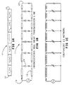
- FIG. 1A A block diagram of the pulse compressor is presented in Figure 1A.
- This pulse compressor consists of a loaded, nonlinear transmission line 11 having an input port 12 and an output port 13.
- This compressor contains n sections, the kth of which supports a soliton with a Full Width at Half Maximum (FWHM) of t k (A), where A in the amplitude of a signal travelling down the transmission line and t k+1 (A) ⁇ t k (A).
- Each section is loaded with one or more varactors.
- the inductance of the kth section is equal to the inductance per unit length of the unloaded transmission line times the length l k of the kth section.
- the capacitance per section provided by the varactors in a section is chosen to be much larger than the capacitance of that section introduced by the unloaded transmission line so that nonlinear capacitance of these varactors will introduce a significant nonlinearity in the capacitance per section.
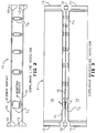
- FIG. 1B is shown an embodiment in which the transmission line is loaded with a single varactor (reverse biased Schottky diode) per section.
- the loaded transmission line consists of a first conductor 14, a second conductor 15 and a set of parallel connected reverse biased diodes 16. These reverse biased diodes provide, in each section of the transmission line, an amplitude dependent capacitance that dominates the capacitance for that section.
- An input pulse which varies with time as p(t) is applied at input port 12 and produces a signal that travels to the right along the transmission line.
- the kth varactor is centered within a section of length l k so that the capacitance per unit length of the kth section is C o + C k /l k , where C o is the intrinsic capacitance per unit length of the transmission line when it is not loaded with discrete varactors and where C k is the capacitance of the discrete varactor in the kth section.
- C o and the inductance per unit length of the transmission line are each determined by the distance d k between the two conductive lines, the width of the lines and the substrate dielectric constant within the kth section.
- the inductance per section of the kth section can be varied by varying d k and l k .
- the capacitance per section of the kth section can be varied by varying d k , C k and l k .
- transmission lines can be easily produced by forming a ground plane on one side of a substrate and forming a microstrip conductor on the other side of the substrate.
- the discrete capacitors need to make electrical contact with both the strip line and the ground plane. This can be accomplished by forming capacitors in the substrate and then forming contact vias that extend through the substrate to both the ground plane and the strip line. This necessarily requires very thin substrates.
- Imageline could also be used, but such an embodiment does not propagate signals down to dc and is not compatible with fabrication steps of most circuits. Therefore, it is preferred to use either coplanar waveguide, coplanar line or slot line embodiments. These are easily implemented because they require only single-sided metalization and are easy to integrate with active devices.
- Figure 2 presents a coplanar line version having five sections and Figure 3 presents a coplanar waveguide version having 7 sections. Each section in Figures 2 and 3 contains a single diode.
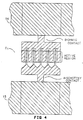
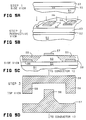
- Figure 4 shows in greater detail the structure of section 5 of the transmission line of Figure 2. The manufacture of the compressor utilizing planar technology is illustrated in Figures 5A-5D.
- epitaxial layers of doped GaAs are grown (for example, by Molecular Beam Epitaxy (MBE)) on a semi-insulating (undoped) GaAs substrate 51.
- the epitaxial layer consists of a thin, highly doped n+ layer 52 of GaAs on which is grown a second layer 53 where the doping concentration increases with distance from the top of layer 52.
- the variation in doping concentration determines the nonlinear capacitance variation with reverse bias voltage of the diodes.
- the active regions on the doped substrate where the discrete diodes will be formed are isolated from one another by proton isolation. Proton isolation makes the doped region semi-insulating by damaging the crystal structure of the doped layer.
- FIG. 5B This proton isolation step is illustrated in Figure 5B.
- a metal layer is deposited on top of layer 53 and is patterned to form a mask 54.
- the surface of layer 53 is bombarded by a beam of protons (H+) which produces a high resistivity region except where layer 53 is protected from this beam by mask 54.
- H+ protons
- Figures 5C and 5D One of these regions.
- Mask 54 is removed and contact openings 55 are formed through layer 53 to layer 52. In these contact openings are formed metal regions 56 which form the ohmic contact of the diode. On top of layer 53 is formed a metal contact 57 that forms a Schottky contact with layer 53. Metal 56 is connected to conductor 14 and metal 57 is connected to conductor 15 to couple this diode into the transmission line.
- the diodes in Figure 2 have a plurality of fingers 58 and more than two fingers 59, thereby forming a varactor that is just several diodes like that in Figure 5 connected in parallel. In all of the above steps, photolithographic techniques are used to define the active regions, ohmic regions, Schottky regions and connect metal (transmission line) regions.
- the transmission line contains 7 sections, each having a single diode contained in a "diode cell" centered on that diode.
- the transmission line contains 10 diode cells with a total length of 3.2 mm.
- the delay time indicated below is the transmission delay time through a diode cell without the diode present.
- the diodes are hyper-abrupt junction diodes (i.e., having nonuniform doping) and the parameter C k (0) of the kth cell is the zero bias junction capacitance of the Schottky diodes.
- the inductance L k of the kth section is given by the product of the delay time and the unloaded impedance.
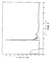
- Figure 6 shows a numerical (SPICE) simulation of the transient response of the above pulse compressor subject to a half-sine wave input pulse 61 with a full width at half maximum (FWHM) equal to 70 ps and an amplitude of 5 volts.
- FWHM full width at half maximum
- This choice of input waveform excites a single soliton which is larger in amplitude and narrower in width than the input waveshape.
- the resulting output pulse 62 has a FWHM equal to 7 ps so that there is a 10-fold compression.
- a shelf 63 of uncompressed energy which can be minimized by using more diode sections distributed over a longer length of transmission line.
- Figure 7 is a numerical simulation of a compressor having 20 diode sections.
- the overall length of the compressor can be reduced by utilizing hyperabrupt diodes with higher values of a.
- choosing the unloaded transmission line characteristic impedance to be as large as possible permits larger capacitive loading by the varactors yielding even greater compression within shorter device length.
- Every section in the transmission line need not contain just a single diode.
- each diode is contained in a "diode cell" centered on that diode.
- the transmission line contains 90 diode cells distributed in six sections.
- the delay time indicated below is the transmission delay time through a diode cell.
- the parameters for these diode cells were selected to be: k # Cells C k (fF) delay time (ps) 1 20 150 3.5886 2 10 130 3.1020 3 10 110 2.6316 4 10 90 2.1552 5 20 70 1.6747 6 20 50 1.1962
- the input pulse is triangular with a full width at half maximum (FWHM) equal to 18 ps and amplitude of 5 Volts. This choice matches reasonably well the pulse width/amplitude profile of solitons transmitted by the first section.
- the resulting output pulse has a FWHM equal to 6 ps so that there is a 3-fold compression.
- Such diodes exhibit an increased non-linearity compared to graded junction diodes and abrupt diodes.
- choosing the unloaded transmission line characteristic impedance to be as large as possible permits larger capacitive loading by the varactors yielding even greater compression within shorter device length.
Landscapes
- Physics & Mathematics (AREA)
- Nonlinear Science (AREA)
- Dc Digital Transmission (AREA)
- Reduction Or Emphasis Of Bandwidth Of Signals (AREA)
- Radar Systems Or Details Thereof (AREA)
- Communication Cables (AREA)
Applications Claiming Priority (2)
| Application Number | Priority Date | Filing Date | Title |
|---|---|---|---|
| US07/130,825 US4855696A (en) | 1987-12-09 | 1987-12-09 | Pulse compressor |
| US130825 | 1987-12-09 |
Publications (2)
| Publication Number | Publication Date |
|---|---|
| EP0320175A2 true EP0320175A2 (fr) | 1989-06-14 |
| EP0320175A3 EP0320175A3 (fr) | 1990-09-19 |
Family
ID=22446530
Family Applications (1)
| Application Number | Title | Priority Date | Filing Date |
|---|---|---|---|
| EP19880311419 Withdrawn EP0320175A3 (fr) | 1987-12-09 | 1988-12-01 | Compresseur d'impulsion |
Country Status (3)
| Country | Link |
|---|---|
| US (1) | US4855696A (fr) |
| EP (1) | EP0320175A3 (fr) |
| JP (1) | JPH01192214A (fr) |
Cited By (7)
| Publication number | Priority date | Publication date | Assignee | Title |
|---|---|---|---|---|
| GB2238199A (en) * | 1989-11-15 | 1991-05-22 | Stc Plc | Optical communications systems |
| DE10233569A1 (de) * | 2002-07-24 | 2004-02-12 | Vega Grieshaber Kg | Mikrowellen-Pulsgenerator |
| WO2003041212A3 (fr) * | 2001-11-02 | 2005-02-10 | Picosecond Pulse Labs | Echantillonneur ultrarapide comportant une ligne de choc antiparallele |
| US7084716B2 (en) | 2001-04-10 | 2006-08-01 | Picosecond Pulse Labs | Ultrafast sampler with coaxial transition |
| GB2437355A (en) * | 2002-11-13 | 2007-10-24 | Bae Systems Plc | Radio frequency or microwave signals |
| US7358834B1 (en) | 2002-08-29 | 2008-04-15 | Picosecond Pulse Labs | Transmission line voltage controlled nonlinear signal processors |
| US7612629B2 (en) | 2006-05-26 | 2009-11-03 | Picosecond Pulse Labs | Biased nonlinear transmission line comb generators |
Families Citing this family (29)
| Publication number | Priority date | Publication date | Assignee | Title |
|---|---|---|---|---|
| US5378939A (en) * | 1987-10-06 | 1995-01-03 | The Board Of Trustees Of The Leland Stanford Junior University | Gallium arsenide monolithically integrated sampling head using equivalent time sampling having a bandwidth greater than 100 Ghz |
| US5352994A (en) * | 1987-10-06 | 1994-10-04 | The Board Of Trustees Of The Leland Stanford Junior University | Gallium arsenide monolithically integrated nonlinear transmission line impedance transformer |
| US5256996A (en) * | 1987-10-06 | 1993-10-26 | The Board Of Trustees Of The Leland Stanford, Junior University | Integrated coplanar strip nonlinear transmission line |
| US5023574A (en) * | 1990-04-17 | 1991-06-11 | Hewlett-Packard Company | Nonlinear transmission lines having noncommensurate varactor cells |
| US5066928A (en) * | 1990-05-02 | 1991-11-19 | General Atomics | Soliton pulse compressor |
| US5157361A (en) * | 1991-05-10 | 1992-10-20 | Gruchalla Michael E | Nonlinear transmission line |
| DE4121569A1 (de) * | 1991-06-29 | 1993-01-14 | Standard Elektrik Lorenz Ag | Entzerrer fuer optisch uebertragene nachrichtensignale |
| US5274271A (en) * | 1991-07-12 | 1993-12-28 | Regents Of The University Of California | Ultra-short pulse generator |
| US5264800A (en) * | 1991-07-18 | 1993-11-23 | The Board Of Trustees Of The Leland Stanford, Jr. Univ. | MMIC transient capture apparatus and method |
| US5804921A (en) * | 1994-02-09 | 1998-09-08 | The Regents Of The University Of California | Soliton quenching NLTL impulse circuit with a pulse forming network at the output |
| US5495253A (en) * | 1994-11-17 | 1996-02-27 | The United States Of America As Represented By The Secretary Of The Army | Soliton rejection filter |
| US5789994A (en) * | 1997-02-07 | 1998-08-04 | Hughes Electronics Corporation | Differential nonlinear transmission line circuit |
| US6380787B1 (en) * | 1999-08-31 | 2002-04-30 | Micron Technology, Inc. | Integrated circuit and method for minimizing clock skews |
| US6559737B1 (en) * | 1999-11-24 | 2003-05-06 | The Regents Of The University Of California | Phase shifters using transmission lines periodically loaded with barium strontium titanate (BST) capacitors |
| JP2002055125A (ja) | 2000-08-08 | 2002-02-20 | Agilent Technol Inc | 標本化回路 |
| US6826208B1 (en) * | 2000-12-06 | 2004-11-30 | At&T Corp. | Nonlinear transmission line integrated circuit |
| US6538525B1 (en) * | 2000-12-19 | 2003-03-25 | Nortel Networks Limited | Voltage biased section of non-linear transmission line |
| US6737926B2 (en) * | 2001-08-30 | 2004-05-18 | Micron Technology, Inc. | Method and apparatus for providing clock signals at different locations with minimal clock skew |
| JP3848894B2 (ja) * | 2002-04-23 | 2006-11-22 | 三菱電機株式会社 | 半導体装置 |
| DE60217881D1 (de) * | 2002-11-28 | 2007-03-15 | St Microelectronics Srl | Schaltungsvorrichtung zur Herstellung eines nicht-lineares Skaliernetzwerks mit reaktiven Elementen |
| US7135917B2 (en) | 2004-06-03 | 2006-11-14 | Wisconsin Alumni Research Foundation | Left-handed nonlinear transmission line media |
| US20060125572A1 (en) * | 2004-12-09 | 2006-06-15 | Van Der Weide Daniel W | Balanced nonlinear transmission line phase shifter |
| US7456704B2 (en) * | 2005-04-29 | 2008-11-25 | California Institute Of Technology | 2D transmission line-based apparatus and method |
| US7532083B2 (en) * | 2006-03-23 | 2009-05-12 | Intel Corporation | Active nonlinear transmission line |
| JP5298415B2 (ja) * | 2006-09-05 | 2013-09-25 | 富士通株式会社 | ジッタ低減回路 |
| US8290445B2 (en) * | 2007-08-10 | 2012-10-16 | Panasonic Corporation | Electronic device, and information apparatus, communications apparatus, AV apparatus, and mobile apparatus using the same |
| US9281809B1 (en) | 2012-05-10 | 2016-03-08 | The United States Of America As Represented By The Secretary Of The Air Force | Nonlinear transmission line extraction systems |
| CN102769164A (zh) * | 2012-07-16 | 2012-11-07 | 西北核技术研究所 | 一种类同轴结构电容加载传输线 |
| WO2024130379A1 (fr) * | 2022-12-22 | 2024-06-27 | Huawei Technologies Canada Co., Ltd. | Générateurs d'impulsions électroniques et procédés associés |
Family Cites Families (7)
| Publication number | Priority date | Publication date | Assignee | Title |
|---|---|---|---|---|
| US3173026A (en) * | 1961-02-20 | 1965-03-09 | Nagumo Jin-Ichi | Active pulse transmission line |
| US3593207A (en) * | 1970-04-27 | 1971-07-13 | Us Air Force | Microwave integrated power sensitive coupler |
| US3882431A (en) * | 1973-08-10 | 1975-05-06 | Us Navy | Digital phase shifter |
| US3983416A (en) * | 1974-12-30 | 1976-09-28 | Sperry Rand Corporation | Short pulse sequential waveform generator |
| US4533840A (en) * | 1982-09-13 | 1985-08-06 | International Business Machines Corporation | Soliton sampler |
| US4701714A (en) * | 1986-03-31 | 1987-10-20 | Tektronix, Inc. | Tunable delay line |
| US4719429A (en) * | 1986-04-14 | 1988-01-12 | Ga Technologies Inc. | Transmission line microwave generator |
-
1987
- 1987-12-09 US US07/130,825 patent/US4855696A/en not_active Expired - Fee Related
-
1988
- 1988-12-01 EP EP19880311419 patent/EP0320175A3/fr not_active Withdrawn
- 1988-12-09 JP JP63311816A patent/JPH01192214A/ja active Pending
Cited By (13)
| Publication number | Priority date | Publication date | Assignee | Title |
|---|---|---|---|---|
| US5201017A (en) * | 1989-11-15 | 1993-04-06 | Stc Plc | Optical communications systems |
| GB2238199B (en) * | 1989-11-15 | 1994-06-01 | Stc Plc | Optical communications systems |
| GB2238199A (en) * | 1989-11-15 | 1991-05-22 | Stc Plc | Optical communications systems |
| US7170365B2 (en) | 2001-04-10 | 2007-01-30 | Picosecond Pulse Labs | Ultrafast sampler with non-parallel shockline |
| US7612628B2 (en) | 2001-04-10 | 2009-11-03 | Picosecond Pulse Labs | Ultrafast sampler with coaxial transition |
| US6900710B2 (en) | 2001-04-10 | 2005-05-31 | Picosecond Pulse Labs | Ultrafast sampler with non-parallel shockline |
| US7084716B2 (en) | 2001-04-10 | 2006-08-01 | Picosecond Pulse Labs | Ultrafast sampler with coaxial transition |
| WO2003041212A3 (fr) * | 2001-11-02 | 2005-02-10 | Picosecond Pulse Labs | Echantillonneur ultrarapide comportant une ligne de choc antiparallele |
| DE10233569A1 (de) * | 2002-07-24 | 2004-02-12 | Vega Grieshaber Kg | Mikrowellen-Pulsgenerator |
| US6771139B2 (en) | 2002-07-24 | 2004-08-03 | Vega Grieshaber Kg | Microwave pulse generator |
| US7358834B1 (en) | 2002-08-29 | 2008-04-15 | Picosecond Pulse Labs | Transmission line voltage controlled nonlinear signal processors |
| GB2437355A (en) * | 2002-11-13 | 2007-10-24 | Bae Systems Plc | Radio frequency or microwave signals |
| US7612629B2 (en) | 2006-05-26 | 2009-11-03 | Picosecond Pulse Labs | Biased nonlinear transmission line comb generators |
Also Published As
| Publication number | Publication date |
|---|---|
| EP0320175A3 (fr) | 1990-09-19 |
| US4855696A (en) | 1989-08-08 |
| JPH01192214A (ja) | 1989-08-02 |
Similar Documents
| Publication | Publication Date | Title |
|---|---|---|
| US4855696A (en) | Pulse compressor | |
| Rodwell et al. | Active and nonlinear wave propagation devices in ultrafast electronics and optoelectronics | |
| EP0453744B1 (fr) | Lignes de transmission non linéaires ayant des cellules de varactor inégales | |
| US5014018A (en) | Nonlinear transmission line for generation of picosecond electrical transients | |
| US6690247B2 (en) | Nonlinear transmission line waveform generator having an input voltage matched to the C/V characteristic of the transmission line | |
| US5352994A (en) | Gallium arsenide monolithically integrated nonlinear transmission line impedance transformer | |
| US5256996A (en) | Integrated coplanar strip nonlinear transmission line | |
| US5378939A (en) | Gallium arsenide monolithically integrated sampling head using equivalent time sampling having a bandwidth greater than 100 Ghz | |
| US5121067A (en) | Directional sampling bridge | |
| US4956568A (en) | Monolithic sampler | |
| US6894581B2 (en) | Monolithic nonlinear transmission lines and sampling circuits with reduced shock-wave-to-surface-wave coupling | |
| Carman et al. | V-band and W-band broadband, monolithic distributed frequency multipliers | |
| US5157361A (en) | Nonlinear transmission line | |
| US5267020A (en) | Gallium arsenide monolithically integrated sampling head using equivalent time sampling having a bandwidth greater than 100 ghz | |
| Lee | Optical control of semiconductor closing and opening switches | |
| US5155352A (en) | Optically activated sub-nanosecond hybrid pulser | |
| Proud et al. | High-frequency waveform generation using optoelectronic switching in silicon | |
| US4831340A (en) | Harmonic multiplier using resonant tunneling device | |
| US20060125572A1 (en) | Balanced nonlinear transmission line phase shifter | |
| Case et al. | Picosecond duration, large amplitude impulse generation using electrical soliton effects | |
| Baker et al. | Generation of kilovolt-subnanosecond pulses using a nonlinear transmission line | |
| Sayadian et al. | Generation of high-power broad-band microwave pulses by picosecond optoelectronic technique | |
| Kintis et al. | An MMIC pulse generator using dual nonlinear transmission lines | |
| US4114051A (en) | Triggered burst generator | |
| Lheurette et al. | Non linear transmission line quintupler loaded by heterostructure barrier varactors |
Legal Events
| Date | Code | Title | Description |
|---|---|---|---|
| PUAI | Public reference made under article 153(3) epc to a published international application that has entered the european phase |
Free format text: ORIGINAL CODE: 0009012 |
|
| AK | Designated contracting states |
Kind code of ref document: A2 Designated state(s): DE FR GB |
|
| PUAL | Search report despatched |
Free format text: ORIGINAL CODE: 0009013 |
|
| AK | Designated contracting states |
Kind code of ref document: A3 Designated state(s): DE FR GB |
|
| 17P | Request for examination filed |
Effective date: 19901109 |
|
| STAA | Information on the status of an ep patent application or granted ep patent |
Free format text: STATUS: THE APPLICATION HAS BEEN WITHDRAWN |
|
| 18W | Application withdrawn |
Withdrawal date: 19910801 |
|
| R18W | Application withdrawn (corrected) |
Effective date: 19910801 |