EP0319881A2 - Electroluminescence element - Google Patents
Electroluminescence element Download PDFInfo
- Publication number
- EP0319881A2 EP0319881A2 EP88120235A EP88120235A EP0319881A2 EP 0319881 A2 EP0319881 A2 EP 0319881A2 EP 88120235 A EP88120235 A EP 88120235A EP 88120235 A EP88120235 A EP 88120235A EP 0319881 A2 EP0319881 A2 EP 0319881A2
- Authority
- EP
- European Patent Office
- Prior art keywords
- bis
- benzene
- substrate
- organic compound
- film
- Prior art date
- Legal status (The legal status is an assumption and is not a legal conclusion. Google has not performed a legal analysis and makes no representation as to the accuracy of the status listed.)
- Withdrawn
Links
Images
Classifications
-
- C—CHEMISTRY; METALLURGY
- C09—DYES; PAINTS; POLISHES; NATURAL RESINS; ADHESIVES; COMPOSITIONS NOT OTHERWISE PROVIDED FOR; APPLICATIONS OF MATERIALS NOT OTHERWISE PROVIDED FOR
- C09K—MATERIALS FOR MISCELLANEOUS APPLICATIONS, NOT PROVIDED FOR ELSEWHERE
- C09K11/00—Luminescent, e.g. electroluminescent, chemiluminescent materials
- C09K11/06—Luminescent, e.g. electroluminescent, chemiluminescent materials containing organic luminescent materials
-
- H—ELECTRICITY
- H05—ELECTRIC TECHNIQUES NOT OTHERWISE PROVIDED FOR
- H05B—ELECTRIC HEATING; ELECTRIC LIGHT SOURCES NOT OTHERWISE PROVIDED FOR; CIRCUIT ARRANGEMENTS FOR ELECTRIC LIGHT SOURCES, IN GENERAL
- H05B33/00—Electroluminescent light sources
- H05B33/12—Light sources with substantially two-dimensional radiating surfaces
- H05B33/14—Light sources with substantially two-dimensional radiating surfaces characterised by the chemical or physical composition or the arrangement of the electroluminescent material, or by the simultaneous addition of the electroluminescent material in or onto the light source
Definitions
- the present invention relates to an electroluminescence element, and more particularly to an electroluminescence element to be used as an emitting material or luminous material for various display devices and a method of using a specified organic compound as an emitting material or luminous material of an electroluminescence element.
- An electroluminescence element (hereinafter referred to as an "EL element”) has high distinguishability because it emits light therefrom, and has impact durability because it is a complete solid element.
- an EL element using a vacuum deposited film (luminescent film) of anthracene having a film thickness of about 0.6 ⁇ m, as an emitting material, and obtained a blue visible light which is distinguishable under normal illumination at an applied voltage of 30 V (Thin Solid Films, 94 (1982), 171).
- This element is unsatisfactory in luminescent brightness and needs a high applied voltage.
- it is necessary to maintain the substrate temperature at about -50°C at the time of forming an electrode by vacuum deposition in order to prevent sublimation of the anthracene and to prevent the luminescent film from being damaged. If the substrate temperature is maintained at about room temperature, the film surface temperature rises at the time of vacuum deposition of an electrode and the luminescent film is thereby damaged and problems such as formation of short circuits between electrodes are likely to occur.
- a multi-layer film which is composed of luminous materials having electron donating and electron accepting properties, is formed by the accumulation of a monomolecular film according to the LB method and, therefore, it has problems in that the structure is complicated, the production process is also complicated and troublesome, and the element is unsuitable for practical use.
- the long chain alkyl group to be used in the monomolecular layer according to the LB method has a low heat resistant temperature of about 100°C (Kobunshi Gakkaishi, 36 1987),267). Therefore, the multi-layer film of the EL element using the LB method is damaged at the time of vacuum deposition of the opposite electrode unless special techniques such as polymerization of the monomolecule and so forth are employed. Thus the production yield of the element is seriously decreased.
- An organic EL element displaying high brightness upon application of a low voltage of less than 25 V has also been developed (Japanese Patent Application Laid-Open No.194393/1984).
- This element is a multi-layer type of electrode/positive hole injection layer/emitting layer/electrode, in which the film thickness between electrodes is necessary to be less than 0.5 ⁇ m.
- pinholes are readily formed and a serious problem arises in that productivity is low.
- An object of the present invention is to provide an EL element emitting light with high brightness upon application of a low voltage.
- Another object of the present invention is to provide an EL element which is simple in structure and can be easily produced with a high production yield, i.e., a low rejection rate.
- Still another object of the present invention is to provide a useful organic compound emitting light of high brightness as an emitting material or luminous material for an EL element.
- R1 and R2 are independently a hydrogen or an alkyl group having 1 to 4 carbon atoms
- the present invention relates to a method for using an organic compound of general formula (I) as an emitting material for an EL element.
- the present invention further relates to a thin film EL element in which a thin film of an organic compound represented by general formula (I) is sandwiched between two electrodes, at least one of which is transparent or semitransparent.
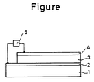
- the Figure is a schematic cross-sectional view illustrating an embodiment of the EL element of the present invention.
- Organic compounds to be used as the emitting or luminous material in the present invention are represented by the above general formula (I), which are commonly referred to as polyphenyl, polyene or stilbene-based dyes. These compounds can be synthesized by the Wittig method. Representative examples of compounds in which all of R1, R2 and R3 are hydrogen atoms, among the compounds represented by general formula (I) are shown below.
- the phenylene group i.e., a group represented by the formula: in the above formulae may be any of a p-phenylene group, a m-phenylene group and an o-phenylene group, and is preferably a p-phenylene group.
- compounds with a stilbene ring are preferred.
- Particularly preferred are trans-4,4′-diphenylstilbene and 1,4-distyryl-benzene.
- R1 and R2 of general formula (I) are alkyl groups having 1 to 4 carbon atoms (which may be hydrogen atoms), 1,4-bis(alkylstyryl)benzene derivatives represented by the general formula (I′): are preferred.
- R1 and R2 in the above general formula (I′) may be identical or different and are each an alkyl group having 1 to 4 carbon atoms, e.g., a methyl group, an ethyl group, a n-propyl group, an i-propyl group, a n-butyl group, an i-butyl group, a sec-butyl group and a tert-butyl group, or may be hydrogen atoms.
- R3 is a hydrogen atom or an alkyl group having 1 to 4 carbon atoms.
- Representative examples of the 1,4-bis(alkylstyryl)benzene derivatives represented by the general formula (I′) are 1,4-bis(2-methylstyryl)benzene, 1,4-bis(3-methylstyryl)benzene, 1,4-bis(4-methylstyryl)benzene, distyrylbenzene, 1,4-bis(2-ethylstyryl)benzene, 1,4-bis(3-ethylstyryl)benzene, 1,4-bis(2-methylstyryl)-2-methylbenzene, and 1,4-bis(2-methylstyryl)-2-ethylbenzene.
- 1,4-bis(2-methylstyryl)benzene having the formula: is particularly preferred.
- an emitting material comprising the organic compound of general formula (I) is usually used in a form of thin film.
- the thickness of the film is not critical and can be determined appropriately.
- the thickness of the film is usually 10 nm to 5 ⁇ m, preferably 0.01 to 2.0 ⁇ m.
- the thin film of the compound represented by general formula (I) can be formed by techniques such as spin coating, vacuum deposition, casting and the LB method.
- the vacuum deposition method is most preferable in that a film with good uniformity can be obtained and pinholes are less likely to be formed in the film.
- Conditions under which the thin film of a compound represented by general formula (I) is formed by the vacuum deposition method vary depending on circumstances and cannot be determined unconditionally.
- temperature for heating the boat is 100 to 400°C
- the substrate temperature is -50 to 300°C
- the pressure is 1x10 ⁇ 5 to 1x10 ⁇ 2 Pa
- the deposition rate is 0.1 to 50 nm/sec
- optimum conditions are chosen so that the film thickness is within the range of 10 nm to 5 ⁇ m.
- the organic compound can be used in various forms as the emitting material.
- the organic compound is used in such a manner that its thin film is sandwiched between two electrodes, at least one of which is transparent or semitransparent.
- an organic electroluminescence element (EL element) using a compound of general formula (I) is formed, for example, as shown in the Figure. That is, an electrode 2 in a thin film form of metal, e.g., gold, aluminum, indium, or magnesium, indium tin oxide (indium oxide doped with tin oxide; ITO), tin oxide (SnO2). zinc oxide (ZnO), copper iodide (CuI) and the like is prepared in a thickness of 10 to 1,000 nm, for example, by the sputtering method, on a supporting substrate 1 made of glass, plastics or quartz. Particularly when the thin film is intended to be transparent or semitransparent, it is formed in a thickness of 10 to 50 nm in order to ensure its transparency.
- metal e.g., gold, aluminum, indium, or magnesium
- ITO indium tin oxide doped with tin oxide
- SnO2 tin oxide
- an emitting material 3 of a compound of general formula (I) is formed in a thin film form.
- An electrode 4 is formed on the emitting material 3, so that the emitting material 3 is sandwiched between electrode 2 on supporting substrate 1 and electrode 4. It is preferred that at lease one of the electrodes 2 and 4 be transparent or semitransparent so as to allow light to pass therethrough.
- the supporting substrate 1 should also be transparent or semitransparent.
- Electrodes 2 and 4 are each connected to an electric power supply 5, e.g., an electric power supply of 10 to 70 V DC or AC.
- an electric power supply e.g., an electric power supply of 10 to 70 V DC or AC.
- the positive electrode is connected to a metal or semiconductor with a high work function, e.g., Au, Ni, Pt, SnO2 or CuI, and the negative electrode, to a metal or semiconductor with a low work function, e.g., In, Al, Mg or ITO.
- the emitting material 3 of the compound of general formula (I) Upon application of voltage from the electric source, the emitting material 3 of the compound of general formula (I) emits blue or green light.
- the supporting substrate and the electrode can be formed by usual methods using various materials.
- an organic EL element is produced using a compound of general formula (I) as an emitting material.
- a high brightness can be obtained by only application of a low voltage.
- the element is in such a simplified structure that comprises a substrate/an electrode/an emitting body (luminescent film)/an electrode and if necessary, other element, and thus can be easily produced.
- the emitting body is less subjected to damage because its material is excellent in heat resistance.
- the film thickness of the emitting body can be made relatively thick, deficiencies such as pinholes and the like can be avoided and thus productivity is increased.
- the present invention therefore, provides an EL element for various displays such as for industrial information and cars, which are inexpensive and of high quality.
- ITO Indium tin oxide
- a 25 mm x 75 mm x 1.1 mm glass substrate in a 50 nm thick film form by the sputtering method was provided on a 25 mm x 75 mm x 1.1 mm glass substrate in a 50 nm thick film form by the sputtering method to obtain a transparent substrate.
- This transparent substrate was attached to a substrate holder of a commerically available vacuum deposition system (manufactured by ULVAC Co., Ltd.), and 100 mg of 1,4-bis(2-methylstyryl)benzene was placed in an electrically-heated boat made of molybdenum. The pressure in the vacuum chamber was decreased to 5x10 ⁇ 5 Pa and the boat was heated to 160°C.
- 1,4-bis(2-methylstyryl)benzene was vapor deposited (vacuum deposited) on the transparent substrate at a deposition rate of 1.0 nm/sec to obtain a luminescent film of 0.7 ⁇ m in thickness.
- the substrate was at room temperature.
- the substrate was taken out of the vacuum chamber.
- a stainless steel mask was placed on the luminescent film of the substrate, which was then attached to the substrate holder.
- 200 mg of gold was placed, and the pressure in the vacuum chamber was decreased to 1x10 ⁇ 4 Pa. Then, the boat was heated to 1,400°C, and finally a 50 nm thick gold electrode was formed on the luminescent film to produce an organic luminescence element (EL element) in the form shown in the Figure.
- EL element organic luminescence element
- ITO was provided on a 25 mm x 75 mm x 1.1 mm glass substrate in a 50 nm thick film form by the vacuum deposition method to obtain a transparent substrate.
- This transparent substrate was attached to a substrate holder of a commercially available vacuum deposition system (manufactured by ULVAC Co., Ltd.), and 200 mg to 300 mg of trans-4,4′-diphenylstilbene prepared according to the method described in J. Org. Chem. 24, 1246 (1959) was placed in an electrically-heated boat made of molybdenum. The pressure in the vacuum chamber was decreased to 1 x 10 ⁇ 4 Pa and the boat was heated to 220°C to 240°C.
- trans-4-4′-diphenystilbene was vacuum deposited on the transparent substrate at a deposition rate of 2.0 nm/sec to obtain a luminescent film of 0.9 ⁇ m in thickness.
- the substrate was at room temperature.
- the substrate was taken out of the vacuum chamber.
- a stainless steel mask was placed on the luminescent film of the substrate, which was then attached to the substrate holder.
- 200 mg of gold was placed, and the pressure in the vacuum chamber was decreased to 2 x 10 ⁇ 4 Pa. Then, the boat was heated to 1400°C and a 50 nm thick gold electrode was formed on the luminescent film to make a counter electrode.
- EL element was produced in the same manner as in Example 2 except that 1,4-distyryl-benzene prepared according to the method described in J. Org.Chem. 24, 1246 (1959) was used as the starting material for the luminescent film, that the temperature of the boat was 240°C to 260°C, and that a luminescent film of 0.7 ⁇ m in thickness was produced.
- the melting point of 1,4-distyryl-benzene was 268°C to 269°C, and its sublimation temperature was not lower than 240°C, so the luminescent film sustained no damage at the forming of the counter electrode, and EL element was produced in a high yield.
- EL element was produced in the same manner as in Example 2 except that 1,6-diphenylhexatriene obtained by purifying a commercially available one (produced by Aldrich Chemical Company, Inc.) to be 99.5 % or higher in purity was used as the starting material for the luminescent film, that the temperature of the boat was 180°C to 190°C, and that a luminescent film of 1.3 ⁇ m in thickness was produced.
- the melting point of 1,6-diphenylhexatriene was 199°C to 203°C, and its sublimation temperature was not lower than 180°C. Accordingly, the luminescent film sustained no damage at the forming of the counter electrode, and EL element was produced in a high yield.
- ITO was provided on a 25 mm x 75 mm x 1.1 mm glass substrate in a 50 nm thick film form by the vacuum deposition method to obtain a transparent substrate.
- This transparent substrate was attached to a substrate holder of a commercially available vacuum deposition system (manufactured by ULVAC Co., Ltd.), and 200 mg of 1,4-bis(4-methylstyrtyl)benzene was placed in an electrically-heated boat made of molybdenum.
- the pressure in the vacuum chamber was decreased to 1 x 10 ⁇ 4 Pa and the boat was heated to 240°C to 246°C.
- 1,4-bis(4-methyl-styryl)benzene was vacuum deposited on the transparent substrate at a deposition rate of 0.5 to 1.0 nm/sec to obtain a luminescent film of 0.5 ⁇ m in thickness.
- the substrate was at room temperature.
- the substrate was taken out of the vacuum chamber.
- a stainless steel mask was placed on the luminescent film of the substrate, which was then attached to the substrate holder.
- 200 mg of gold was placed, and the pressure in the vacuum chamber was decreased to 2 x 10 ⁇ 4 Pa. Then, the boat was heated to 1400°C, and a 20 nm thick gold electrode was formed on the luminescent film to make a counter electrode.
- ITO was provided on a 25 mm x 75 mm x 1.1 mm glass substrate in a 50 nm thick film form by the vacuum deposition method to obtain a transparent substrate.
- This transparent substrate was attached to a substrate holder of a commercially available vacuum deposition system (manufactured by ULVAC Co., Ltd.), and 200 mg of 1,4-bis(4-ethylstyryl)benzene was placed in an electrically-heated boat made of molybdenum.
- the pressure in the vacuum chamber was decreased to 1 x 10 ⁇ 4 Pa and the boat was heated to 237°C.
- 1,4-bis(4-ethylstyryl)benzene was vacuum deposited on the transparent substrate at a deposition rate of 0.5 nm/sec to obtain a luminescent film of 0.5 ⁇ m in thickness.
- the substrate was at room temperature.
- the substrate was taken out of the vacuum chamber.
- a stainless steel mask was placed on the luminescent film of the substrate, which was then attached to the substrate holder.
- 200 mg of gold was placed, and the pressure in the vacuum chamber was decreased to 2 x 10 ⁇ 4 Pa. Then, the boat was heated to 1400°C, and a 20 nm thick gold electrode was formed on the luminescent film to make a counter electrode.
- ITO was provided on a 25 mm x 75 mm x 1.1 mm glass substrate in a 50 nm thick film form by the vacuum deposition method to obtain a transparent substrate.
- This transparent substrate was attached to a substrate holder of a commercially available vacuum deposition system (manufactured by ULVAC Co., Ltd.), and 200 mg of trans-4,4′-diphenylstilbene was placed in an electrically-heated boat made of molybdenum.
- the pressure in the vacuum chamber was decreased to 1 x 10 ⁇ 4 Pa and the boat was heated to 230°C to 245°C.
- trans-4,4′-diphenylstilbene was vacuum deposited on the transparent substrate at a deposition rate of 1.0 to 2.0 nm/sec to obtain a luminescent film of 0.5 ⁇ m in thickness.
- the temperature of the substrate was 40°C.
- the substrate was taken out of the vacuum chamber.
- a stainless steel mask was placed on the luminescent film of the substrate, which was then attached to the substrate holder.
- 200 mg of gold was placed, and the pressure in the vacuum chamber was decreased to 2 x 10 ⁇ 4 Pa. Then, the boat was heated to 1400°C, and a 20 nm thick gold electrode was formed on the luminescent film to make a counter electrode.
Abstract

Description
- The present invention relates to an electroluminescence element, and more particularly to an electroluminescence element to be used as an emitting material or luminous material for various display devices and a method of using a specified organic compound as an emitting material or luminous material of an electroluminescence element.
- An electroluminescence element (hereinafter referred to as an "EL element") has high distinguishability because it emits light therefrom, and has impact durability because it is a complete solid element. An EL element using ZnS: Mn, which is an inorganic phosphor, has been widely used. Such inorganic EL elements, however, need an applied voltage as high as about 200 V to emit light. Therefore, the driving method is complicated. In these circumstances, organic thin film EL elements using various materials are now under investigation because they permit greatly reduced applied voltages. Vincett et al. produced an EL element using a vacuum deposited film (luminescent film) of anthracene having a film thickness of about 0.6 µm, as an emitting material, and obtained a blue visible light which is distinguishable under normal illumination at an applied voltage of 30 V (Thin Solid Films, 94 (1982), 171). This element, however, is unsatisfactory in luminescent brightness and needs a high applied voltage. Moreover, in this element, it is necessary to maintain the substrate temperature at about -50°C at the time of forming an electrode by vacuum deposition in order to prevent sublimation of the anthracene and to prevent the luminescent film from being damaged. If the substrate temperature is maintained at about room temperature, the film surface temperature rises at the time of vacuum deposition of an electrode and the luminescent film is thereby damaged and problems such as formation of short circuits between electrodes are likely to occur.
- In recent years, an organic EL element emitting light with a brightness of 5 to 90 cd/m² upon application of a low voltage of about 10 V has been produced by the LB method (Langumuir-Blodgett method) (Japanese Patent Application Laid-Open Nos. 43682/1986 to 63691/1986).
- In this organic EL element, a multi-layer film, which is composed of luminous materials having electron donating and electron accepting properties, is formed by the accumulation of a monomolecular film according to the LB method and, therefore, it has problems in that the structure is complicated, the production process is also complicated and troublesome, and the element is unsuitable for practical use.
- The long chain alkyl group to be used in the monomolecular layer according to the LB method has a low heat resistant temperature of about 100°C (Kobunshi Gakkaishi, 36 1987),267). Therefore, the multi-layer film of the EL element using the LB method is damaged at the time of vacuum deposition of the opposite electrode unless special techniques such as polymerization of the monomolecule and so forth are employed. Thus the production yield of the element is seriously decreased.
- An organic EL element displaying high brightness upon application of a low voltage of less than 25 V, has also been developed (Japanese Patent Application Laid-Open No.194393/1984). This element is a multi-layer type of electrode/positive hole injection layer/emitting layer/electrode, in which the film thickness between electrodes is necessary to be less than 0.5 µm. Thus, pinholes are readily formed and a serious problem arises in that productivity is low.
- An object of the present invention is to provide an EL element emitting light with high brightness upon application of a low voltage.
- Another object of the present invention is to provide an EL element which is simple in structure and can be easily produced with a high production yield, i.e., a low rejection rate.
- Still another object of the present invention is to provide a useful organic compound emitting light of high brightness as an emitting material or luminous material for an EL element.
- The present invention relates to an EL element in which an emitting material is made of an organic compound represented by general formula (I) :


- The present invention relates to a method for using an organic compound of general formula (I) as an emitting material for an EL element.
- The present invention further relates to a thin film EL element in which a thin film of an organic compound represented by general formula (I) is sandwiched between two electrodes, at least one of which is transparent or semitransparent.
- The Figure is a schematic cross-sectional view illustrating an embodiment of the EL element of the present invention.
- Organic compounds to be used as the emitting or luminous material in the present invention are represented by the above general formula (I), which are commonly referred to as polyphenyl, polyene or stilbene-based dyes. These compounds can be synthesized by the Wittig method. Representative examples of compounds in which all of R¹, R² and R³ are hydrogen atoms, among the compounds represented by general formula (I) are shown below.

- The phenylene group, i.e., a group represented by the formula:

- When R¹ and R² of general formula (I) are alkyl groups having 1 to 4 carbon atoms (which may be hydrogen atoms), 1,4-bis(alkylstyryl)benzene derivatives represented by the general formula (I′):


- In the present invention, an emitting material comprising the organic compound of general formula (I) is usually used in a form of thin film. The thickness of the film is not critical and can be determined appropriately. The thickness of the film is usually 10 nm to 5 µm, preferably 0.01 to 2.0 µm.
- The thin film of the compound represented by general formula (I) can be formed by techniques such as spin coating, vacuum deposition, casting and the LB method. The vacuum deposition method is most preferable in that a film with good uniformity can be obtained and pinholes are less likely to be formed in the film.
- Conditions under which the thin film of a compound represented by general formula (I) is formed by the vacuum deposition method vary depending on circumstances and cannot be determined unconditionally. In a preferred embodiment of the present invention, temperature for heating the boat is 100 to 400°C, the substrate temperature is -50 to 300°C, the pressure is 1x10⁻⁵ to 1x10⁻² Pa, and the deposition rate is 0.1 to 50 nm/sec, and taking into consideration the type of compound of general formula (I), the type of the vacuum deposition system and so forth, optimum conditions are chosen so that the film thickness is within the range of 10 nm to 5 µm.
- In the EL element and the method of the present invention, the organic compound can be used in various forms as the emitting material. Preferably the organic compound is used in such a manner that its thin film is sandwiched between two electrodes, at least one of which is transparent or semitransparent.
- An organic electroluminescence element (EL element) using a compound of general formula (I) is formed, for example, as shown in the Figure. That is, an electrode 2 in a thin film form of metal, e.g., gold, aluminum, indium, or magnesium, indium tin oxide (indium oxide doped with tin oxide; ITO), tin oxide (SnO₂). zinc oxide (ZnO), copper iodide (CuI) and the like is prepared in a thickness of 10 to 1,000 nm, for example, by the sputtering method, on a supporting substrate 1 made of glass, plastics or quartz. Particularly when the thin film is intended to be transparent or semitransparent, it is formed in a thickness of 10 to 50 nm in order to ensure its transparency. Then an emitting
material 3 of a compound of general formula (I) is formed in a thin film form. An electrode 4 is formed on the emittingmaterial 3, so that the emittingmaterial 3 is sandwiched between electrode 2 on supporting substrate 1 and electrode 4. It is preferred that at lease one of the electrodes 2 and 4 be transparent or semitransparent so as to allow light to pass therethrough. When electrode 2 is transparent or semitransparent, the supporting substrate 1 should also be transparent or semitransparent. - Electrodes 2 and 4 are each connected to an electric power supply 5, e.g., an electric power supply of 10 to 70 V DC or AC. When a direct current (DC) is to be applied, the positive electrode is connected to a metal or semiconductor with a high work function, e.g., Au, Ni, Pt, SnO₂ or CuI, and the negative electrode, to a metal or semiconductor with a low work function, e.g., In, Al, Mg or ITO.
- Upon application of voltage from the electric source, the emitting
material 3 of the compound of general formula (I) emits blue or green light. - The supporting substrate and the electrode can be formed by usual methods using various materials.
- In the present invention, as described above, an organic EL element is produced using a compound of general formula (I) as an emitting material. A high brightness can be obtained by only application of a low voltage. The element is in such a simplified structure that comprises a substrate/an electrode/an emitting body (luminescent film)/an electrode and if necessary, other element, and thus can be easily produced. The emitting body is less subjected to damage because its material is excellent in heat resistance. Moreover, since the film thickness of the emitting body can be made relatively thick, deficiencies such as pinholes and the like can be avoided and thus productivity is increased. The present invention, therefore, provides an EL element for various displays such as for industrial information and cars, which are inexpensive and of high quality.
- Indium tin oxide (ITO) was provided on a 25 mm x 75 mm x 1.1 mm glass substrate in a 50 nm thick film form by the sputtering method to obtain a transparent substrate. This transparent substrate was attached to a substrate holder of a commerically available vacuum deposition system (manufactured by ULVAC Co., Ltd.), and 100 mg of 1,4-bis(2-methylstyryl)benzene was placed in an electrically-heated boat made of molybdenum. The pressure in the vacuum chamber was decreased to 5x10⁻⁵ Pa and the boat was heated to 160°C. Under these conditions, 1,4-bis(2-methylstyryl)benzene was vapor deposited (vacuum deposited) on the transparent substrate at a deposition rate of 1.0 nm/sec to obtain a luminescent film of 0.7 µm in thickness. In this vacuum deposition process, the substrate was at room temperature.
- The substrate was taken out of the vacuum chamber. A stainless steel mask was placed on the luminescent film of the substrate, which was then attached to the substrate holder. In the electrically-heated boat made of molybdenum, 200 mg of gold was placed, and the pressure in the vacuum chamber was decreased to 1x10⁻⁴ Pa. Then, the boat was heated to 1,400°C, and finally a 50 nm thick gold electrode was formed on the luminescent film to produce an organic luminescence element (EL element) in the form shown in the Figure.
- Upon application of a DC voltage of 20 V to the EL element, a current of 2.0 mA was passed and blue light was emitted. The maximum emission of the blue light was observed at the wavelength of 450 nm, and the brightness was 80 cd/m².
- ITO was provided on a 25 mm x 75 mm x 1.1 mm glass substrate in a 50 nm thick film form by the vacuum deposition method to obtain a transparent substrate. This transparent substrate was attached to a substrate holder of a commercially available vacuum deposition system (manufactured by ULVAC Co., Ltd.), and 200 mg to 300 mg of trans-4,4′-diphenylstilbene prepared according to the method described in J. Org. Chem. 24, 1246 (1959) was placed in an electrically-heated boat made of molybdenum. The pressure in the vacuum chamber was decreased to 1 x 10⁻⁴ Pa and the boat was heated to 220°C to 240°C. Under these conditions, trans-4-4′-diphenystilbene was vacuum deposited on the transparent substrate at a deposition rate of 2.0 nm/sec to obtain a luminescent film of 0.9 µm in thickness. In this vacuum deposition process, the substrate was at room temperature.
- The substrate was taken out of the vacuum chamber. A stainless steel mask was placed on the luminescent film of the substrate, which was then attached to the substrate holder. In the electrically-heated boat, 200 mg of gold was placed, and the pressure in the vacuum chamber was decreased to 2 x 10⁻⁴ Pa. Then, the boat was heated to 1400°C and a 50 nm thick gold electrode was formed on the luminescent film to make a counter electrode.
- Since the sublimation temperature (Sublimation temperature under a pressure of 2 x 10⁻⁴ Pa. The same shall apply hereinafter.) and the melting point (Melting point under atmospheric pressure. The same shall apply hereinafter.) of trans-4,4′-diphenylstilbene were 220°C or higher, the luminescent film sustained no damage at the forming of the counter electrode. Accordingly, EL element was produced in a high yield.
- Upon application of a DC voltage of 40 V to the EL element, with the gold electrode as the anode and ITO electrode as the cathode, a current of 3.1 mA was passed and pale blue light was emitted. The maximum emission of the pale blue light was observed at the wavelength of 465 nm, and the brightness was 75 cd/m².
- EL element was produced in the same manner as in Example 2 except that 1,4-distyryl-benzene prepared according to the method described in J. Org.Chem. 24, 1246 (1959) was used as the starting material for the luminescent film, that the temperature of the boat was 240°C to 260°C, and that a luminescent film of 0.7 µm in thickness was produced.
- The melting point of 1,4-distyryl-benzene was 268°C to 269°C, and its sublimation temperature was not lower than 240°C, so the luminescent film sustained no damage at the forming of the counter electrode, and EL element was produced in a high yield.
- When a DC voltage of 20 V was applied to the EL element in the same as in Example 2, a current of 10 mA was passed and purplish blue light was emitted. The maximum emission of the purplish blue was observed at the wavelength of 420 nm, and the brightness was 80 cd/m².
- EL element was produced in the same manner as in Example 2 except that 1,6-diphenylhexatriene obtained by purifying a commercially available one (produced by Aldrich Chemical Company, Inc.) to be 99.5 % or higher in purity was used as the starting material for the luminescent film, that the temperature of the boat was 180°C to 190°C, and that a luminescent film of 1.3 µm in thickness was produced.
- The melting point of 1,6-diphenylhexatriene was 199°C to 203°C, and its sublimation temperature was not lower than 180°C. Accordingly, the luminescent film sustained no damage at the forming of the counter electrode, and EL element was produced in a high yield.
- When an AC voltage of 45 V was applied to the EL element, a current of 0.29 mA was passed and greenish blue light was emitted. The maximum emission of the greenish blue light was observed at the wavelength of 447 nm, and the brightness was 1.0 cd/m².
- ITO was provided on a 25 mm x 75 mm x 1.1 mm glass substrate in a 50 nm thick film form by the vacuum deposition method to obtain a transparent substrate. This transparent substrate was attached to a substrate holder of a commercially available vacuum deposition system (manufactured by ULVAC Co., Ltd.), and 200 mg of 1,4-bis(4-methylstyrtyl)benzene was placed in an electrically-heated boat made of molybdenum. The pressure in the vacuum chamber was decreased to 1 x 10⁻⁴ Pa and the boat was heated to 240°C to 246°C. Under these conditions, 1,4-bis(4-methyl-styryl)benzene was vacuum deposited on the transparent substrate at a deposition rate of 0.5 to 1.0 nm/sec to obtain a luminescent film of 0.5 µm in thickness. In this vacuum deposition process, the substrate was at room temperature.
- The substrate was taken out of the vacuum chamber. A stainless steel mask was placed on the luminescent film of the substrate, which was then attached to the substrate holder. In the electrically-heated boat, 200 mg of gold was placed, and the pressure in the vacuum chamber was decreased to 2 x 10⁻⁴ Pa. Then, the boat was heated to 1400°C, and a 20 nm thick gold electrode was formed on the luminescent film to make a counter electrode.
- Upon application of a DC voltage of 30 V to the EL element, with the gold electrode as the anode and ITO electrode as the cathode, a current of 20 mA was passed and blue green light was emitted. The maximum emission of the blue green light was observed at the wavelength of 490 nm, the wavelength range emitted by the EL element was 440 to 560 nm, and the brightness was 60 cd/m².
- ITO was provided on a 25 mm x 75 mm x 1.1 mm glass substrate in a 50 nm thick film form by the vacuum deposition method to obtain a transparent substrate. This transparent substrate was attached to a substrate holder of a commercially available vacuum deposition system (manufactured by ULVAC Co., Ltd.), and 200 mg of 1,4-bis(4-ethylstyryl)benzene was placed in an electrically-heated boat made of molybdenum. The pressure in the vacuum chamber was decreased to 1 x 10⁻⁴ Pa and the boat was heated to 237°C. Under these conditions, 1,4-bis(4-ethylstyryl)benzene was vacuum deposited on the transparent substrate at a deposition rate of 0.5 nm/sec to obtain a luminescent film of 0.5 µ m in thickness. In this vacuum deposition process, the substrate was at room temperature.
- The substrate was taken out of the vacuum chamber. A stainless steel mask was placed on the luminescent film of the substrate, which was then attached to the substrate holder. In the electrically-heated boat, 200 mg of gold was placed, and the pressure in the vacuum chamber was decreased to 2 x 10⁻⁴ Pa. Then, the boat was heated to 1400°C, and a 20 nm thick gold electrode was formed on the luminescent film to make a counter electrode.
- Upon application of a DC voltage of 30 V to the EL element, with the gold electrode as the anode and ITO electrode as the cathode, a current of 1 mA was passed and blue green light was emitted. The maximum emission of the blue green light was observed at the wavelength of 480 nm, the wavelength range emitted by the EL element was 440 to 600 nm, and the brightness was 0.1 cd/m².
- ITO was provided on a 25 mm x 75 mm x 1.1 mm glass substrate in a 50 nm thick film form by the vacuum deposition method to obtain a transparent substrate. This transparent substrate was attached to a substrate holder of a commercially available vacuum deposition system (manufactured by ULVAC Co., Ltd.), and 200 mg of trans-4,4′-diphenylstilbene was placed in an electrically-heated boat made of molybdenum. The pressure in the vacuum chamber was decreased to 1 x 10⁻⁴ Pa and the boat was heated to 230°C to 245°C. Under these conditions, trans-4,4′-diphenylstilbene was vacuum deposited on the transparent substrate at a deposition rate of 1.0 to 2.0 nm/sec to obtain a luminescent film of 0.5 µm in thickness. In this vacuum deposition process, the temperature of the substrate was 40°C.
- The substrate was taken out of the vacuum chamber. A stainless steel mask was placed on the luminescent film of the substrate, which was then attached to the substrate holder. In the electrically-heated boat, 200 mg of gold was placed, and the pressure in the vacuum chamber was decreased to 2 x 10⁻⁴ Pa. Then, the boat was heated to 1400°C, and a 20 nm thick gold electrode was formed on the luminescent film to make a counter electrode.
- Upon application of a DC voltage of 23 V to the EL element, with the gold electrode as the anode and ITO electrode as the cathode, a current of 8 mA was passed and blue light was emitted. The maximum emission of the blue light was observed at the wavelength of 465 nm, the wavelength range emitted by the EL element was 430 to 550 nm, and the brightness was 80 cd/m².
Claims (6)


Applications Claiming Priority (4)
| Application Number | Priority Date | Filing Date | Title |
|---|---|---|---|
| JP31235687 | 1987-12-11 | ||
| JP312356/87 | 1987-12-11 | ||
| JP80257/88 | 1988-04-02 | ||
| JP63080257A JPH01254791A (en) | 1988-04-02 | 1988-04-02 | Thin-film electroluminescent element |
Publications (2)
| Publication Number | Publication Date |
|---|---|
| EP0319881A2 true EP0319881A2 (en) | 1989-06-14 |
| EP0319881A3 EP0319881A3 (en) | 1990-08-01 |
Family
ID=26421295
Family Applications (1)
| Application Number | Title | Priority Date | Filing Date |
|---|---|---|---|
| EP88120235A Withdrawn EP0319881A3 (en) | 1987-12-11 | 1988-12-03 | Electroluminescence element |
Country Status (1)
| Country | Link |
|---|---|
| EP (1) | EP0319881A3 (en) |
Cited By (11)
| Publication number | Priority date | Publication date | Assignee | Title |
|---|---|---|---|---|
| EP0387715A2 (en) * | 1989-03-15 | 1990-09-19 | Idemitsu Kosan Company Limited | Electroluminescent element |
| EP0443861A2 (en) * | 1990-02-23 | 1991-08-28 | Sumitomo Chemical Company, Limited | Organic electroluminescence device |
| US5130603A (en) * | 1989-03-20 | 1992-07-14 | Idemitsu Kosan Co., Ltd. | Organic electroluminescence device |
| EP0502202A1 (en) * | 1990-09-20 | 1992-09-09 | Idemitsu Kosan Company Limited | Organic electroluminescent element |
| WO1994015441A1 (en) * | 1992-12-18 | 1994-07-07 | Cambridge Display Technology Limited | Electroluminescent device comprising a chromophoric polymeric composition |
| EP0610514A1 (en) * | 1992-08-28 | 1994-08-17 | Idemitsu Kosan Company Limited | Charge injection assistant and organic electroluminescence device containing the same |
| WO2000041443A1 (en) | 1998-12-28 | 2000-07-13 | Idemitsu Kosan Co., Ltd. | Organic electroluminescence device |
| US6534329B2 (en) | 1991-02-27 | 2003-03-18 | The Regents Of The University Of California | Visible light emitting diodes fabricated from soluble semiconducting polymers |
| WO2003044908A2 (en) * | 2001-11-16 | 2003-05-30 | University Of Utah | Tunable blue lasers from alloys based on organic distyryl benzenesingle crystals |
| US7026061B2 (en) | 2003-03-17 | 2006-04-11 | Ritdisplay Corporation | Organic electroluminescent material and organic electroluminescent element by using the same |
| US8420874B2 (en) | 2006-10-03 | 2013-04-16 | Semiconductor Energy Laboratory Co., Ltd. | Stilbene derivative, light-emitting element, display apparatus, and electronic appliance |
Citations (5)
| Publication number | Priority date | Publication date | Assignee | Title |
|---|---|---|---|---|
| US3644211A (en) * | 1962-06-27 | 1972-02-22 | New England Nuclear Corp | Distyrylbenzene-derivative scintillator solutions |
| FR2222417A1 (en) * | 1973-03-23 | 1974-10-18 | Roth Kg Carl | Gelatinous compsn for liq. scintillation counting - contg. scintillators, hydrocarbon solvent and non-ionic emulsifier |
| JPS5474692A (en) * | 1977-11-28 | 1979-06-14 | Nippon Telegr & Teleph Corp <Ntt> | Photo conversion system of integration current by electrolytic chemiluminescence |
| SU691477A1 (en) * | 1977-07-25 | 1979-10-15 | Предприятие П/Я Р-6496 | Luminescent penetrant |
| JPS6144986A (en) * | 1984-08-10 | 1986-03-04 | Canon Inc | El element |
-
1988
- 1988-12-03 EP EP88120235A patent/EP0319881A3/en not_active Withdrawn
Patent Citations (5)
| Publication number | Priority date | Publication date | Assignee | Title |
|---|---|---|---|---|
| US3644211A (en) * | 1962-06-27 | 1972-02-22 | New England Nuclear Corp | Distyrylbenzene-derivative scintillator solutions |
| FR2222417A1 (en) * | 1973-03-23 | 1974-10-18 | Roth Kg Carl | Gelatinous compsn for liq. scintillation counting - contg. scintillators, hydrocarbon solvent and non-ionic emulsifier |
| SU691477A1 (en) * | 1977-07-25 | 1979-10-15 | Предприятие П/Я Р-6496 | Luminescent penetrant |
| JPS5474692A (en) * | 1977-11-28 | 1979-06-14 | Nippon Telegr & Teleph Corp <Ntt> | Photo conversion system of integration current by electrolytic chemiluminescence |
| JPS6144986A (en) * | 1984-08-10 | 1986-03-04 | Canon Inc | El element |
Non-Patent Citations (3)
| Title |
|---|
| DERWENT FILE SUPPLIER WPIL, AN 79-55282b (30), Derwent Publications Ltd, London, GB; & JP-A-54 074 692 (NIPPON TELEG. & TELEPH.) * |
| DERWENT FILE SUPPLIER WPIL, AN 80-40957C (23), Derwent Publications Ltd, London, GB; & SU-A-69 1477 (MALKES et al.) * |
| DERWENT FILE SUPPLIER WPIL, AN 86-220726 (34), Derwent Publications Ltd, London, GB; & JP-A-61 044 986 (CANON) * |
Cited By (26)
| Publication number | Priority date | Publication date | Assignee | Title |
|---|---|---|---|---|
| EP0387715A3 (en) * | 1989-03-15 | 1991-07-17 | Idemitsu Kosan Company Limited | Electroluminescent element |
| US5126214A (en) * | 1989-03-15 | 1992-06-30 | Idemitsu Kosan Co., Ltd. | Electroluminescent element |
| EP0387715A2 (en) * | 1989-03-15 | 1990-09-19 | Idemitsu Kosan Company Limited | Electroluminescent element |
| EP0616020A1 (en) | 1989-03-20 | 1994-09-21 | Idemitsu Kosan Company Limited | Aromatic dimethylidyne compounds and process for preparation thereof |
| US5130603A (en) * | 1989-03-20 | 1992-07-14 | Idemitsu Kosan Co., Ltd. | Organic electroluminescence device |
| US6093864A (en) * | 1989-03-20 | 2000-07-25 | Idemitsu Kosan Co., Ltd. | Aromatic dimethylidyne compounds |
| EP0443861A2 (en) * | 1990-02-23 | 1991-08-28 | Sumitomo Chemical Company, Limited | Organic electroluminescence device |
| EP0443861A3 (en) * | 1990-02-23 | 1992-03-11 | Sumitomo Chemical Company, Limited | Organic electroluminescence device |
| US5317169A (en) * | 1990-02-23 | 1994-05-31 | Sumitomo Chemical Company, Limited | Organic electroluminescence device |
| US5726457A (en) * | 1990-02-23 | 1998-03-10 | Sumitomo Chemical Company, Limited | Organic electroluminescence device |
| EP0502202A4 (en) * | 1990-09-20 | 1995-02-22 | Idemitsu Kosan Co | Organic electroluminescent element |
| EP0502202A1 (en) * | 1990-09-20 | 1992-09-09 | Idemitsu Kosan Company Limited | Organic electroluminescent element |
| US6878974B2 (en) | 1991-02-27 | 2005-04-12 | The Regents Of The University Of California | Visible light emitting diodes fabricated from soluble semiconducting polymers |
| US6534329B2 (en) | 1991-02-27 | 2003-03-18 | The Regents Of The University Of California | Visible light emitting diodes fabricated from soluble semiconducting polymers |
| EP1056140A3 (en) * | 1992-08-28 | 2002-01-02 | Idemitsu Kosan Company Limited | Charge injection auxiliary material |
| EP0610514A1 (en) * | 1992-08-28 | 1994-08-17 | Idemitsu Kosan Company Limited | Charge injection assistant and organic electroluminescence device containing the same |
| EP0610514A4 (en) * | 1992-08-28 | 1994-10-12 | Idemitsu Kosan Co | Charge injection assistant and organic electroluminescence device containing the same. |
| EP1056140A2 (en) * | 1992-08-28 | 2000-11-29 | Idemitsu Kosan Company Limited | Charge injection auxiliary material |
| WO1994015441A1 (en) * | 1992-12-18 | 1994-07-07 | Cambridge Display Technology Limited | Electroluminescent device comprising a chromophoric polymeric composition |
| US5653914A (en) * | 1992-12-18 | 1997-08-05 | Cambridge Display Technology Limited | Electroluminescent device comprising a chromophoric polymeric composition |
| WO2000041443A1 (en) | 1998-12-28 | 2000-07-13 | Idemitsu Kosan Co., Ltd. | Organic electroluminescence device |
| EP2270117A2 (en) | 1998-12-28 | 2011-01-05 | Idemitsu Kosan Co., Ltd. | Organic electroluminescence device |
| WO2003044908A2 (en) * | 2001-11-16 | 2003-05-30 | University Of Utah | Tunable blue lasers from alloys based on organic distyryl benzenesingle crystals |
| WO2003044908A3 (en) * | 2001-11-16 | 2004-07-01 | Univ Utah | Tunable blue lasers from alloys based on organic distyryl benzenesingle crystals |
| US7026061B2 (en) | 2003-03-17 | 2006-04-11 | Ritdisplay Corporation | Organic electroluminescent material and organic electroluminescent element by using the same |
| US8420874B2 (en) | 2006-10-03 | 2013-04-16 | Semiconductor Energy Laboratory Co., Ltd. | Stilbene derivative, light-emitting element, display apparatus, and electronic appliance |
Also Published As
| Publication number | Publication date |
|---|---|
| EP0319881A3 (en) | 1990-08-01 |
Similar Documents
| Publication | Publication Date | Title |
|---|---|---|
| US5121029A (en) | Electroluminescence device having an organic electroluminescent element | |
| JP4584272B2 (en) | Blue light emitting compound for organic electroluminescent device and organic electroluminescent device using the same | |
| US5487953A (en) | Organic electroluminescent device | |
| KR100258776B1 (en) | Organic electroluminescent element | |
| EP0373582B1 (en) | Electroluminescence device | |
| EP0319881A2 (en) | Electroluminescence element | |
| JPH0613181A (en) | Emission method of organic thin film light emitting element | |
| JPH01245087A (en) | Organic electroluminescence element | |
| JPH04304466A (en) | Organic thin-film light emitting element | |
| JP4154215B2 (en) | Method for manufacturing organic electroluminescence display element | |
| KR20020075894A (en) | Organic electroluminescence device | |
| KR100826439B1 (en) | Organic electroluminescent devices | |
| JP3546697B2 (en) | Organic EL device | |
| JPH01254791A (en) | Thin-film electroluminescent element | |
| JPH0693256A (en) | Organic thin-film luminescent element | |
| JP3614365B2 (en) | Thin film EL device | |
| JP2003321402A (en) | Adamantane derivative, method for producing the same and organic electroluminescent element using adamantane derivative | |
| JP2731971B2 (en) | Electroluminescence element | |
| JP2000231988A (en) | Organic electroluminescent element | |
| JPH11204265A (en) | Organic thin film luminescent element | |
| JP3755692B2 (en) | Organic thin film light emitting device | |
| JPH10255980A (en) | Organic thin film luminescent element | |
| JP2000252064A (en) | Organic electroluminescent element | |
| KR0146019B1 (en) | Organic material for electroluminescent device and electroluminescent device | |
| JP2000252066A (en) | Organic electroluminescent element |
Legal Events
| Date | Code | Title | Description |
|---|---|---|---|
| PUAI | Public reference made under article 153(3) epc to a published international application that has entered the european phase |
Free format text: ORIGINAL CODE: 0009012 |
|
| AK | Designated contracting states |
Kind code of ref document: A2 Designated state(s): BE CH DE FR GB IT LI NL SE |
|
| PUAL | Search report despatched |
Free format text: ORIGINAL CODE: 0009013 |
|
| AK | Designated contracting states |
Kind code of ref document: A3 Designated state(s): BE CH DE FR GB IT LI NL SE |
|
| 17P | Request for examination filed |
Effective date: 19901215 |
|
| 17Q | First examination report despatched |
Effective date: 19911028 |
|
| STAA | Information on the status of an ep patent application or granted ep patent |
Free format text: STATUS: THE APPLICATION IS DEEMED TO BE WITHDRAWN |
|
| 18D | Application deemed to be withdrawn |
Effective date: 19930615 |