EP0319021B1 - Apparatus for laser chemical vapour deposition - Google Patents
Apparatus for laser chemical vapour deposition Download PDFInfo
- Publication number
- EP0319021B1 EP0319021B1 EP19880120152 EP88120152A EP0319021B1 EP 0319021 B1 EP0319021 B1 EP 0319021B1 EP 19880120152 EP19880120152 EP 19880120152 EP 88120152 A EP88120152 A EP 88120152A EP 0319021 B1 EP0319021 B1 EP 0319021B1
- Authority
- EP
- European Patent Office
- Prior art keywords
- laser beam
- deposition substrate
- laser
- angle
- deposition
- Prior art date
- Legal status (The legal status is an assumption and is not a legal conclusion. Google has not performed a legal analysis and makes no representation as to the accuracy of the status listed.)
- Expired - Lifetime
Links
Images


Classifications
-
- C—CHEMISTRY; METALLURGY
- C23—COATING METALLIC MATERIAL; COATING MATERIAL WITH METALLIC MATERIAL; CHEMICAL SURFACE TREATMENT; DIFFUSION TREATMENT OF METALLIC MATERIAL; COATING BY VACUUM EVAPORATION, BY SPUTTERING, BY ION IMPLANTATION OR BY CHEMICAL VAPOUR DEPOSITION, IN GENERAL; INHIBITING CORROSION OF METALLIC MATERIAL OR INCRUSTATION IN GENERAL
- C23C—COATING METALLIC MATERIAL; COATING MATERIAL WITH METALLIC MATERIAL; SURFACE TREATMENT OF METALLIC MATERIAL BY DIFFUSION INTO THE SURFACE, BY CHEMICAL CONVERSION OR SUBSTITUTION; COATING BY VACUUM EVAPORATION, BY SPUTTERING, BY ION IMPLANTATION OR BY CHEMICAL VAPOUR DEPOSITION, IN GENERAL
- C23C16/00—Chemical coating by decomposition of gaseous compounds, without leaving reaction products of surface material in the coating, i.e. chemical vapour deposition [CVD] processes
- C23C16/44—Chemical coating by decomposition of gaseous compounds, without leaving reaction products of surface material in the coating, i.e. chemical vapour deposition [CVD] processes characterised by the method of coating
- C23C16/48—Chemical coating by decomposition of gaseous compounds, without leaving reaction products of surface material in the coating, i.e. chemical vapour deposition [CVD] processes characterised by the method of coating by irradiation, e.g. photolysis, radiolysis, particle radiation
- C23C16/483—Chemical coating by decomposition of gaseous compounds, without leaving reaction products of surface material in the coating, i.e. chemical vapour deposition [CVD] processes characterised by the method of coating by irradiation, e.g. photolysis, radiolysis, particle radiation using coherent light, UV to IR, e.g. lasers
-
- C—CHEMISTRY; METALLURGY
- C23—COATING METALLIC MATERIAL; COATING MATERIAL WITH METALLIC MATERIAL; CHEMICAL SURFACE TREATMENT; DIFFUSION TREATMENT OF METALLIC MATERIAL; COATING BY VACUUM EVAPORATION, BY SPUTTERING, BY ION IMPLANTATION OR BY CHEMICAL VAPOUR DEPOSITION, IN GENERAL; INHIBITING CORROSION OF METALLIC MATERIAL OR INCRUSTATION IN GENERAL
- C23C—COATING METALLIC MATERIAL; COATING MATERIAL WITH METALLIC MATERIAL; SURFACE TREATMENT OF METALLIC MATERIAL BY DIFFUSION INTO THE SURFACE, BY CHEMICAL CONVERSION OR SUBSTITUTION; COATING BY VACUUM EVAPORATION, BY SPUTTERING, BY ION IMPLANTATION OR BY CHEMICAL VAPOUR DEPOSITION, IN GENERAL
- C23C16/00—Chemical coating by decomposition of gaseous compounds, without leaving reaction products of surface material in the coating, i.e. chemical vapour deposition [CVD] processes
- C23C16/44—Chemical coating by decomposition of gaseous compounds, without leaving reaction products of surface material in the coating, i.e. chemical vapour deposition [CVD] processes characterised by the method of coating
- C23C16/48—Chemical coating by decomposition of gaseous compounds, without leaving reaction products of surface material in the coating, i.e. chemical vapour deposition [CVD] processes characterised by the method of coating by irradiation, e.g. photolysis, radiolysis, particle radiation
- C23C16/488—Protection of windows for introduction of radiation into the coating chamber
Description
- The present invention relates generally to the manufacture of a semiconductor device, and, more specifically, to an apparatus for performing a method for forming a deposition film using a laser CVD technique by irradiating a reaction gas with a laser beam, generating a reaction product through decomposition and reaction of reaction gas and forming the reaction product on a substrate.
- It is generally known to form a thin film of polysilicon and oxide on a semiconductor substrate by chemical vapour deposition (CVD), in which a reaction gas is introduced into a processing chamber containing a semiconductor substrate, a reaction product is formed by reaction of the reaction gas, and the reaction product is deposited on the semi conductor substrate.
- One such CVD method is the laser CVD method, wherein the reaction gas is irradiated with a laser beam, a reaction product is formed by decomposition and reaction of the reaction gas, and the reaction product is deposited on a substrate. This method has an advantage that damage to the semiconductor substrate surface is minimised by realising growth of a deposition product at a temperature lower than that of a thermal CVD method for thermally decomposing the reaction gas. Also, the laser CVD method assures that plasma energy for the energy of laser used will be lower than that in the non-CVD methods. With such advantages, the laser CVD technique has great potential for future use in wider applications for semiconductor devices.
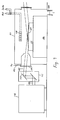
- Fig. 7 of the accompanying drawings is a schematic cross-sectional view of a known laser CVD apparatus in which a
laser beam 100 passes through areaction chamber 101 through a laserbeam inlet port 102. An O-ring 103 andsynthetic quartz window 104 are disposed at theinlet port 102. Agas inlet port 105 is provided for introducing a purge gas, while asupport base 106 supports adeposition substrate 107 on aheater 111. A reaction gas is introduced through reactiongas inlet port 108, and exhausted throughexhaust port 109. Alens system 110 is also provided. - The laser CVD apparatus of Fig. 7 is used for depositing SiO₂. First, the gas in the
reaction chamber 101 is exhausted from theexhaust port 109 and the interior ofreaction chamber 101 is kept at a constant pressure. Thereafter, the reaction gas, which may include N₂O and Si₂H₆, is introduced into thereaction chamber 101 from the reactiongas inlet port 108. Simultaneously, N₂ is introduced through thegas inlet port 105 for purging in order to prevent the reaction gas from contacting the laserbeam inlet port 102. When the inside of thereaction chamber 101 is exposed to thelaser beam 100 which passes through thesynthetic quartz window 104 fixed by the O-ring 103, only the reaction gas irradiated by the laser beam is decomposed and reacts, generating a radical beam (indicated by X marks) that appears purple. Thereby, SiO₂ is produced and deposited on thedeposition substrate 107. - Figs. 6(a)-6(c) are schematic diagrams illustrating a method of forming a deposition film utilising the aforementioned known laser CVD technique. Fig. 7 corresponds to Fig. 6(a).
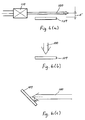
- These Figures illustrate a
laser beam 100, adeposition substrate 107, and alens system 110 for converging thelaser beam 100. Fig. 6(a) is a profile for horizontal irradiation where thelaser beam 100 is emitted horizontally relative to thedeposition substrate 107. Fig. 6(b) is a profile for vertical irradiation where thelaser beam 100 is emitted vertically relative to thedeposition substrate 107, and Fig. 6(c) is a profile for inclined irradiation where thelaser beam 100 is emitted at an inclination angle of 45° relative to thedeposition substrate 107. - All three of the above methods have been used to form a deposition film. However, these methods have the following problems:
By the method employing horizontal irradiation, a deposition film can be deposited on a large area but it is difficult to set a clearance d′ between the laser beam anddeposition substrate 107. If the clearance becomes too large, reaction products combine to create a reaction product powder having a large particle size. When deposited on the substrate, this powder deteriorates film quality. Moreover, since the reaction product is deposited from above, the deposition substrate surface is not irradiated with the laser beam and surface reaction is not easily generated at the surface of the substrate. Also, step coverage is poor in cases where the surface of thedeposition substrate 107 includes step and shoulder portions which project from or are recessed into the substrate. - In this method, the energy per unit area must be raised by converging the laser beam with a
special lens system 110 called a cylindrical lens in order to raise the deposition rate, and thus the apparatus employed in the method is large and complicated. Moreover, the energy of the laser beam is partly absorbed by thelens system 110 when the laser beam passes therethrough. Therefore, the energy efficiency of the laser beam is deteriorated. - For the method employing vertical irradiation, the irradiation area is narrow because it corresponds to the cross-sectional size of the laser beam. Moreover, the beam size must be enlarged by applying the
laser beam 100 to a lens system (not illustrated). However, energy efficiency of the laser beam is deteriorated because the laser beam energy is partly absorbed by the lens system when the laser beam passes through the lens system. - In the method employing irradiation inclined at a 45° angle, a problem similar to that associated with vertical irradiation is experienced.
- EP-A-0 229 633 discloses a laser CVD apparatus for forming a deposition film on a deposition substrate, comprising:
a laser source, and
a reaction chamber having a laser inlet port through which a laser beam from the laser source can enter the reaction chamber for irradiating a reaction gas in the reaction chamber with the laser beam, thereby to produce a reaction product by decomposition and reaction of said reaction gas, and deposit said reaction product on a surface of the deposition substrate arranged in the reaction chamber. - In the apparatus of EP-A-0 229 633 the beam passes through the chamber substantially parallel, and contiguous, to the substrate. This, it is stated, is preferably achieved by lenses between the laser source and the laser inlet port.
- It is stated that as the beam moves through the chamber, it loses energy.
- For compensating for this stated loss of energy as the beam moves through the chamber it is proposed that the substrate be tilted slightly, to decrease the distance between the beam and the substrate as the beam moves through the substrate. It is also proposed that, for the same purpose, the beam may be tapered in the direction along the substrate.
- It is suggested that (additional) lenses may be included in the laser inlet port (window) for producing the desired configuration of the beam.
- The present invention solves the problems associated with known methods as explained above. It is therefore an object of the present invention to provide apparatus for performing a laser CVD technique which assures a large irradiation area without lowering laser beam energy.
- Another object of the invention is to provide a laser CVD apparatus having a capability for easy adjustment of the irradiation angle of the laser beam relative to the deposition substrate.
- According to the present invention there is provided a laser CVD apparatus for forming a deposition film on a deposition substrate, comprising:
a laser source, and
a reaction chamber having a laser inlet port through which a laser beam from the laser source can enter the reaction chamber for irradiating a reaction gas in the reaction chamber with the laser beam, thereby to produce a reaction product by decomposition and reaction of said reaction gas, and deposit said reaction product on a surface of the deposition substrate arranged in the reaction chamber,
characterised in that
the apparatus further comprises a beam angle setting mechanism, between the laser source (114) and the laser inlet port, operable to project the laser beam onto the surface of the deposition substrate arranged in the reaction chamber and to set the angle of incidence of the laser beam, in its direction of propagation, for contacting and irradiating the surface of the deposition substrate, at a relatively low angle selected such that the deposition substrate is all included within the beam range of the laser beam in its direction of propagation,
and in that the apparatus lacks any lens system between the laser source and the surface of the deposition substrate arranged in the reaction chamber. - The present invention is capable of expanding the irradiation area without using a lens system by irradiating the deposition substrate surface with the laser beam at a relatively low angle. As explained above, the present invention does not require the use of a lens system to expand the beam diameter of the laser beam. Therefore, the laser beam energy is not lowered by the lens system. Moreover, adjustment of clearance between the laser beam and the deposition substrate is no longer necessary, unlike in horizontal irradiation.
- In addition, even if the deposition substrate surface has projecting and/or recessed portions, since the laser beam repeats its reflection in these projecting and recessed portions by irradiating the uneven surfaces with the laser beam at a small angle, the parts behind the projecting and recessed portions and the stepped portion are also irradiated with the laser beam, and thus, step coverage is improved.
- Embodiments of the invention will now be described in more detail with reference to the accompanying drawings, in which:
- Fig. 1 is a sectional view of an apparatus embodying the present invention;
- Figs. 2(a) to 2(c) are schematic diagrams illustrating a method of forming a deposition film implemented in the apparatus according to the present invention;
- Fig. 3 is a schematic diagram illustrating the effect on a stepped surface of a low-angled laser beam according to the present invention;
- Fig. 4 is a graph illustrating comparative deposition rates obtained with the apparatus according to the present invention and with prior apparatuses;
- Fig. 5 is a schematic diagram illustrating a method of setting the irradiation angle of the laser beam which can be employed with the apparatus according to the present invention;
- Fig. 6(a) to 6(c) are schematic sectional views illustrating a known laser beam irradiation method; and
- Fig. 7 is a schematic sectional view of a known laser CVD apparatus.
- A preferred embodiment of an apparatus embodying the present invention is shown in Fig. 1.
- Fig. 1 illustrates a
laser beam 100 which enters areaction chamber 101 through alaser inlet port 102 and asynthetic quartz window 104. Agas inlet port 105 introduces gas for purging. Astage 106 movable horizontally in the X and Y directions supports aheater 111, and adeposition substrate 107 is placed on theheater 111. A reactiongas inlet port 108 introduces reaction gas into thereaction chamber 101. A beamangle setting mechanism 112 includes amirror body 113 and an ArFexcimer laser source 114. Although there are many different types of lasers, the "excimer" laser is preferred. An excimer laser is a laser containing a noble gas, such as argon, which is based on a transition between an excited state in which a metastable bond exists between two gas atoms and a rapidly dissociating ground state. When being separated into two atoms, the excimer laser produces ultraviolet radiation corresponding to the difference between energy levels, and thus, the excimer laser is produced by ultraviolet radiation. As an example, SiO₂, which is obtained from the coupling of N₂O and Si₂H₆, is stable so that it does not change to another state. In contrast, ArF is obtained from the coupling of Ar and F and is very unstable so that it easily divides into the original atoms, Ar and F. In the process of separating into Ar and F, an ultraviolet radiation excimer laser is produced. - The laser CVD apparatus of Fig. 1 is used for depositing SiO₂. First, the gas in the
reaction chamber 101 is exhausted from theexhaust port 109 to keep the pressure within thereaction chamber 101, for example, at about 4 Torr. Next, the reaction gas, which includes N₂O and Si₂H₆, is introduced into thereaction chamber 101 in the amount of about 200 SCCM and 0.2 SCCM, respectively, from the reactiongas inlet port 108. The reaction gas may also be a mixture of N₂O + Si₃H₈, O₂ + Si₃H₆, or O₂ + Si₃H₈. For depositing a SiN layer, NH₃ + Si₂H₆ or NH₃ + Si₃H₈ may be used. For an Si layer, Si₈H₆ and Si₃H₈ may be used. While an ArF gas is used for the excimer laser, it is possible to use KrF gas in the case of depositing an Si layer with Si₃H₆. - The reaction
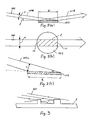
gas inlet port 108 is preferably provided in proximity to thedeposition substrate 107 in order to prevent the generation of reaction product in unwanted areas of thereaction chamber 101. Next, the purge gas, N₂ for example, in amount of 10 litres/minute is supplied from the purginggas inlet port 105 in order to prevent the reaction gas from entering thelaser inlet port 102 and thereby causing thesynthetic quartz window 104 to become cloudy. Thereafter, thedeposition substrate 107 disposed on theheater 111 is heated up to a temperature of about 300°C. Next, thelaser beam 100 is guided to the reaction chamber through thesynthetic quartz window 104. The laser beam is a pulsed ArF excimer laser, for example, with an output of 12 W, a frequency of 50 Hz, pulse energy of 240 mJ and a wavelength of 198 nm. The beam has a width of about 1 cm and a height of about 2 cm when emitted from thelaser source 114. As explained above, when the inside of thereaction chamber 101 is exposed to thelaser beam 100, the reaction gas generates a radical beam of purple appearance through decomposition and reaction of only the gas exposed to the laser beam. The SiO₂ thus generated is gradually deposited on thedeposition substrate 107. - Figs. 2(a) and 2(b) are schematic diagrams illustrating the laser beam which is irradiated on the deposition substrate according to a preferred embodiment of the present invention. Fig. 2(a) is a sectional view and Fig. 2(b) is a top plan view. Fig. 3 is a schematic sectional view for explaining the improvement in step coverage in a preferred embodiment of the present invention. Fig. 4 is a graph showing the effect on the deposition rate obtained with an apparatus according to the present invention in comparison with that obtained with a known apparatus.
- In these Figures, a
deposition substrate 107 has aregion 2 on which a deposition film is formed. Theregion 2 has a length defined between the opposite ends 10 and 11 of thedeposition substrate 107. The width of theregion 2 is defined by thewidth 4 of thelaser beam 100. - As indicated in Figs. 2(a) and 2(b), a
deposition substrate 107, for example, a flat plate having a diameter of about 10 cm, is placed in an appropriate position in an atmosphere including the reaction gas (Si₂H₆ and N₂O). Thereafter, thedeposition substrate 107 is irradiated With thelaser beam 100, e.g. the ArF excimer laser beam, such that the laser beam is projected on the surface ofdeposition substrate 107. In this case, the angle of incidence of thelaser beam 100 in its direction of propagation which contacts tie deposition substrate at least completely includes the length oftie region 2 defined between the opposite ends 10 arid 11 of thedeposition substrate 107. - If the
laser beam 100 to be irradiated has awidth 4 of 4 cm and aheight 5 of 1 cm, the angle ofincidence 3, which is also the angle of irradiation, is about 6°. Moreover, in case theheight 5 of thebeam 100 is 1 cm andwidth 4 is 4 cm, the irradiation angle of about 4° to 10° is necessary to irradiate completely theregion 2 having a size of from about 1.6 to 15.2 cm (3 to 6 inches). - In the method of forming a deposition film using the laser CVD technique described heretofore, implemented in the apparatus embodying the invention, a deposition film is formed in a wider area on the substrate surface, even without using a lens system for expanding the beam diameter of the laser beam. This is accomplished by setting the angle of incidence to such a low angle that the laser beam strikes the entire length of the deposition substrate in the irradiation direction of the laser beam. Moreover, since a lens system is not employed, energy loss of the laser beam is reduced, and thus, energy efficiency of the laser beam is enhanced.
- Fig. 5 is a schematic diagram illustrating a method for setting the irradiation angle or angle of incidence of the
laser beam 100 for a deposition substrate and laser beam of a particular size, which method can be implemented in the apparatus embodying the present invention. - This figure illustrates a
fluorescent plate 115, a beamangle adjusting mechanism 112, arid amirror body 113. The distance "d" is the distance between the ArFexcimer laser source 114 and thefluorescent plate 115. - First, prior to forming the thin film on the deposition substrate with the laser CVD technique, a substance which generates fluorescence when irradiated by the
laser beam 100, such as afluorescent plate 115, is set on theheater 111 on which the deposition substrate is to be set within thereaction chamber 101. Next, when the ArFexcimer laser source 114 is turned ON, thelaser beam 100 irradiates thefluorescent plate 115 after passing from the ArFexcimer laser source 114, through the beamangle adjusting mechanism 112 andsynthetic quartz window 104. Next, the beam angle is adjusted with a beamangle adjusting mechanism 112 so that the irradiation range "b" for thefluorescent plate 115 of the laser beam becomes at least as long as a diameter (lengthwise) of the deposition substrate to be deposited later. The range b is the distance that the laser beam travels over thefluorescent plate 115, and eventually, thedeposition substrate 107. The beamangle adjusting mechanism 112 has amirror body 113 and the irradiation angle of the laser beam relative to the deposition substrate can be set by adjusting the angle and/or height of thelaser beam 100 emanating from themirror body 113. Adjustment of the mirror body may be done with a driving apparatus (not illustrated) or manually. - Adjustment of the beam diameter will now be explained. As described previously, the laser beam generated from the ArF
excimer laser source 114 in one embodiment has a width of 2 cm and a height of 1 cm. Since this laser beam has an intrinsic beam divergence, the beam diameter becomes larger until it reaches thefluorescent plate 115. Therefore, the beam diameter can be adjusted to a certain degree by adjusting the distance "d" between the ArFexcimer laser source 114 and thefluorescent plate 115. - After setting the irradiation angle of the laser beam according to the steps described above, the
fluorescent plate 115 is taken out from thereaction chamber 101 and a deposition substrate is then set on theheater 111 in place of thefluorescent plate 115. The deposition substrate can now easily be irradiated with the laser beam at the desired angle. - However, as shown in Fig. 2(b), a thin film can be formed on only a part of the
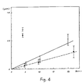
deposition substrate 107 so long as the positions of the deposition substrate and the laser beam are fixed. Accordingly, thestage 106 supporting thedeposition substrate 107 is moved in a direction perpendicular to the direction of beam irradiation at a rate, for example, of 2 cm/second, or thelaser beam 100 is scanned to the right and left at a rate, e.g. of 2 cm/second in order to form a thin film on the entire part of the deposition substrate 1. However, when the laser beam is scanned, the driving mechanism of the beamangle setting apparatus 112 is complicated and thesynthetic quartz window 104 of thereaction chamber 101 must also be formed larger in size. Therefore, it is preferable to employ the method of moving thestage 106 instead of moving the beam. - Fig. 4 is a graph indicating the relationship between the irradiation time and deposition film thickness when a laser beam with an output of 12 W, a frequency of 50 Hz and a pulse energy of 240 mJ is used. In this Figure, a solid line indicates the relationship between the irradiation time and the deposition film thickness obtained by using a small angle of irradiation for the laser beam according to the present invention, while a broken line indicates the relationship between tie irradiation time and the deposition film thickness obtained by using a parallel irradiation laser beam. As will be apparent from the Figure, the method implemented in the apparatus embodying the present invention assures a faster deposition rate due to the generation of a reaction of the reaction gas in a region closer to the deposition substrate. The known apparatus, in contrast, produce reaction product in a region spaced from the deposition substrate and deposits the same at regions other than the deposition substrate.
- Moreover, a shown in Fig. 3, when the surface of the deposition substrate has projecting and recessed portions (depth of about 1 µm) and is irradiated at a low angle With the laser beam, the laser beam is reflected into and irradiates the projecting and recessed portions of surface and thereby improves step coverage in comparison with the known methods corresponding to Fig. 6(a). Accordingly, the reaction product produced in the vicinity of the deposition substrate is also deposited on the deposition substrate. Moreover, the recessed part of substrate surface is also irradiated with the laser beam and reaction product generated by irradiation is further deposited on the substrate.
- The irradiation angle of the laser beam as described throughout the present disclosure refers to the angle at which the
laser beam 100 is emitted into the reaction chamber. The irradiation angle is equal to the angle of incidence, which refers to the angle at which the laser beam strikes either thedeposition substrate 107 or thefluorescent plate 115. Another aspect of the present invention is to determine the maximum acceptable angle of incidence (ϑ₀) and to adjust the angle of incidence according to that determination. As previously stated, the irradiation angle is preferably adjusted in such a way that the laser beam is at a low angle so that thesubstrate 107 is all included within a range of the laser beam. Thus, as shown in Fig. 2(a), the range of the laser beam coincides with the length "a", which is the length of the region of thedeposition substrate 107. Thus, theangle 3 is acceptable. - In Fig. 5, the range of the
laser beam 100 is indicated by the distance b, and to the extent that the range b is less than the corresponding length of the irradiation region of thefluorescent plate 115, the irradiation angle would have to be adjusted downwardly to increase the range of the laser beam. - Fig. 2(c) illustrates the incidence portion 100a of the laser beam as having a height h and an angle of incidence ϑ. Thus, the lower perimeter of the incidence beam 100a coincides with one end of the
deposition substrate 107, while the upper perimeter of the incidence beam 100a coincides with the opposite end of thedeposition substrate 107. The angle ϑ whereupon the lower perimeter coincides with the one end and the upper perimeter coincides with the opposite end of thedeposition substrate 107 can be determined as follows:

where W is the height of the laser beam and R is a diameter of thedeposition substrate 107 corresponding to the length between opposite ends 10 and 11 (see Fig. 2(b)). - Thus, in order to include the length of the deposition substrate within a range of the laser beam, the irradiation angle, or the angle of incidence ϑ, must be smaller than ϑ₀.
- As art example of a relatively low, shallow or small angle of inclination of the laser beam to the surface of the substrate, when W = 1 centimetre and R is equal to 1 .62 cm (3 inches), ϑ is ≦ 7.54°. Similarly, when W = 1 centimetre and R = 15.25 cm (6 inches), ϑ is ≦ 3.76°. When W = 2 centimetre and R = 7.62 cm, ϑ ≦ 15.22°. Since W ≦ 2 centimetres and R is ≧ 7.6 cm (3 inches) for most practical uses, the range of ϑ normally would not exceed 20°, although a preferred range, as previously mentioned, would be in the range of 4° to 10°.
- While it is possible for ϑ to equal 45° when W is equal to 1 centimetre and R is equal to 1.44 centimetres (thus calling for an angle corresponding to the angle shown in Fig. 6(c)) this could not be practically implemented since the diameter of the
deposition substrate 107 is for most practical uses more than about 7.6 cm (3 inches). - As described earlier, the present invention is capable of irradiating a wider range of deposition substrate with the laser beam without expanding the laser beam with a lens system. Moreover, the present invention ensures that setting of the laser beam irradiation angle relative to the deposition substrate is done very easily.
Claims (8)
- A laser CVD apparatus for forming a deposition film on a deposition substrate, comprising:
a laser source (114), and
a reaction chamber (101) having a laser inlet port (102) through which a laser beam from the laser source (114) can enter the reaction chamber (101) for irradiating a reaction gas in the reaction chamber (101) with the laser beam, thereby to produce a reaction product by decomposition and reaction of said reaction gas, and deposit said reaction product on a surface of the deposition substrate (107) arranged in the reaction chamber,
characterised in that
the apparatus further comprises a beam angle setting mechanism (112), between the laser source (114) and the laser inlet port (102), operable to project the laser beam onto the surface of the deposition substrate arranged in the reaction chamber and to set the angle of incidence of the laser beam, in its direction of propagation, for contacting and irradiating the surface of the deposition substrate (107), at a relatively low angle selected such that the deposition substrate is all included within the beam range of the laser beam in its direction of propagation,
and in that the apparatus lacks any lens system between the laser source (114) and the surface of the deposition substrate (107) arranged in the reaction chamber (101). - Apparatus according to claim 1, wherein the laser source (114) is an ArF excimer laser.
- Apparatus according to claim 1 or 2, wherein the laser beam has a width of about 4 cm and a height of about 1 cm in the vicinity of the deposition substrate, the diameter of the deposition substrate is between about 7.6 and 15.25 cm (3 and 6 inches), and the beam angle setting mechanism (112) is operable to set the irradiation angle of the laser beam to the deposition substrate between 4° and 10°.
- Apparatus according to any preceding claim, operable to carry out deposition with a reaction gas comprising N₂O and Si₂H₆, the deposition film deposited on said deposition substrate being SiO₂.
- Apparatus according to any preceding claim, further comprising a moveable stage (106) supporting the deposition substrate (107) perpendicularly relative to the direction of propagation of the laser beam, to provide for forming the deposition film on the whole of the surface of said deposition substrate.
- Apparatus according to any preceding claim, further comprising a fluorescent plate (115) disposable in the reaction chamber (101) to allow irradiation of the laser beam from the laser beam source (114) into the reaction chamber and onto a range of the fluorescent plate, for the purpose of setting the angle of incidence for a laser beam emitted from a laser beam source (114) onto the deposition substrate (107) prior to arrangement of the deposition substrate in the reaction chamber (101), whereby the angle of incidence for the laser beam can be set so that the range of the laser beam at least coincides with the length of the deposition substrate to be irradiated, the fluorescent plate (115) being removed from the reaction chamber and the deposition substrate (107) disposed where the fluorescent plate was positioned, before deposition is commenced.
- Apparatus according to any preceding claim, wherein the beam angle setting mechanism (112) comprises a mirror assembly (113) operable to vary the height and angle of the laser beam relative to the deposition substrate (107).
- A method of operating apparatus according to any preceding claim, wherein the angle of irradiation of the laser beam is set to ϑ, such that

Applications Claiming Priority (2)
| Application Number | Priority Date | Filing Date | Title |
|---|---|---|---|
| JP307906/87 | 1987-12-04 | ||
| JP30790687A JPH01149426A (en) | 1987-12-04 | 1987-12-04 | Manufacture of semiconductor device |
Publications (3)
| Publication Number | Publication Date |
|---|---|
| EP0319021A2 EP0319021A2 (en) | 1989-06-07 |
| EP0319021A3 EP0319021A3 (en) | 1990-04-11 |
| EP0319021B1 true EP0319021B1 (en) | 1993-11-18 |
Family
ID=17974593
Family Applications (1)
| Application Number | Title | Priority Date | Filing Date |
|---|---|---|---|
| EP19880120152 Expired - Lifetime EP0319021B1 (en) | 1987-12-04 | 1988-12-02 | Apparatus for laser chemical vapour deposition |
Country Status (2)
| Country | Link |
|---|---|
| EP (1) | EP0319021B1 (en) |
| JP (1) | JPH01149426A (en) |
Families Citing this family (4)
| Publication number | Priority date | Publication date | Assignee | Title |
|---|---|---|---|---|
| GB2250751B (en) * | 1990-08-24 | 1995-04-12 | Kawasaki Heavy Ind Ltd | Process for the production of dielectric thin films |
| JP2960838B2 (en) * | 1993-07-30 | 1999-10-12 | シャープ株式会社 | Semiconductor device and manufacturing method thereof |
| ES2138895B1 (en) * | 1996-12-27 | 2000-11-01 | Univ Vigo | DOUBLE COATINGS YES / SIO2 PRODUCED BY LASER. |
| CN114369815A (en) * | 2022-01-07 | 2022-04-19 | 武汉理工大学 | Method for preparing film or coating with high flux |
Family Cites Families (3)
| Publication number | Priority date | Publication date | Assignee | Title |
|---|---|---|---|---|
| JPS61286297A (en) * | 1985-06-11 | 1986-12-16 | Tadatsugu Ito | Chemical vapor deposition process |
| JPS62124737A (en) * | 1985-11-25 | 1987-06-06 | Nec Corp | Low-pressure vapor growth device |
| US4782787A (en) * | 1986-01-08 | 1988-11-08 | Roche Gregory A | Apparatus for laser-induced chemical vapor deposition |
-
1987
- 1987-12-04 JP JP30790687A patent/JPH01149426A/en active Pending
-
1988
- 1988-12-02 EP EP19880120152 patent/EP0319021B1/en not_active Expired - Lifetime
Also Published As
| Publication number | Publication date |
|---|---|
| JPH01149426A (en) | 1989-06-12 |
| EP0319021A2 (en) | 1989-06-07 |
| EP0319021A3 (en) | 1990-04-11 |
Similar Documents
| Publication | Publication Date | Title |
|---|---|---|
| US4581248A (en) | Apparatus and method for laser-induced chemical vapor deposition | |
| US4624736A (en) | Laser/plasma chemical processing of substrates | |
| EP0521615B1 (en) | Method for forming thin film and multilayer film | |
| US4529475A (en) | Dry etching apparatus and method using reactive gases | |
| US4579750A (en) | Laser heated CVD process | |
| EP0184352A1 (en) | Method of surface treatment | |
| EP0477890A2 (en) | Processing method and apparatus | |
| EP0208966A1 (en) | Apparatus for, and methods of, depositing a substance on a substrate | |
| EP0319021B1 (en) | Apparatus for laser chemical vapour deposition | |
| US5112647A (en) | Apparatus for the preparation of a functional deposited film by means of photochemical vapor deposition process | |
| EP0243074B1 (en) | Process for forming deposited film | |
| JP2719174B2 (en) | Manufacturing method of metal film | |
| JP3272610B2 (en) | Metal thin film forming method | |
| EP0298126B1 (en) | Optical cvd process | |
| JPS61183921A (en) | Apparatus for treating semiconductor or metal with laser beam or light | |
| JP2814998B2 (en) | Method and apparatus for forming semiconductor element film | |
| JPH0639701B2 (en) | Deposited film formation method | |
| JPS6271218A (en) | Thin film forming apparatus | |
| JPS61255014A (en) | Thin film growing method | |
| JPS60178622A (en) | Manufacture of semiconductor device | |
| GB2131608A (en) | Fabricating semiconductor circuits | |
| JPS61269305A (en) | Semiconductor manufacturing equipment | |
| JPH0555186A (en) | Surface processing method | |
| JPS6386880A (en) | Photochemical reaction utilizing device | |
| JPS61183920A (en) | Apparatus for treating semiconductor or metal with laser beam or light |
Legal Events
| Date | Code | Title | Description |
|---|---|---|---|
| PUAI | Public reference made under article 153(3) epc to a published international application that has entered the european phase |
Free format text: ORIGINAL CODE: 0009012 |
|
| AK | Designated contracting states |
Kind code of ref document: A2 Designated state(s): DE FR GB |
|
| PUAL | Search report despatched |
Free format text: ORIGINAL CODE: 0009013 |
|
| AK | Designated contracting states |
Kind code of ref document: A3 Designated state(s): DE FR GB |
|
| 17P | Request for examination filed |
Effective date: 19900613 |
|
| 17Q | First examination report despatched |
Effective date: 19920409 |
|
| RBV | Designated contracting states (corrected) |
Designated state(s): FR GB |
|
| GRAA | (expected) grant |
Free format text: ORIGINAL CODE: 0009210 |
|
| REG | Reference to a national code |
Ref country code: DE Ref legal event code: 8566 |
|
| AK | Designated contracting states |
Kind code of ref document: B1 Designated state(s): FR GB |
|
| ET | Fr: translation filed | ||
| PLBE | No opposition filed within time limit |
Free format text: ORIGINAL CODE: 0009261 |
|
| STAA | Information on the status of an ep patent application or granted ep patent |
Free format text: STATUS: NO OPPOSITION FILED WITHIN TIME LIMIT |
|
| 26N | No opposition filed | ||
| PGFP | Annual fee paid to national office [announced via postgrant information from national office to epo] |
Ref country code: GB Payment date: 19971124 Year of fee payment: 10 |
|
| PGFP | Annual fee paid to national office [announced via postgrant information from national office to epo] |
Ref country code: FR Payment date: 19971209 Year of fee payment: 10 |
|
| PG25 | Lapsed in a contracting state [announced via postgrant information from national office to epo] |
Ref country code: GB Free format text: LAPSE BECAUSE OF NON-PAYMENT OF DUE FEES Effective date: 19981202 |
|
| GBPC | Gb: european patent ceased through non-payment of renewal fee |
Effective date: 19981202 |
|
| PG25 | Lapsed in a contracting state [announced via postgrant information from national office to epo] |
Ref country code: FR Free format text: LAPSE BECAUSE OF NON-PAYMENT OF DUE FEES Effective date: 19990831 |
|
| REG | Reference to a national code |
Ref country code: FR Ref legal event code: ST |