EP0318288B1 - Elektrooptisches Abbildungssystem - Google Patents
Elektrooptisches Abbildungssystem Download PDFInfo
- Publication number
- EP0318288B1 EP0318288B1 EP19880311140 EP88311140A EP0318288B1 EP 0318288 B1 EP0318288 B1 EP 0318288B1 EP 19880311140 EP19880311140 EP 19880311140 EP 88311140 A EP88311140 A EP 88311140A EP 0318288 B1 EP0318288 B1 EP 0318288B1
- Authority
- EP
- European Patent Office
- Prior art keywords
- image
- signal
- output
- interferometer system
- detector
- Prior art date
- Legal status (The legal status is an assumption and is not a legal conclusion. Google has not performed a legal analysis and makes no representation as to the accuracy of the status listed.)
- Expired - Lifetime
Links
Images


Classifications
-
- G—PHYSICS
- G01—MEASURING; TESTING
- G01J—MEASUREMENT OF INTENSITY, VELOCITY, SPECTRAL CONTENT, POLARISATION, PHASE OR PULSE CHARACTERISTICS OF INFRARED, VISIBLE OR ULTRAVIOLET LIGHT; COLORIMETRY; RADIATION PYROMETRY
- G01J9/00—Measuring optical phase difference; Determining degree of coherence; Measuring optical wavelength
- G01J9/02—Measuring optical phase difference; Determining degree of coherence; Measuring optical wavelength by interferometric methods
-
- G—PHYSICS
- G06—COMPUTING OR CALCULATING; COUNTING
- G06E—OPTICAL COMPUTING DEVICES
- G06E3/00—Devices not provided for in group G06E1/00, e.g. for processing analogue or hybrid data
- G06E3/001—Analogue devices in which mathematical operations are carried out with the aid of optical or electro-optical elements
Definitions
- the present invention relates to techniques for enhancing optical images.
- Conventional electro-optic imaging systems depend upon the detection of different intensities of light in different areas of an image in order to discriminate an object of interest. In many situations spurious signals or "clutter" obscure the signal from the object of interest. Even if the image is enhanced using such techniques as spectral filtering the difficulty of discriminating a signal in the presence of clutter remains a major limitation on the performance of the system.
- EP-A-0256 300 discloses a method of processing an optical signal to recover an image from superimposed clutter, the image and the clutter having different characteristic coherence lengths, comprising applying the received optical signal to an optical interferometer system having a pair of arms the length of one of which differs from the length of the other by a distance greater than one of the characteristic coherence lengths, periodically varying the path length of one arm, detecting an amplitude modulated output of the interferometer system at a detector array, and processing the resulting signal to recover the image.
- optical signals have a characteristic coherence length. Where an object and superimposed clutter have dissimilar coherence lengths then the coherence properties of the signal carry information which is capable of being used to effect a considerable increase in the discrimination of a detection system.
- Conventional imaging techniques however are sensitive to intensity differences only and so discard this information.
- Techniques such as those described in the above cited application have been developed which combine detection of coherence information with conventional imaging based on spatial intensity distributions and so realise a significant increase in effectiveness of discrimination. This is done using an optical system which modulates the coherence information upon the intensity distribution of the received image.
- An optical interferometer is used to detect the coherence information and modulate the spatial intensity distribution accordingly.
- the interferometer splits the received optical signal into two components which follow different optical paths and are then recombined.
- the length of one path differs from that of the other by a distance greater than the coherence length of one element of the received image and less than the coherence length of another element of the image.
- the element having a longer coherence length interferes to create a fringe system when the two components of the signal are recombined.
- Periodically varying the length of one of the paths by a distance less than the offset path difference then results in selective intensity modulation with a corresponding period of those elements of the image having the longer coherence length.
- such a method is characterised in that antiphase outputs of the interferometer system are detected independently and the resulting signals subtracted one from the other to recover the image.
- the present invention provides a method which greatly simplifies the processing required to recover the image and so makes it practical to use coherence sensitive imaging in many fields where the use of prior art systems has been impractical by reason of their high cost and restricted performance.
- the antiphase outputs of the interferometer system may be detected by receiving one of the antiphase outputs at a detector array, storing the one output, and subsequently receiving another one of the antiphase outputs at the same detector array.
- two detector arrays may be positioned to receive simultaneously antiphase outputs from different arms of the interferometer system.
- an electro-optical imaging system for recovering an image from superimposed clutter, the image and the clutter having different characteristic coherence lengths, comprising an interferometer system having two arms arranged to split a received optical signal between two paths, the path lengths differing by a distance greater than one of the characteristic coherence lengths, path varying means arranged to vary periodically the length of one of the optical paths, image detector means arranged to receive an amplitude modulated output of the interferometer system, the image detector means including at least one photosensitive detector array, and signal processing means arranged to process signals from the image detector means to recover the image, is characterised in that the image detector means are arranged to detect independently antiphase outputs of the interferometer system and the signal processing means include subtracting means arranged to subtract signals from the image detector means corresponding to the antiphase outputs.
- the subtracting means comprise a differential amplifier arranged to receive at its input signals from the image detection means corresponding to like pixels of the antiphase outputs.
- processing means further comprise multiplying means arranged to multiply an output from the differential amplifier by a fixed frequency reference signal.
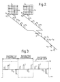
- An electro-optic imaging system comprises an interferometer 1, two detector arrays 2 and associated lenses 3.
- the interferometer is configured as a Twyman-Green interferometer using retro-reflectors 4 rather than plane mirrors.
- One of the retro-reflectors 4 is attached to a piezo-electric cell 5 arranged to drive it reciprocally and so to vary the length of one arm of the interferometer 1.
- light from the scene containing the image which is to be detected together with superimposed clutter is focussed into the interferometer 1 by one of the lenses 3. It passes through the interferometer being split at a beam splitter 6 and recombined before being output from two orthogonal faces of the beam splitter 6. The output light from the two faces is focussed by lenses 3 onto respective photodetector arrays 2.
- One of the two retro-reflectors 4 is positioned so that the optical path lengths for the associated arm of the interferometer differs from that in the other arm of the interferometer by a predetermined distance. This distance is chosen to lie between the characteristic coherence lengths of the image and the clutter.
- the characteristic coherence lengths may be inherently different as when, for example, the object is illuminated by laser light and the clutter is in the form of white light, or alternatively may have been produced by selective filtering of the received optical signal before it reaches the interferometer. In the case of an object illuminated by a He-Ne laser the characteristic coherence length is 30 cm.
- White light clutter by contrast may have a coherence length of typically 1.9 microns.
- the piezo-electric cell 5 drives one of the retro-reflectors 4 repeatedly backwards and forwards.
- the amplitude of the reciprocal movement is chosen according to the requirements of a particular imaging system but is typically less than ⁇ 15 microns.
- the offset path-difference which may be an order of magnitude greater is controlled through a combination of a fine DC bias to the piezo-electric cell 5 and use of a stepper motor attached to the retro-reflector 4 for coarse adjustments, one stepping unit corresponding to 1.25 microns.
- the stepper motor may be interfaced to a local computer.
- the effect of combining an offset path-difference with reciprocal movement of one of the retro-reflectors 4 is to modulate selectively the intensity of the image by virtue of its longer coherence length. Since the clutter has a coherence length less than the offset path-difference it does not interfere to create a fringe system and so its intensity is not modulated by the movement of the retro-reflector 4.
- Antiphase outputs from the interferometer 1 are focussed by lenses 3 onto the photodetector arrays 2.
- the resulting electrical signals are then processed to recover the intensity modulated image from the unmodulated clutter, as shown in Figure 2.
- Signals from corresponding pixels a i , b i of the two detector arrays 2 are fed to a differential amplifier 7.
- the differential amplifier 7 outputs a stream of values dependent upon the difference in intensities of the corresponding pixels a i , b i . For the reasons given in the theoretical discussions below this has the effect of cancelling the DC elements of the received image, that is those elements which are unvarying in intensity.
- the output from the differential amplifier 7 is further processed by multiplication with a reference wave having the same period as the intensity modulation of the image caused by the reciprocal movement of the piezo-electric cell 5.
- the signal is then time averaged as shown in Figure 4. This removes fixed pattern noise caused by different gains of corresponding pixels in the two arrays since this is fixed with time.
- the resulting signal will, in the ideal case, consist solely of the image without clutter or noise and may be output to a suitable display device or stored for further processing.
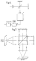
- FIG. 5 An alternative arrangement for signal processing is shown in Figure 5.
- the outputs of the detector arrays 2, which in this case are either vidicon cameras or CCD arrays, are digitised individually by A/D converters and the resulting digitised signals transmitted to a computer 8 for further processing.
- the same computer may be used to control the drive of the piezo-electric cell 5.
- the signals representing the two images are subtracted in a manner precisely analogous to that described above but using processing in the digital rather than analogue domain.
- FIG. 6 An alternative embodiment is illustrated schematically in Figure 6.
- a single vidicon camera or CCD array is used as a detector.
- successive frames from the camera are stored in the image store 9 before being transmitted to the computer 8 for processing.
- the piezo-electric cell 5 moves the retro-reflector 4 by such a distance that the two images are in antiphase.
- the stored digitised images are then processed in the manner described above.
- the function m ( x ) is illustrated in figure 2 for three sources of coherence lengths L B , L S1 and L S2 .
- L S1 and L S2 correspond to the signals to be detected and L B is that associated with the background clutter. If the interferometer has a mean path difference x 0 where: L B ⁇ x 0 ⁇ L S1 (5 a ) or L B ⁇ x 0 ⁇ L S2 (5 b ) then only the signal of interest will produce a significant modulation which can be observed when the mirror is oscillated with a small amplitude about x 0.
- the coherence sensor can be modified to incorporate imaging by using the Twyman-Green configuration shown in Figure 7.
- This is essentially an adaptation of a Michelson interferometer.
- each point source is converted to set of plane waves whose propagation direction is at a particular angle to the optical axis.
- This angular information is then converted back to positional coordinates by L2.
- the input image is related to the output image by where, and f1,f2 are the focal lengths of the lenses shown in Figure 7.
- the output from the imaging system will depend on the arrangement of the mirrors. If they are inclined to each other then the interference pattern will be localised at the mirror plane (fringes of equal thickness or Fizeau fringes). This will, in general, be in a different plane to the scene and the position of the image and interference pattern will not coincide in the Twyman-Green system. The two positions can be made conincidental by imaging the scene at the region of the mirrors. However, this would result in converging light passing through the interferometer and this could lead to severe aberrations of the wavefront by the beamsplitter. If the mirrors are parallel, however, then the interference modulation is localised at infinity (fringes of equal inclination or Hadinger fringes).
- This modulation can be made to coincide with the image in the interferometer.
- the form of the modulation will be similar to that described above but with the important difference that the modulation will occur at the equivalent source position.
- Another disadvantage of using the fringes of equal thickness is that the electronic processing requirements would be more demanding.
- the imaging system envisaged would be based on the fringes of equal inclination.
- One possible type of detector that would be suitable for use in the imaging system is a two dimensional CCD array (figure 8). This would allow a pixel by pixel processing and analysis routine to be used and this could be carried out over a time period that is short compared to the television frame rate. If a digital technique is used, the limiting time factor would be the A/D conversion process which would require between 0.2 N 2 ⁇ s and 2 N 2 ⁇ s.
- the main advantage of processing the signals digitally is that the error in associating the pixels between the arrays is greatly reduced. Since we are no longer dealing with a single element detector, the source size relative to the pixel size must be considered. This can, in fact, lead to an additional degree of control and discrimination in the coherence sensor.
- the system is illustrated in figure 1 . The following is a summary of the possible situations that will be encountered in practise. In these, the equations for the signal to noise ratio assume that the background intensity is much greater than the signal. Also, the background will, in all cases, be assumed to extend throughout the field of
- the shot-noise is given by and the signal is given by
- I B and I S are the background and signal flux levels.
- the signal-to-noise is given by In terms of the S/N of the single detector case we have The signal to clutter ratio remains unchanged. However, the absolute signal level is reduced by a factor of M 2 and this could be a critical factor in cases where the noise is of a non-shot type. For thermal noise the level is independent of the background intensity. The S/N is given by This degradation could be very limiting for the array system.
- the pixel size is the pixel size since this will affect the S/C , S/N , the resolution and the pixel noise.
- the optimisation of the first two factors have been described previously.
- the resolution requirement will be defined by the positional accuracy needed and this will depend on the particular application.
- the pixel or fixed pattern noise is due to differences in outputs between adjacent pixels (for the same incident flux) and is a consequence of the variations in the properties of the silicon substrate. Thus the larger the pixels are, the more these fluctuations are averaged and the smaller the noise becomes.
- a PSD can be incorporated into the imaging system but in order to give an output sensitive to signal position, the electronic processing would necessarily be more complex.
- the processing required is illustrated in figure 2.
- the pixel stream from each image is line feed into a differential amplifier. If the input images are updated at 50 Hz , the output difference image will be modulated at 50 Hz . By multiplying by a wave at 25 Hz (figure 3) the output will be equivalent to that from a demodulator.
- the low-pass filtering or integration stage can be accomplished by either a digital frame storing technique or by directly outputing the differenced signal to a T.V. monitor or array (figure 4). The latter of these is equivalent to time-averaging.
- this procedure would be independent of different pixel gains.
- the system used is illustrated in figure 6.
- the interferometer was set at a fixed path-difference that corresponded to the constructive interference of the signal but which had x 0 » L B . This was recorded on a video tape. Next, the path-difference was changed such that the signal destructively interfered. This was again recorded. By digitally subtracting the two frames, a differenced image was obtained.
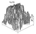
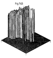
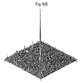
- FIG 12 For this demonstration a laser within a given scene was used. This is shown in figure 12 together with its intensity plot.
- the positional coordinates L,F and R show the correspondence between the two figures.
- the input scene is from the BAe terrain model and shows two tanks passing through a village.
- a He-Ne laser beam has been reflected off the first tank and can be seen to the right of the barrel.
- the image is quite poor a regards resolution. This is due to the high magnification required because of the small input aperture aperture of the interferometer.
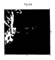
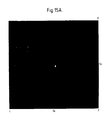
- Figures 13 and 14 show the image with a 50% and 75% threshold level respectively.
- the laser beam can be located by the coordinates S z and S y . It will be noted that even the thresholded images contain a very high level of clutter which would prevent detection.
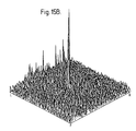
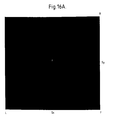
- the difference image is shown in figure 15 together with its intensity distribution.
- the presence of the laser is clearly evident.
- the other spikes are due to a sub-pixel misalignment of the two recorded images prior to differencing and this is a consequence of the poor subtraction method.
- the spikes on the left-hand side of the image correspond to the high contrast edges of the buildings.
- this residual clutter (which is independent of coherence) could be significantly reduced by both accurate alignment of the elements and the use of a PSD.
- This alignment can be achieved by using a telescope in the position of the source which is focussed onto the overlapping images of the array elements.
- a 3 ⁇ 3 averaging matrix was scanned over the intensity plot of the differenced image. The result is shown in figure 17 together with the original plot for comparison.
Landscapes
- Physics & Mathematics (AREA)
- Spectroscopy & Molecular Physics (AREA)
- General Physics & Mathematics (AREA)
- Engineering & Computer Science (AREA)
- Theoretical Computer Science (AREA)
- Mathematical Physics (AREA)
- Nonlinear Science (AREA)
- Optics & Photonics (AREA)
- Instruments For Measurement Of Length By Optical Means (AREA)
Claims (8)
- Verfahren zur Verarbeitung eines optischen Signals, um eine Abbildung aus überlagertem Lärm rückzugewinnen, wobei die Abbildung und der Lärm verschiedene charakteristische Kohäsionslängen haben, wobei das Verfahren umfasst, das empfangene optische Signal auf ein optisches Interferometersystem (1) mit einem Paar Armen (1A,1B) anzuwenden, wobei die Länge eines Armes von der Länge des anderen Armes durch eine Entfernung verschieden ist, die grösser als eine der charakteristischen Kohäsionslängen ist, Weglänge eines Armes (1A,1B) periodisch zu ändern, eine durch die Amplitude modulierte Ausgabe des Interferometersystems (1) bei einer Nachweisanordnung (2) nachzuweisen, und das sich ergebende Signal zu verarbeiten, um das Bild rückzugewinnen, dadurch gekennzeichnet, das Gegenphasenausgaben des Interferometersystems unabhängig nachgewiesen werden, und die sich ergebenden Signale voneinander substrahiert werden, um das Bild rückzugewinnen.
- Verfahren nach Anspruch 1, in dem die Gegenphasenausgaben des Interferometersystems (1) nachgewiesen werden, indem eine erste Ausgabe an einer Nachweisanordnung (2) empfangen wird, die erste Ausgabe gespeichert wird, und nachfolgend eine zweite Ausgabe in Gegenphase zu der ersten Ausgabe an derselben Nachweisanordnung (2) zu empfangen.
- Verfahren nach Anspruch 1, in dem die Gegenphasenausgaben des Interferometersystems (1) nachgewiesen werden, indem entsprechende Nachweisanordnungen (2) an entsprechenden Ausgaben des Paares von Armen (1A,1B) angeordnet werden, und die Gegenphasenausgaben von den Armen (1A,1B) im wesentlichen gleichzeitig empfangen werden.
- Elektrooptisches Abbildungssystem zur Rückgewinnung einer Abbildung aus überlagertem Lärm, wobei die Abbildung und der Lärm verschiedene charakteristische Kohäsionslängen haben, das ein Interferometersystem (1) mit einem Paar von Armen (1A,1B) umfasst, und angeordnet ist, um ein empfangenes optisches Signal zwischen zwei Wegen aufzuspalten, wobei die Weglängen durch eine Entfernung verschieden sind, die grösser als eine der charakeristischen Kohäsionslängen ist, Wegänderungsmittel (5), die angeordnet sind, um die Länge eines der optischen Wege periodisch zu ändern, Abbildungsnachweismittel (2), die angeordnet sind, um eine durch die Amplitude modulierte Ausgabe (1) des Interferometersystems (1) zu empfangen, wobei die Abbildungsnachweismittel (2) wenigstens eine lichtempfindliche Nachweisanordnung einschliessen, und Signalverarbeitungsmittel, die angeordnet sind, um Signale von den Abbildungsnachweismitteln (2) zu verarbeiten, um die Abbildung rückzugewinnen, dadurch gekennzeichnet, dass die Abbildungsnachweismittel (2) angeordnet sind, um Gegenphasenausgaben des Interferometersystems unabhängig nachzuweisen, und die Signalverarbeitungsmittel (7) Subtraktionsmittel einschliessen, die angeordnet sind, um Signale von den Abbildungsnachweismitteln (2), die den Gegenphasenausgaben entsprechen, zu substrahieren.
- Abbildungssystem nach Anspruch 4, in dem die Abbildungsnachweismittel (2) ein Paar lichtempfindliche Nachweisanordnungen umfassen, die angeordnet sind, um Gegenphasenausgaben von entsprechenden Armen des Interferometersystems zu empfangen.
- Abbildungssystem nach Anspruch 4, in dem die Abbildungsnachweismittel (2) eine einzige Videokamera umfassen, und Mittel (8), um eine Abbildungsausgabe in der Kamera zu speichern.
- Abbildungssystem nach einem der Ansprüche 4 bis 6, in dem die Abziehmittel (7) einen Differentialverstärker umfassen, der angeordnet ist, um an seinem Eingang Signale von den Abbildungsnachweismitteln (2), die gleichen Rasterpunkten der Gegenphasenausgaben entsprechen, zu empfangen.
- System nach Anspruch 7, in dem die Verarbeitungsmittel weiterhin Multiplikationsmittel umfassen, die angeordnet sind, um eine Ausgabe von dem Differentialverstärker mit einem festen Frequenzreferenzsignal zu multiplizieren.
Applications Claiming Priority (2)
| Application Number | Priority Date | Filing Date | Title |
|---|---|---|---|
| GB8727446 | 1987-11-24 | ||
| GB878727446A GB8727446D0 (en) | 1987-11-24 | 1987-11-24 | Electro-optic imaging system |
Publications (3)
| Publication Number | Publication Date |
|---|---|
| EP0318288A2 EP0318288A2 (de) | 1989-05-31 |
| EP0318288A3 EP0318288A3 (en) | 1990-05-30 |
| EP0318288B1 true EP0318288B1 (de) | 1993-09-15 |
Family
ID=10627431
Family Applications (1)
| Application Number | Title | Priority Date | Filing Date |
|---|---|---|---|
| EP19880311140 Expired - Lifetime EP0318288B1 (de) | 1987-11-24 | 1988-11-24 | Elektrooptisches Abbildungssystem |
Country Status (3)
| Country | Link |
|---|---|
| EP (1) | EP0318288B1 (de) |
| DE (1) | DE3884149D1 (de) |
| GB (1) | GB8727446D0 (de) |
Families Citing this family (1)
| Publication number | Priority date | Publication date | Assignee | Title |
|---|---|---|---|---|
| WO1995024621A1 (en) * | 1994-03-09 | 1995-09-14 | The Secretary Of State For Defence | Coherence imaging system |
Family Cites Families (1)
| Publication number | Priority date | Publication date | Assignee | Title |
|---|---|---|---|---|
| US4735507A (en) * | 1986-07-11 | 1988-04-05 | The Perkin-Elmer Corporation | Imaging coherent radiometer |
-
1987
- 1987-11-24 GB GB878727446A patent/GB8727446D0/en active Pending
-
1988
- 1988-11-24 DE DE88311140T patent/DE3884149D1/de not_active Expired - Lifetime
- 1988-11-24 EP EP19880311140 patent/EP0318288B1/de not_active Expired - Lifetime
Also Published As
| Publication number | Publication date |
|---|---|
| EP0318288A2 (de) | 1989-05-31 |
| GB8727446D0 (en) | 1988-11-16 |
| EP0318288A3 (en) | 1990-05-30 |
| DE3884149D1 (de) | 1993-10-21 |
Similar Documents
| Publication | Publication Date | Title |
|---|---|---|
| US5418608A (en) | Three dimensional mapping systems and methods | |
| US6229913B1 (en) | Apparatus and methods for determining the three-dimensional shape of an object using active illumination and relative blurring in two-images due to defocus | |
| EP1643210B1 (de) | Verfahren und Vorrichtung zum Messen der Form eines Objekts | |
| US5745226A (en) | Passive optical velocity measurement device and method | |
| US8736847B2 (en) | Method and apparatus for imaging | |
| US20010052985A1 (en) | Image capturing apparatus and distance measuring method | |
| US5708498A (en) | Three dimensional color imaging | |
| US11119193B2 (en) | Micro resolution imaging range sensor system | |
| US3708619A (en) | Automatic focusing of optical systems | |
| US5350911A (en) | Wavefront error estimation derived from observation of arbitrary unknown extended scenes | |
| Mundy et al. | A three-dimensional sensor based on structured light | |
| JP4015724B2 (ja) | コヒーレント重畳受信中における2光波のアライメント制御のための方法および装置 | |
| US3921080A (en) | Analog data processor | |
| US4037958A (en) | Apparatus for determining photoelectrically the position of at least one focusing plane of an image | |
| EP0882211B1 (de) | Verfahren und apparat zur reduzierung von unerwünschten rauscheffekten in einem dreidimensionalen farbbilderzeugungssystem | |
| EP0318288B1 (de) | Elektrooptisches Abbildungssystem | |
| US12366824B2 (en) | Differential holography | |
| RU2055371C1 (ru) | Адаптивный телескоп | |
| US10215833B1 (en) | Two-axis interferometric tracking utilizing pairs of shearing interferometers | |
| CA1079955A (en) | Method of determining parallax effects in a stereoscopic optical system | |
| RU2020522C1 (ru) | Адаптивный телескоп | |
| JP2001304966A (ja) | フーリエ分光画像計測装置及びこれを用いた人工衛星 | |
| JP2000329514A (ja) | 干渉縞画像の補正方法 | |
| JP4125563B2 (ja) | 光学素子位置計測方法及び装置、導波路調整方法及び装置ならびに光モジュール製造方法 | |
| JP2000121332A (ja) | 三次元形状測定装置 |
Legal Events
| Date | Code | Title | Description |
|---|---|---|---|
| PUAI | Public reference made under article 153(3) epc to a published international application that has entered the european phase |
Free format text: ORIGINAL CODE: 0009012 |
|
| AK | Designated contracting states |
Kind code of ref document: A2 Designated state(s): BE DE FR GB NL |
|
| PUAL | Search report despatched |
Free format text: ORIGINAL CODE: 0009013 |
|
| AK | Designated contracting states |
Kind code of ref document: A3 Designated state(s): BE DE FR GB NL |
|
| 17P | Request for examination filed |
Effective date: 19901109 |
|
| 17Q | First examination report despatched |
Effective date: 19920603 |
|
| RAP3 | Party data changed (applicant data changed or rights of an application transferred) |
Owner name: BRITISH AEROSPACE PUBLIC LIMITED COMPANY |
|
| GRAA | (expected) grant |
Free format text: ORIGINAL CODE: 0009210 |
|
| AK | Designated contracting states |
Kind code of ref document: B1 Designated state(s): BE DE FR GB NL |
|
| PG25 | Lapsed in a contracting state [announced via postgrant information from national office to epo] |
Ref country code: NL Effective date: 19930915 Ref country code: FR Effective date: 19930915 Ref country code: DE Effective date: 19930915 Ref country code: BE Effective date: 19930915 |
|
| REF | Corresponds to: |
Ref document number: 3884149 Country of ref document: DE Date of ref document: 19931021 |
|
| EN | Fr: translation not filed | ||
| NLV1 | Nl: lapsed or annulled due to failure to fulfill the requirements of art. 29p and 29m of the patents act | ||
| PLBE | No opposition filed within time limit |
Free format text: ORIGINAL CODE: 0009261 |
|
| STAA | Information on the status of an ep patent application or granted ep patent |
Free format text: STATUS: NO OPPOSITION FILED WITHIN TIME LIMIT |
|
| 26N | No opposition filed | ||
| REG | Reference to a national code |
Ref country code: GB Ref legal event code: 732E |
|
| PGFP | Annual fee paid to national office [announced via postgrant information from national office to epo] |
Ref country code: GB Payment date: 19981020 Year of fee payment: 11 |
|
| PG25 | Lapsed in a contracting state [announced via postgrant information from national office to epo] |
Ref country code: GB Free format text: LAPSE BECAUSE OF NON-PAYMENT OF DUE FEES Effective date: 19991124 |
|
| GBPC | Gb: european patent ceased through non-payment of renewal fee |
Effective date: 19991124 |