EP0318270B1 - A multiprocessor system and corresponding method - Google Patents
A multiprocessor system and corresponding method Download PDFInfo
- Publication number
- EP0318270B1 EP0318270B1 EP19880311089 EP88311089A EP0318270B1 EP 0318270 B1 EP0318270 B1 EP 0318270B1 EP 19880311089 EP19880311089 EP 19880311089 EP 88311089 A EP88311089 A EP 88311089A EP 0318270 B1 EP0318270 B1 EP 0318270B1
- Authority
- EP
- European Patent Office
- Prior art keywords
- cluster
- order
- processors
- control unit
- cpu1
- Prior art date
- Legal status (The legal status is an assumption and is not a legal conclusion. Google has not performed a legal analysis and makes no representation as to the accuracy of the status listed.)
- Expired - Lifetime
Links
Images


Classifications
-
- G—PHYSICS
- G06—COMPUTING; CALCULATING OR COUNTING
- G06F—ELECTRIC DIGITAL DATA PROCESSING
- G06F15/00—Digital computers in general; Data processing equipment in general
- G06F15/16—Combinations of two or more digital computers each having at least an arithmetic unit, a program unit and a register, e.g. for a simultaneous processing of several programs
- G06F15/177—Initialisation or configuration control
-
- G—PHYSICS
- G06—COMPUTING; CALCULATING OR COUNTING
- G06F—ELECTRIC DIGITAL DATA PROCESSING
- G06F15/00—Digital computers in general; Data processing equipment in general
- G06F15/16—Combinations of two or more digital computers each having at least an arithmetic unit, a program unit and a register, e.g. for a simultaneous processing of several programs
- G06F15/163—Interprocessor communication
-
- G—PHYSICS
- G06—COMPUTING; CALCULATING OR COUNTING
- G06F—ELECTRIC DIGITAL DATA PROCESSING
- G06F15/00—Digital computers in general; Data processing equipment in general
- G06F15/76—Architectures of general purpose stored program computers
- G06F15/80—Architectures of general purpose stored program computers comprising an array of processing units with common control, e.g. single instruction multiple data processors
- G06F15/8007—Architectures of general purpose stored program computers comprising an array of processing units with common control, e.g. single instruction multiple data processors single instruction multiple data [SIMD] multiprocessors
- G06F15/8015—One dimensional arrays, e.g. rings, linear arrays, buses
Definitions
- the present invention relates to a multiprocessor system, more particularly, it relates to a method and an apparatus for control of processors constituting the multi-processor system.
- each processor is associated with a shared memory.
- the shared memory is connected to a system bus, to which a master controller is also connected.
- a master controller is also connected.
- data from an originating processor is stored in its shared memory. This is accessed by the master controller, which then enables the shared memory of any processors to which the data must be transmitted, and simultaneously writes the data to each such shared mamory.
- a processor can resume operations as soon as data is stored in its associated memory, with no need to wait until the data reaches its destination. Further, data may simultaneously be transmitted to a plurality of destination processors. Nevertheless, every data transfer must be effected via the shared memories and master controller. This may be time consuming.
- EP-A-0110569 discloses a ring network in which processors are divided into clusters. The transmission of data around the ring network is controlled such that the data will not be transmitted between adjacent nodes if a buffer associated with one node becomes full.
- the present invention is advantageous for a large scale numerical simulation in scientific and technical fields in which high speed calculations are necessary.
- a method of control between processors constituting a multiprocessor system comprises the steps as set out in claim 1.
- each cluster is an element for processing the access control of the processors. This enables high speed processing of orders between processors and a simplification of a control program.
- an apparatus for a cluster control between processors constituting a multiprocessor system, the processors being divided into a plurality of clusters comprises:
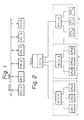
- FIG. 1 is a schematic block diagram of a conventional multiprocessor system.
- the multi-processor system is constituted by, for example, processors CPUO to CPU5, and each processor is connected in parallel to another processor through a bus line BUS and a mutual control is carried out between one processor and the other.
- each processor is set to four states having an exclusive relationship therebetween; i.e., any one of four states ("STOP ⁇ , "OPERATION”, “LOAD” and "CHECK-STOP") are set in each processor.
- STOP ⁇ , "OPERATION”, "LOAD” and "CHECK-STOP” are set in each processor.
- one processor When carrying out an access, one processor outputs a sense signal to the other processor, to recognize the state of other processor, receives a response from the other processor involving the above four states, and carries out a mutual control in accordance with the above four states.
- FIG. 2 is a basic block diagram of an apparatus for the cluster control in the multiprocessor system according to the present invention.
- a plurality of processors CPU1 to CPUn are divided into “m" groups ( 1 to m) each having three processors, and each group is called a "cluster”.
- MCU1 to MCUm are a memory control unit provided in each cluster and connected between the processor and a global control unit GCU.
- the global control unit GCU controls the access between clusters, as explained in detail hereinafter, and is contained in a global storage unit GSU.
- the state of each cluster is defined by the global control unit GCU based on the state of the processors belonging to that cluster. Further, the global control unit GCU sets up an order for each cluster and controls the processor, based on the order for each cluster, through the memory control unit MCU.
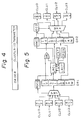
- FIG. 3 is a schematic block diagram of a cluster according to an embodiment of the present invention.
- the multiprocessor system is constituted by sixty four processors, which are divided into sixteen clusters each having four processors CPU0 to CPU3. Therefore, the global control unit GCU controls only sixteen clusters 0 to 15 through the bus line BUS.
- each cluster has the same structure.
- the cluster 0 comprises a memory control unit MCU, four processors CPU0 to CPU3, a local storage unit LSU, a direct access storage device DASD, a service processor SVP, an input/output processor IOP, and a channel element CHE connected between the MCU and the DASD.
- the global control unit GCU is used in common for all clusters 0 to 15, and is connected to each cluster through the bus line BUS.
- the processor belonging to each cluster is defined by the four states "STOP”, “OPERATION”, “LOAD”, and "CHECK-STOP", and these four states are exclusive therebetween and change under the following conditions.
- the state of the cluster is based on the state of the processors belonging to that cluster, as follows.
- None of the processors in the cluster is in the OPERATION or LOAD state, and at least one processor in the cluster is in the STOP state.
- CLUSTER-CHECK-STOP further includes the states wherein the processors are not connected to each other or none of the processors is supplied with power.
- the cluster When a channel subsystem damage is found in the cluster, the cluster is placed in the SUBSYSTEM-DAMAGE state.
- the SUBSYSTEM-DAMAGE state When the SUBSYSTEM-DAMAGE state is set, the CLUSTER-STOP Or CLUSTER-CHECK-STOP states are simultaneously set in the cluster.
- Three main orders are sent to each cluster, as defined as follows. Namely, the CLUSTER-SENSE order, the CLUSTER-SYNCHRONOUS-CALL order (floating interruption order), and the CLUSTER-RESET and LOAD order (RESET and IPL order). Further, for example, the CLUSTER-BROADCAST-INTERRUPTION order for accessing the same order to all clusters and CLUSTER-ASYNCHRONOUS-INTERRUPTION order are sent, and these orders are shown as a whole as a GSIGP order.
- the GSIGP order is mainly used for a floating interruption between the processors, as explained hereinafter.
- Fig. 3 the encircled numbers correspond to the following steps. The flowchart of these steps is shown in Figs. 7A and 7B.
- the global control unit GCU returns the GSIGP order including the incorrect destination to the memory control unit MCU at the transmission side in the same order as the GSIGP order sent from other cluster. In this case, a flag bit indicating the incorrect destination is added to the order.
- the memory control unit MCU at the transmission side recognizes the flag bit in the GSIGP order received, the MCU returns the same GSIGP order as above to the global control unit GCU as the status information. At that time, the content of the GSIGP order is ignored.
- the global control unit GCU sends the returned status information to the memory control unit MCU at the transmission side as the status information, also the status information received from the destination side in the case of a normal GSIGP order.
- the interface lines between the MCU and the GCU include a signal line for discriminating either the status information or the order from the transferred information.
- the GSIGP order is sent to the memory control unit MCU as the order and that order is returned to the global control unit GCU, and then that order is again returned to the memory control unit MCU as the status information. This is because these procedures make the operation procedures at the GCU and the MCU almost identical.
- step 5 Since the procedures from step 1 to step 5 are the same as for the steps shown in Fig. 7, an explanation thereof is omitted. The following step follows step 5.
- the memory control unit MCU of the reception side interprets the CLUSTER-SYNCHRONOUS-CALL order, it determines whether an interruption pending latch of that memory control unit MCU is turned ON or not.
- the memory control unit MCU writes the "turned ON state" to the status information.
- the interruption pending latch of the memory control unit MCU is turned ON as shown by steps 6′-1 and 6′-2.
- step 7 to step are carried out after the above step 6′. Further, when the interruption enabled processor exists in the cluster at the reception side, the interruption is made to that processor.
- step 5 Since the procedures from the step 1 to the step 5 are the same as for the steps shown in Fig. 7, an explanation thereof is omitted. The following step follows step 5
- the memory control unit MCU at the reception side interprets the CLUSTER-RESET and IPL order, and requests that these orders be processed by the service processor SVP in that cluster.
- the memory control unit MCU stores the status information. The following procedures are the same as for step 7 to step shown in Fig. 7.
- the service processor SVP at the reception side resets all devices in the cluster, starts an IPL (Initial Program Loading) operation, and writes the program from the direct access storage device DASD to the local storage unit LSU.
- IPL Initial Program Loading
- the IPL operation is performed asynchronously to the termination of the order at the transmission side, as shown by step , the IPL operation is not always terminated in the reception side even if the order at the transmission side is terminated.
- FIG. 5 is a schematic block diagram of a global control unit according to an embodiment of the present invention.
- the global control unit GCU is an essential part of the global storage unit GSU.
- RCV represents a receiver, PRT a priority circuit, LRCL a logical-to-real cluster translation logic circuit, LRCT a logical-to-real cluster translation table, CCNT a cluster connecting table, COPN a cluster power-on table, MPX a multiplexer, ECD an encoder, OR an order, and DRV a driver.
- the order OR1 comprises a CLUSTER-INVALID (IV), a LOGICAL-CLUSTER-ID (LDI), a command (COM) and a parameter (PRM). Further, the order OR2 comprises a LOGICAL-DRIVE-CLUSTER-ID (LDCI) instead of the LOGICAL-CLUSTER-ID (LCI), RDCI is a REAL-DRIVE-CLUSTER-ID and RRCI is a REAL-RECEIVE-CLUSTER-ID.
- IV CLUSTER-INVALID
- LCI LOGICAL-CLUSTER-ID
- COM command
- PRM parameter
- the order OR2 comprises a LOGICAL-DRIVE-CLUSTER-ID (LDCI) instead of the LOGICAL-CLUSTER-ID (LCI)
- RDCI is a REAL-DRIVE-CLUSTER-ID
- RRCI is a REAL-RECEIVE-CLUSTER-ID.
- the cluster connecting table CCNT indicates the state of connection of the cluster; the command COM designates the order of the GSIGP; the cluster power-on table CPON indicates a power-on/off state of the cluster; the driver DRV transfers the order to the cluster; and, the encoder ECD encodes the IV bit and the RRCI bit and determines the destination of the processor transferring the command.
- the bit IV indicates the invalidity of the cluster, and is normally "0" when generating the command request and turned ON when the designated cluster does not exist or the power is not turned ON;
- the bit LCI is a logical identifier and the target of the request is designated by the logical cluster number; and the bit LDCI is a logical processor number of the processor generating the request and sets the output of the table LRCL.
- the circuit LRCL is a logical block converting a logical cluster number to a physical cluster number.
- the circuit LRCL inputs the bit LCI and outputs the bit RRCI by referring to the table LRCT.
- the circuit LRCL checks whether or not the designated real cluster is connected (command CCNT) and the power of the designated real cluster is turned ON. If the designated cluster is incorrect, the bit IV is turned ON. Further, the circuit LRCL converts the bit RDCI to the bit LDCL.
- the table LRCT refers to the relationship between the logical cluster number and the physical cluster number.
- the multiplexer MPX selects the cluster generating the request.
- the parameter PRM is an order of the GSIGP and the order necessitating the parameter is transferred through the PRM.
- the priority circuit PRT determines the cluster competition state and gives the priority right to the request.
- the receiver RCV receives the requests from the cluster CLU0 to CLU3.
- the bit RDCI is a real cluster number which generated the request and is set by the output of the priority circuit PRT.
- the bit RRCI is a register indicating the destination of the cluster transferring the request and is set by the output of the circuit LRCL.
- FIG. 6 is a schematic block diagram of the memory control unit MCU according to an embodiment of the present invention.
- GORV represents a GSIGP order receiver, SCGE a states and condition code generator, GARV a GSIGP acknowledge receiver, GRDV a GSIGP request driver, GRRV a GSIGP request receiver, COEX a command executor, ITPL an interruption pending latch, IOP an I/0 processor, SGE a status generator, and GADV a GSIGP acknowledge driver.
- the GSIGP acknowledge receiver GARV is a circuit receiving the acknowledge ACK from the global control unit GCU;
- the status and condition code generator SCGE is a circuit generating the STATUS and CC order based on the acknowledge ACK;
- the GSIGP request drive is a circuit generating the request of the GSIGP to the GCU;
- the priority circuit PRT is a circuit determining the priority of the request when sent from the processor CPU;
- the GSIGP order receiver GORV is a circuit receiving the GSIGP request from the processor CPU and generating the request to the global control unit GCU; and the command executor COEX executes the request sent from the GCU through the GSIGP request receiver GRRV.
- the command executor COEX requests the status generator SGE to generate the status information
- the command executor COEX requests the service processor SVP to generate the status information and requests the status generator SGE to also generate the status information.
- the command executor COEX checks the state of the interruption pending latch ITPL. If the interruption pending latch ITPL is turned 0FF, the command executor COEX turns ON the interruption pending latch ITPL and informs the status generator SGE that the ITPL is turned ON. If the interruption pending latch ITPL is turned ON, the command executor COEX informs the status generator SGE that the ITPL is turned ON.
- the interruption pending latch ITPL is turned ON by the request from the command executor COEX. Further, the interruption pending latch ITPL supervises the interruption mask MSK to inhibit the interruption from the processor CPU, detects the processor CPU for which the interrupt mask is turned ON, and derives the interrupt from that processor.
- the I/O processor IOP carries out the input/output processing. When a fault occurs at the I/O processor IOP, a SUBSYSTEM-DAMAGE signal is sent to the status generator SGE.
- the service processor SVP carries out the reset of the cluster and the IPL processing. Further, the service processor SVP processes the operator function.
- the status generator SGE generates the status information in accordance with the request from the command executor COEX, and further, takes in the information sent from the service processor SVP and the I/O processor IOP.
- the GSIGP request receiver GRRV receives the GSIGP request from the global control unit GCU, and the GSIGP acknowledge driver GADV returns the generated status information to the cluster which generated the command.
Description
- The present invention relates to a multiprocessor system, more particularly, it relates to a method and an apparatus for control of processors constituting the multi-processor system.
- In data processing systems, it has been found to be advantageous to provide a plurality of processors to increase the overall speed of the system. Various control methods and system architectures have been developed to optimise the speed of such processing systems, in particular to optimise the speed for data communication between the processors. One system is disclosed in GB-A-2112186. Accordingly to the disclosure in this application, each processor is associated with a shared memory. The shared memory is connected to a system bus, to which a master controller is also connected. When a data transfer is required, data from an originating processor is stored in its shared memory. This is accessed by the master controller, which then enables the shared memory of any processors to which the data must be transmitted, and simultaneously writes the data to each such shared mamory. With this system, a processor can resume operations as soon as data is stored in its associated memory, with no need to wait until the data reaches its destination. Further, data may simultaneously be transmitted to a plurality of destination processors. Nevertheless, every data transfer must be effected via the shared memories and master controller. This may be time consuming.
- EP-A-0110569 discloses a ring network in which processors are divided into clusters. The transmission of data around the ring network is controlled such that the data will not be transmitted between adjacent nodes if a buffer associated with one node becomes full.
- The present invention is advantageous for a large scale numerical simulation in scientific and technical fields in which high speed calculations are necessary.
- According to a first aspect of this invention a method of control between processors constituting a multiprocessor system comprises the steps as set out in
claim 1. - By dividing the multiprocessor system constituted by a plurality of processors into a plurality of groups, each of which is called a "cluster", the control of access between the processors is performed through each cluster. Thus each cluster is an element for processing the access control of the processors. This enables high speed processing of orders between processors and a simplification of a control program.
- According to a second aspect of this invention an apparatus for a cluster control between processors constituting a multiprocessor system, the processors being divided into a plurality of clusters, comprises:
- a global control unit connected to each of the clusters through a corresponding bus line for processing an order between the clusters, characterised in that the global control unit comprises a priority circuit for determining a priority of the order sent from each of the clusters, a logical-to-real cluster translation logic circuit for converting a logical cluster number to a physical cluster number, a logical- to-real cluster translation table for referring to a relationship between the logical cluster number and the physical cluster number, a cluster connection table for indicating a connection state of the cluster, and a cluster power-ON table for indicating a power ON/OFF state of the cluster, and
- a memory control unit provided in each of the clusters and connected between the global control unit and each of the processors belonging to each of the clusters and controlling transmission and reception of orders between the global control unit (GCU) and the processors, wherein each of the clusters further comprises a local storage unit connected to the memory control unit and storing data, a direct access storage device connected to the memory control unit and storing data, and a service processor connected to the memory control unit and processing the reset operation and an initial program loading operation, the memory control unit comprises a priority circuit for determining a priority of requests sent from the processors a command executor for executing a request sent from the global control unit, a status generator for generating status information in accordance with a request from the command executor, and an interruption pending latch circuit for turning ON an interruption pending latch.
- An embodiment of a method and apparatus in accordance with this invention will now be described and contrasted with the prior art with reference to the accompanying drawings; in which:-
- Figure 1 is a schematic block diagram of a conventional multiprocessor system;
- Figure 2 is a basic block diagram of an apparatus for a cluster control in the multiprocessor system according to the present invention;
- Figure 3 is a schematic block diagram of a cluster according to an embodiment of the present invention;
- Figure 4 is one example of format of an order according to the present invention;
- Figure 5 is a schematic block diagram of a global control unit according to an embodiment of the present invention;
- Figure 6 is a schematic block diagram of a memory control unit according to an embodiment of the present invention;
- Figure 7 is a flowchart for explaining a CLUSTER-SENSE order according to an embodiment of the present invention;
- Figure 8 is a flowchart for explaining a SYNCHRONOUS-CALL order according to an embodiment of the present invention; and,
- Fig. 9 is a flowchart for explaining a CLUSTER-RESET and IPL order according to an embodiment of the present invention.
- Before describing the preferred embodiments, an explanation will be given of a conventional multi-processor system.
- Figure 1 is a schematic block diagram of a conventional multiprocessor system. In Fig. 1, the multi-processor system is constituted by, for example, processors CPUO to CPU5, and each processor is connected in parallel to another processor through a bus line BUS and a mutual control is carried out between one processor and the other.
- In this multiprocessor system, each processor is set to four states having an exclusive relationship therebetween; i.e., any one of four states ("STOP˝, "OPERATION", "LOAD" and "CHECK-STOP") are set in each processor. When carrying out an access, one processor outputs a sense signal to the other processor, to recognize the state of other processor, receives a response from the other processor involving the above four states, and carries out a mutual control in accordance with the above four states.
- In this system, however, much time is necessary for the management of access steps between the processors, and thus it is difficult to achieve a high speed processing in the multiprocessor system. Further, the control program is complicated due to the large number of access steps.
- Figure 2 is a basic block diagram of an apparatus for the cluster control in the multiprocessor system according to the present invention. In Fig. 2, a plurality of processors CPU1 to CPUn are divided into "m" groups ( 1 to m) each having three processors, and each group is called a "cluster". MCU1 to MCUm are a memory control unit provided in each cluster and connected between the processor and a global control unit GCU. The global control unit GCU controls the access between clusters, as explained in detail hereinafter, and is contained in a global storage unit GSU. The state of each cluster is defined by the global control unit GCU based on the state of the processors belonging to that cluster. Further, the global control unit GCU sets up an order for each cluster and controls the processor, based on the order for each cluster, through the memory control unit MCU.
- In the above structure, since the access between processors is controlled through the cluster, it is possible to reduce the control time between processors. Further, it is possible to simplify the control program since the access is performed between clusters.
- Figure 3 is a schematic block diagram of a cluster according to an embodiment of the present invention. In Fig. 3, the multiprocessor system is constituted by sixty four processors, which are divided into sixteen clusters each having four processors CPU0 to CPU3. Therefore, the global control unit GCU controls only sixteen clusters 0 to 15 through the bus line BUS. In this case, each cluster has the same structure. For example, the cluster 0 comprises a memory control unit MCU, four processors CPU0 to CPU3, a local storage unit LSU, a direct access storage device DASD, a service processor SVP, an input/output processor IOP, and a channel element CHE connected between the MCU and the DASD. The global control unit GCU is used in common for all clusters 0 to 15, and is connected to each cluster through the bus line BUS.
- The processor belonging to each cluster is defined by the four states "STOP", "OPERATION", "LOAD", and "CHECK-STOP", and these four states are exclusive therebetween and change under the following conditions.
- (1) When an operator uses an operating facility.
- (2) When the processor receives a specified "SIGNAL-PROCESSOR (SIGP)" order for that processor.
- (3) When the cluster having that processor receives a specified "GLOBAL SIGNAL PROCESSOR (GSIGP)" order for that cluster.
- Further, the state of the cluster is based on the state of the processors belonging to that cluster, as follows.
- None of the processors in the cluster is in the OPERATION or LOAD state, and at least one processor in the cluster is in the STOP state.
- None of the processors is in the STOP, OPERATION or LOAD states. CLUSTER-CHECK-STOP further includes the states wherein the processors are not connected to each other or none of the processors is supplied with power.
- When a channel subsystem damage is found in the cluster, the cluster is placed in the SUBSYSTEM-DAMAGE state. When the SUBSYSTEM-DAMAGE state is set, the CLUSTER-STOP Or CLUSTER-CHECK-STOP states are simultaneously set in the cluster.
- In this embodiment, when one processor commands another processor to process an order, the command is sent to the cluster to which the other processor belongs and is not sent directly to the other processor.
- Three main orders are sent to each cluster, as defined as follows. Namely, the CLUSTER-SENSE order, the CLUSTER-SYNCHRONOUS-CALL order (floating interruption order), and the CLUSTER-RESET and LOAD order (RESET and IPL order). Further, for example, the CLUSTER-BROADCAST-INTERRUPTION order for accessing the same order to all clusters and CLUSTER-ASYNCHRONOUS-INTERRUPTION order are sent, and these orders are shown as a whole as a GSIGP order. The GSIGP order is mainly used for a floating interruption between the processors, as explained hereinafter.
- The operation of these orders is explained in detail hereinafter.
- In Fig. 3, the encircled numbers correspond to the following steps. The flowchart of these steps is shown in Figs. 7A and 7B.
- ① The processor 1 (CPU1) in the cluster 0 decodes and recognizes the GSIGP order.
- ② The
processor 1 sends the GSIGP order to the memory control unit MCU. The GSIGP order includes a CLUSTER-ID portion and an ORDER portion. - ③ The memory control unit MCU sends the GSIGP order to the global control unit GCU. The GSIGP order includes a SENSE order, a CLUSTER-ID and a parameter, as shown in Fig. 4.
- ④ The global control unit GCU interprets the CLUSTER-ID. When the correct cluster (connected to the cluster) is designated, the flow proceeds to the next step. When the designated cluster is incorrect, the GSIGP order is returned to the cluster at the transmission side with the information "incorrect destination".
- ⑤ The global control unit GCU sends the GSIGP order to the memory control unit MCU of the target cluster.
- ⑥ When the memory control unit MCU at the reception side interprets the SENSE order, it generates the state of that cluster as the status information based on the states of the processors, the information from the input/output processor IOP, and the states of the synchronous call (floating interruption order) in the MCU.
- ⑦ The memory control unit MCU in the cluster at the reception side sends the status information of that cluster to the global control unit GCU.
- ⑧ The global control unit GCU sends the received status information to the memory control unit MCU in the cluster at the transmission side.
- ⑨ The memory control unit MCU sends the received status information and a condition code (CC) to the processor CPU1 which generated the GSIGP order.
- When the processor CPU1 receives the status information and the condition code CC, it interprets this as a termination of the GSIGP order, and proceeds to the next order.

- In the case of an "incorrect destination" mentioned in
step ④, as shown in steps ④-1, ④-2 and ④-3, the global control unit GCU returns the GSIGP order including the incorrect destination to the memory control unit MCU at the transmission side in the same order as the GSIGP order sent from other cluster. In this case, a flag bit indicating the incorrect destination is added to the order. When the memory control unit MCU at the transmission side recognizes the flag bit in the GSIGP order received, the MCU returns the same GSIGP order as above to the global control unit GCU as the status information. At that time, the content of the GSIGP order is ignored. The global control unit GCU sends the returned status information to the memory control unit MCU at the transmission side as the status information, also the status information received from the destination side in the case of a normal GSIGP order. The interface lines between the MCU and the GCU include a signal line for discriminating either the status information or the order from the transferred information. As explained above, in the case of an incorrect destination, the GSIGP order is sent to the memory control unit MCU as the order and that order is returned to the global control unit GCU, and then that order is again returned to the memory control unit MCU as the status information. This is because these procedures make the operation procedures at the GCU and the MCU almost identical. - This step is shown in Fig. 8.
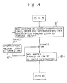
- Since the procedures from
step ① to step ⑤ are the same as for the steps shown in Fig. 7, an explanation thereof is omitted. The following step followsstep ⑤. - ⑥′ When the memory control unit MCU of the reception side interprets the CLUSTER-SYNCHRONOUS-CALL order, it determines whether an interruption pending latch of that memory control unit MCU is turned ON or not. When the latch is turned ON, the memory control unit MCU writes the "turned ON state" to the status information. When the latch is turned 0FF, the interruption pending latch of the memory control unit MCU is turned ON as shown by
steps ⑥′-1 and ⑥′-2. - The same procedures as for
step ⑦ to stepare carried out after theabove step ⑥′. Further, when the interruption enabled processor exists in the cluster at the reception side, the interruption is made to that processor. - The procedures of the CLUSTER-RESET and IPL order are as follows.
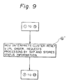
- This step is shown in Fig. 9.
- Since the procedures from the
step 1 to thestep ⑤ are the same as for the steps shown in Fig. 7, an explanation thereof is omitted. The following step followsstep ⑤ - ⑥˝ The memory control unit MCU at the reception side interprets the CLUSTER-RESET and IPL order, and requests that these orders be processed by the service processor SVP in that cluster. When the transmission of information from the memory control unit MCU to the service processor SVP is completed, the memory control unit MCU stores the status information. The following procedures are the same as for
step ⑦ to stepshown in Fig. 7. - The service processor SVP at the reception side resets all devices in the cluster, starts an IPL (Initial Program Loading) operation, and writes the program from the direct access storage device DASD to the local storage unit LSU.
- In this case, since the IPL operation is performed asynchronously to the termination of the order at the transmission side, as shown by step, the IPL operation is not always terminated in the reception side even if the order at the transmission side is terminated.
- Figure 5 is a schematic block diagram of a global control unit according to an embodiment of the present invention. The global control unit GCU is an essential part of the global storage unit GSU. In Fig. 5, RCV represents a receiver, PRT a priority circuit, LRCL a logical-to-real cluster translation logic circuit, LRCT a logical-to-real cluster translation table, CCNT a cluster connecting table, COPN a cluster power-on table, MPX a multiplexer, ECD an encoder, OR an order, and DRV a driver.
- The order OR1 comprises a CLUSTER-INVALID (IV), a LOGICAL-CLUSTER-ID (LDI), a command (COM) and a parameter (PRM). Further, the order OR2 comprises a LOGICAL-DRIVE-CLUSTER-ID (LDCI) instead of the LOGICAL-CLUSTER-ID (LCI), RDCI is a REAL-DRIVE-CLUSTER-ID and RRCI is a REAL-RECEIVE-CLUSTER-ID.
- The cluster connecting table CCNT indicates the state of connection of the cluster; the command COM designates the order of the GSIGP; the cluster power-on table CPON indicates a power-on/off state of the cluster; the driver DRV transfers the order to the cluster; and, the encoder ECD encodes the IV bit and the RRCI bit and determines the destination of the processor transferring the command. The bit IV indicates the invalidity of the cluster, and is normally "0" when generating the command request and turned ON when the designated cluster does not exist or the power is not turned ON; the bit LCI is a logical identifier and the target of the request is designated by the logical cluster number; and the bit LDCI is a logical processor number of the processor generating the request and sets the output of the table LRCL.
- The circuit LRCL is a logical block converting a logical cluster number to a physical cluster number. The circuit LRCL inputs the bit LCI and outputs the bit RRCI by referring to the table LRCT. In the conversion, the circuit LRCL checks whether or not the designated real cluster is connected (command CCNT) and the power of the designated real cluster is turned ON. If the designated cluster is incorrect, the bit IV is turned ON. Further, the circuit LRCL converts the bit RDCI to the bit LDCL.
- The table LRCT refers to the relationship between the logical cluster number and the physical cluster number. The multiplexer MPX selects the cluster generating the request. The parameter PRM is an order of the GSIGP and the order necessitating the parameter is transferred through the PRM. The priority circuit PRT determines the cluster competition state and gives the priority right to the request. The receiver RCV receives the requests from the cluster CLU0 to CLU3. The bit RDCI is a real cluster number which generated the request and is set by the output of the priority circuit PRT. The bit RRCI is a register indicating the destination of the cluster transferring the request and is set by the output of the circuit LRCL.
- Figure 6 is a schematic block diagram of the memory control unit MCU according to an embodiment of the present invention. In Fig. 6, GORV represents a GSIGP order receiver, SCGE a states and condition code generator, GARV a GSIGP acknowledge receiver, GRDV a GSIGP request driver, GRRV a GSIGP request receiver, COEX a command executor, ITPL an interruption pending latch, IOP an I/0 processor, SGE a status generator, and GADV a GSIGP acknowledge driver.
- The GSIGP acknowledge receiver GARV is a circuit receiving the acknowledge ACK from the global control unit GCU; the status and condition code generator SCGE is a circuit generating the STATUS and CC order based on the acknowledge ACK; the GSIGP request drive is a circuit generating the request of the GSIGP to the GCU; the priority circuit PRT is a circuit determining the priority of the request when sent from the processor CPU; the GSIGP order receiver GORV is a circuit receiving the GSIGP request from the processor CPU and generating the request to the global control unit GCU; and the command executor COEX executes the request sent from the GCU through the GSIGP request receiver GRRV. In the SENSE order, the command executor COEX requests the status generator SGE to generate the status information, and in the reset and IPL order, the command executor COEX requests the service processor SVP to generate the status information and requests the status generator SGE to also generate the status information. In the case of an interruption, the command executor COEX checks the state of the interruption pending latch ITPL. If the interruption pending latch ITPL is turned 0FF, the command executor COEX turns ON the interruption pending latch ITPL and informs the status generator SGE that the ITPL is turned ON. If the interruption pending latch ITPL is turned ON, the command executor COEX informs the status generator SGE that the ITPL is turned ON.
- The interruption pending latch ITPL is turned ON by the request from the command executor COEX. Further, the interruption pending latch ITPL supervises the interruption mask MSK to inhibit the interruption from the processor CPU, detects the processor CPU for which the interrupt mask is turned ON, and derives the interrupt from that processor. The I/O processor IOP carries out the input/output processing. When a fault occurs at the I/O processor IOP, a SUBSYSTEM-DAMAGE signal is sent to the status generator SGE. The service processor SVP carries out the reset of the cluster and the IPL processing. Further, the service processor SVP processes the operator function. The status generator SGE generates the status information in accordance with the request from the command executor COEX, and further, takes in the information sent from the service processor SVP and the I/O processor IOP. The GSIGP request receiver GRRV receives the GSIGP request from the global control unit GCU, and the GSIGP acknowledge driver GADV returns the generated status information to the cluster which generated the command.
Claims (7)
- A method of control between processors (CPU1,...,CPUn) constituting a multiprocessor system comprising the steps of:dividing a plurality of processors (CPU1,...,CPUn) constituting the multiprocessor system into a plurality of clusters (1,2,...,m);defining a state of a cluster (1,2,...,m) based on the states of the processors (CPU1,CPU2,CPU3) belonging to that cluster (1,2,...,m);sending an order to that cluster; and,controlling a processor belonging to that cluster based on the order to that cluster,characterised in that each processor (CPU1,...,CPUn) is defined by four states of STOP, OPERATION, LOAD and CHECK-STOP, wherein CHECK-STOP is the state in which the processor (CPU1,...,CPUn) is not in any of the other states, these four states being exclusive, the state of each cluster (1,2,...,m) is defined by three states of CLUSTER-STOP, CLUSTER-CHECK-STOP, and SUBSYSTEM-DAMAGE, each of these three states being based on said four states of the processor, and in which said CLUSTER-STOP is defined by a state in which none of the processors (CPU1,CPU2,CPU3) is in the OPERATION and LOAD state and at least one processor (CPU1,CPU2,CPU3) is in the STOP state and in which said CLUSTER-CHECK-STOP is defined by a state in which none of the processors is in the STOP, OPERATION and LOAD states.
- A method as claimed in claim 1, wherein said CLUSTER-CHECK-STOP further includes the state that none of the processors (CPU1, CPU2,CPU3) is connected to another processor (CPU1,CPU2,CPU3) and none of the processors (CPU1,CPU2,CPU3) is supplied with power.
- A method as claimed in claim 1 or 2, wherein said SUBSYSTEM-DAMAGE is defined by the states in which the cluster (1,2,...,m) recognizes damage to the subsystem.
- A method as claimed in any preceding claim, wherein said order comprises a GSIGP order used for floating interruption between the processors, constituted by a SENSE order, a CLUSTER-order and a parameter.
- A method as claimed in claim 4, wherein said GSIGP order further comprises a CLUSTER-SENSE order, a CLUSTER-SYNCHRONOUS-CALL order and a CLUSTER-RESET and LOAD order, wherein a CLUSTER-SENSE order is used for sensing the state of the cluster (1,2,...,m), and CLUSTER-SYNCHRONOUS-CALL is an order to send a synchronous interruption to a cluster (1,2,...,m).
- A method as claimed in claim 4 or 5, wherein said GSIGP order further comprises a CLUSTER-BROADCAST-INTERRUPTION order and a CLUSTER-ASYNCHRONOUS- INTERRUPTION order, wherein a CLUSTER-BROADCAST-INTERRUPTION is an order sent to all clusters (1,2,...,m) other than that having the source central processing unit so that all other central processing units generate a broadcast interruption.
- An apparatus for a cluster control between processors (CPU1,... CPUn) constituting a multiprocessor system, the processors (CPU1,....CPUn) being divided into a plurality of clusters (1, 2, 3,...,m), the apparatus comprising:a global control unit (GCU) connected to each of the clusters (1, 2, 3, ... m) through a corresponding bus line for processing an order between the clusters, characterised in that the global control unit (GCU) comprises a priority circuit (PRT) for determining a priority of the order sent from each of the clusters (1, 2, 3, ...m), a logical-to-real cluster translation logic circuit (LRCL) for converting a logical cluster number to a physical cluster number, a logical- to-real cluster translation table (LRCT) for referring to a relationship between the logical cluster number and the physical cluster number, a cluster connection table (CCNT) for indicating a connection state of the cluster, and a cluster power-ON table (CPON) for indicating a power ON/OFF state of the cluster, anda memory control unit (MCU1, ... MCUm) provided in each of the clusters and connected between the global control unit (GCU) and each of the processors (CPU1-CPU3) belonging to each of the clusters (1, 2, 3,... m) and controlling transmission and reception of orders between the global control unit (GCU) and the processors (CPU1,...CPUm), wherein each of the clusters (1, 2, 3, ...m) further comprises a local storage unit (LSU) connected to the memory control unit (MCU) and storing data, a direct access storage device (DASD) connected to the memory control unit (MCU) and storing data, and a service processor (SVP) connected to the memory control unit (MCU) and processing the reset operation and an initial program loading operation, the memory control unit comprises a priority circuit (PRT) for determining a priority of requests sent from the processors (CPU1...CPUn) a command executor (COEX) for executing a request sent from the global control unit (GCU), a status generator (SGE) for generating status information in accordance with a request from the command executor (COEX), and an interruption pending latch circuit (ITPL) for turning ON an interruption pending latch.
Applications Claiming Priority (2)
| Application Number | Priority Date | Filing Date | Title |
|---|---|---|---|
| JP295333/87 | 1987-11-25 | ||
| JP62295333A JPH07104837B2 (en) | 1987-11-25 | 1987-11-25 | Processor control method |
Publications (3)
| Publication Number | Publication Date |
|---|---|
| EP0318270A2 EP0318270A2 (en) | 1989-05-31 |
| EP0318270A3 EP0318270A3 (en) | 1990-10-31 |
| EP0318270B1 true EP0318270B1 (en) | 1996-09-04 |
Family
ID=17819256
Family Applications (1)
| Application Number | Title | Priority Date | Filing Date |
|---|---|---|---|
| EP19880311089 Expired - Lifetime EP0318270B1 (en) | 1987-11-25 | 1988-11-23 | A multiprocessor system and corresponding method |
Country Status (5)
| Country | Link |
|---|---|
| EP (1) | EP0318270B1 (en) |
| JP (1) | JPH07104837B2 (en) |
| AU (1) | AU596760B2 (en) |
| CA (1) | CA1312961C (en) |
| DE (1) | DE3855509T2 (en) |
Families Citing this family (4)
| Publication number | Priority date | Publication date | Assignee | Title |
|---|---|---|---|---|
| DE3917715A1 (en) * | 1989-05-31 | 1990-12-06 | Teldix Gmbh | COMPUTER SYSTEM |
| CA2036688C (en) * | 1990-02-28 | 1995-01-03 | Lee W. Tower | Multiple cluster signal processor |
| JP2552075B2 (en) * | 1992-05-22 | 1996-11-06 | インターナショナル・ビジネス・マシーンズ・コーポレイション | Computer system |
| JP3160149B2 (en) * | 1994-05-13 | 2001-04-23 | 株式会社日立製作所 | Non-stop program change method of disk controller and disk controller |
Family Cites Families (6)
| Publication number | Priority date | Publication date | Assignee | Title |
|---|---|---|---|---|
| IT1055645B (en) * | 1975-10-24 | 1982-01-11 | Elsag | ASSOCIATIVE ELECTRONIC MULTI-PROCESSOR FOR MULTIPLE CONTEMPORARY REAL-TIME DATA PROCESSING |
| GB2112186B (en) * | 1981-12-22 | 1985-09-11 | Intersil Inc | Improved distributed processing system |
| BG35575A1 (en) * | 1982-04-26 | 1984-05-15 | Kasabov | Multimicroprocessor system |
| US4663706A (en) * | 1982-10-28 | 1987-05-05 | Tandem Computers Incorporated | Multiprocessor multisystem communications network |
| JPS62211768A (en) * | 1986-03-12 | 1987-09-17 | Fujitsu Ltd | Information processor |
| JPS62231371A (en) * | 1986-03-31 | 1987-10-09 | Fujitsu Ltd | Control system for start-up/stop of multiprocessor |
-
1987
- 1987-11-25 JP JP62295333A patent/JPH07104837B2/en not_active Expired - Fee Related
-
1988
- 1988-11-14 CA CA000582901A patent/CA1312961C/en not_active Expired - Fee Related
- 1988-11-17 AU AU25657/88A patent/AU596760B2/en not_active Ceased
- 1988-11-23 DE DE19883855509 patent/DE3855509T2/en not_active Expired - Fee Related
- 1988-11-23 EP EP19880311089 patent/EP0318270B1/en not_active Expired - Lifetime
Also Published As
| Publication number | Publication date |
|---|---|
| DE3855509D1 (en) | 1996-10-10 |
| AU2565788A (en) | 1989-06-29 |
| JPH07104837B2 (en) | 1995-11-13 |
| EP0318270A2 (en) | 1989-05-31 |
| AU596760B2 (en) | 1990-05-10 |
| EP0318270A3 (en) | 1990-10-31 |
| CA1312961C (en) | 1993-01-19 |
| DE3855509T2 (en) | 1997-01-23 |
| JPH01137359A (en) | 1989-05-30 |
Similar Documents
| Publication | Publication Date | Title |
|---|---|---|
| EP0320274B1 (en) | An initial program load control system in a multiprocessor system | |
| US5228127A (en) | Clustered multiprocessor system with global controller connected to each cluster memory control unit for directing order from processor to different cluster processors | |
| US4402046A (en) | Interprocessor communication system | |
| EP0063334B1 (en) | Data processing apparatus for a multiprocessor system | |
| US4268904A (en) | Interruption control method for multiprocessor system | |
| US3676861A (en) | Multiple mask registers for servicing interrupts in a multiprocessor system | |
| US5043873A (en) | Method of parallel processing for avoiding competition control problems and data up dating problems common in shared memory systems | |
| EP0099620B1 (en) | Memory controller with data rotation arrangement | |
| US4698746A (en) | Multiprocessor communication method and apparatus | |
| US4144407A (en) | Multiprocessor system for automatic switching of telegraphic lines | |
| JPS6124740B2 (en) | ||
| CA1241762A (en) | Interrupt mechanism for multi-microprocessing system having multiple busses | |
| EP0446077B1 (en) | A control system for multi-processor system | |
| WO1982001430A1 (en) | Improved system for interrupt arbitration | |
| JPH0142415B2 (en) | ||
| EP0318270B1 (en) | A multiprocessor system and corresponding method | |
| CN1016653B (en) | Bus adapter unit for disital data processing system | |
| US4740910A (en) | Multiprocessor system | |
| EP0268342A1 (en) | Coordination of processing elements in a multiprocessor computer | |
| EP0376003A2 (en) | Multiprocessing system with interprocessor communications facility | |
| JP3639321B2 (en) | Storage controller | |
| KR100253790B1 (en) | Method of interface for controller board in medium and large computer | |
| JP2575828B2 (en) | Interrupt control method | |
| JPS6228866A (en) | Main memory access system | |
| JPS62204354A (en) | Control system for input/output instruction |
Legal Events
| Date | Code | Title | Description |
|---|---|---|---|
| PUAI | Public reference made under article 153(3) epc to a published international application that has entered the european phase |
Free format text: ORIGINAL CODE: 0009012 |
|
| AK | Designated contracting states |
Kind code of ref document: A2 Designated state(s): DE FR GB |
|
| PUAL | Search report despatched |
Free format text: ORIGINAL CODE: 0009013 |
|
| AK | Designated contracting states |
Kind code of ref document: A3 Designated state(s): DE FR GB |
|
| 17P | Request for examination filed |
Effective date: 19901213 |
|
| 17Q | First examination report despatched |
Effective date: 19930614 |
|
| GRAH | Despatch of communication of intention to grant a patent |
Free format text: ORIGINAL CODE: EPIDOS IGRA |
|
| GRAH | Despatch of communication of intention to grant a patent |
Free format text: ORIGINAL CODE: EPIDOS IGRA |
|
| GRAA | (expected) grant |
Free format text: ORIGINAL CODE: 0009210 |
|
| AK | Designated contracting states |
Kind code of ref document: B1 Designated state(s): DE FR GB |
|
| REF | Corresponds to: |
Ref document number: 3855509 Country of ref document: DE Date of ref document: 19961010 |
|
| ET | Fr: translation filed | ||
| PLBE | No opposition filed within time limit |
Free format text: ORIGINAL CODE: 0009261 |
|
| STAA | Information on the status of an ep patent application or granted ep patent |
Free format text: STATUS: NO OPPOSITION FILED WITHIN TIME LIMIT |
|
| 26N | No opposition filed | ||
| REG | Reference to a national code |
Ref country code: GB Ref legal event code: IF02 |
|
| PGFP | Annual fee paid to national office [announced via postgrant information from national office to epo] |
Ref country code: FR Payment date: 20031110 Year of fee payment: 16 |
|
| PGFP | Annual fee paid to national office [announced via postgrant information from national office to epo] |
Ref country code: GB Payment date: 20031119 Year of fee payment: 16 |
|
| PGFP | Annual fee paid to national office [announced via postgrant information from national office to epo] |
Ref country code: DE Payment date: 20031204 Year of fee payment: 16 |
|
| PG25 | Lapsed in a contracting state [announced via postgrant information from national office to epo] |
Ref country code: GB Free format text: LAPSE BECAUSE OF NON-PAYMENT OF DUE FEES Effective date: 20041123 |
|
| PG25 | Lapsed in a contracting state [announced via postgrant information from national office to epo] |
Ref country code: DE Free format text: LAPSE BECAUSE OF NON-PAYMENT OF DUE FEES Effective date: 20050601 |
|
| GBPC | Gb: european patent ceased through non-payment of renewal fee |
Effective date: 20041123 |
|
| PG25 | Lapsed in a contracting state [announced via postgrant information from national office to epo] |
Ref country code: FR Free format text: LAPSE BECAUSE OF NON-PAYMENT OF DUE FEES Effective date: 20050729 |
|
| REG | Reference to a national code |
Ref country code: FR Ref legal event code: ST |