EP0315260A2 - Cellular telephone apparatus - Google Patents
Cellular telephone apparatus Download PDFInfo
- Publication number
- EP0315260A2 EP0315260A2 EP88202406A EP88202406A EP0315260A2 EP 0315260 A2 EP0315260 A2 EP 0315260A2 EP 88202406 A EP88202406 A EP 88202406A EP 88202406 A EP88202406 A EP 88202406A EP 0315260 A2 EP0315260 A2 EP 0315260A2
- Authority
- EP
- European Patent Office
- Prior art keywords
- data
- data processor
- clock signal
- microcontroller
- processor
- Prior art date
- Legal status (The legal status is an assumption and is not a legal conclusion. Google has not performed a legal analysis and makes no representation as to the accuracy of the status listed.)
- Withdrawn
Links
Images

Classifications
-
- H—ELECTRICITY
- H04—ELECTRIC COMMUNICATION TECHNIQUE
- H04B—TRANSMISSION
- H04B7/00—Radio transmission systems, i.e. using radiation field
- H04B7/24—Radio transmission systems, i.e. using radiation field for communication between two or more posts
- H04B7/26—Radio transmission systems, i.e. using radiation field for communication between two or more posts at least one of which is mobile
-
- H—ELECTRICITY
- H04—ELECTRIC COMMUNICATION TECHNIQUE
- H04W—WIRELESS COMMUNICATION NETWORKS
- H04W52/00—Power management, e.g. TPC [Transmission Power Control], power saving or power classes
- H04W52/02—Power saving arrangements
- H04W52/0209—Power saving arrangements in terminal devices
- H04W52/0261—Power saving arrangements in terminal devices managing power supply demand, e.g. depending on battery level
- H04W52/0287—Power saving arrangements in terminal devices managing power supply demand, e.g. depending on battery level changing the clock frequency of a controller in the equipment
- H04W52/0293—Power saving arrangements in terminal devices managing power supply demand, e.g. depending on battery level changing the clock frequency of a controller in the equipment having a sub-controller with a low clock frequency switching on and off a main controller with a high clock frequency
-
- Y—GENERAL TAGGING OF NEW TECHNOLOGICAL DEVELOPMENTS; GENERAL TAGGING OF CROSS-SECTIONAL TECHNOLOGIES SPANNING OVER SEVERAL SECTIONS OF THE IPC; TECHNICAL SUBJECTS COVERED BY FORMER USPC CROSS-REFERENCE ART COLLECTIONS [XRACs] AND DIGESTS
- Y02—TECHNOLOGIES OR APPLICATIONS FOR MITIGATION OR ADAPTATION AGAINST CLIMATE CHANGE
- Y02D—CLIMATE CHANGE MITIGATION TECHNOLOGIES IN INFORMATION AND COMMUNICATION TECHNOLOGIES [ICT], I.E. INFORMATION AND COMMUNICATION TECHNOLOGIES AIMING AT THE REDUCTION OF THEIR OWN ENERGY USE
- Y02D30/00—Reducing energy consumption in communication networks
- Y02D30/70—Reducing energy consumption in communication networks in wireless communication networks
Definitions
- the present invention relates to a cellular telephone apparatus, particularly to a portable subscriber set suitable for use in the Advanced Mobile Phone Service (AMPS) and/or the Total Access Communication System (TACS) which is based on AMPS.
- AMPS Advanced Mobile Phone Service
- TACS Total Access Communication System
- AMPS is disclosed in detail in the Bell System Technical Journal, January 1979 Vol 58, No. 1 and in the interest of brevity only those aspects pertinent to the present invention will be discussed.
- a brief description will be given of some of the data communications in the "forward" direction, that is from a base station at a cell site to a subscriber set, and in the "reverse” direction, that is from a subscriber set to a base station.
- Each cell in a mobile service area is assigned a batch of duplex channels which is different from the batches allocated to neighbouring cells.
- the two channels of each duplex pair are separated from each other by 45 MHz.
- batches of duplex channels are reused in cells geographically separated from each other so that the risk of signals transmitted by one cell site being mistaken by subscriber sets operating in another distant cell which is allocated the same batch of channels is slight.
- SATs supervisory audio tones
- one channel of the batch of channels is reserved for setting-up voice channels between subscriber sets and the cell site in which they are currently present.
- This channel is termed the set-up or access channel and forward and reverse signalling on this channel is exclusively data.
- Once a voice channel has been set-up data is also transmitted by a "blank and burst" technique in which the voice signal is blanked and data is sent rapidly in a burst.
- Details of all the possible message formats on the control and voice channels can be derived from for example Bell Systems Technical Journal, January 1979 and the Cellular Mobile Telephone Equipment Specification, July 1982 issued by Advanced Mobile Phone Service Inc. However, four of the more pertinant message formats will be described with reference to Figures 1 to 4 of the accompanying drawings.
- FIG. 1 shows the forward control channel (FOCC) message stream which consists of three discrete information streams called stream A, stream B and busy/idle stream denoted by the arrows. Each mobile apparatus monitors stream A or stream B and the busy/idle stream.
- FCC forward control channel
- the message begins with a 10-bit dotting sequence (1010101010) D for bit synchronisation, and is followed by an 11-bit word synchronisation sequence (11100010010) WS to achieve synchronisation with the incoming data.
- Each word is encoded and contains 40 bits, including parity and is repeated five times.
- the coding is a linear systematic block code, particularly a (48, 28) BCH code.
- FIG. 2 shows the forward voice channel (FVC) data stream, its data rate being 10 kb/sec for AMPS and 8 kb/sec for TACS.
- the datastream commences with a 101-bit dotting sequence (D101) followed by an 11-bit word synchronisation sequence and the first repeat of the word W1.
- D101 101-bit dotting sequence
- W1 11-bit word synchronisation sequence
- Each word encoded into a (40,28) BCH linear systematic block code is repeated ten more times, referenced W2 to W11; each repeat being preceded by a 37-bit dotting sequence and the 11-bit word synchronising sequence.
- FIG. 3 illustrates the data stream on the reverse control channel (RECC).
- the data stream is discontinuous and the data rate is 10 kb/sec for AMPS and 8 kb/sec for TACS.
- the RECC data stream comprises 30 bits of dotting sequence, D, an 11-bit word synchronisation sequence, WS, and a 7-bit coded digital colour code CDCC (see the Cellular Mobile Telephone equipment Specification referred to above for further information) followed by a 48 bit first word repeated five times (5xRW1), a 48 bit second word repeated five times (5xRW2), a 48 bit third word repeated five times (5xRW3) and so on.
- the dotting sequence, D, the word synchronisation sequence WS and the CDCC constitute a seizure precursor SP.
- the 48 bit words are encoded in accordance with a BCH (48,36) linear systematic block code.
- FIG. 4 shows the reverse voice channel (RVC) data stream which from time to time interrupts analogue voice signals.
- the data stream commences with a 101 bit dotting sequence D(101) followed by an 11-bit word synchronisation sequence and the first repeat of a first 48 bit word 1RW1. Thereafter there are four more repeats of the first word, denoted by 2RW1 to 5RW1, each repeat being preceded by a 37 bit dotting sequence and an 11 bit word synchronisation sequence.
- This data stream is followed by 37 bits of dotting sequence and 11 bits of word synchronisation sequence with five repeats of a second word 1RW2 to 5RW2, and so on.
- a subscriber set which term includes portable and mobile subscriber sets, it has been customary to process digitally all the data and control information received or to be transmitted as well as provide the internal control information for the subscriber set by means of a logic unit constituted by a microprocessor.
- a logic unit constituted by a microprocessor.
- In order to be able to implement the required functions in software requires many programme steps which in turn means a high clock frequency and a high current consumption.
- other sections of the subscriber sets operate at other clock frequencies and in consequence it is necessary to provide several clock generators formed by separate oscillators in each set.
- a drawback to having several oscillators is that they are expensive, current hungry and are sources of spurious signals.
- An object of the present invention is to provide an architecture for a cellular telephone apparatus which mitigates these drawbacks.
- a cellular telephone apparatus comprising a duplex transceiver, a logic unit formed by a data processor and a microcontroller, the data processor being coupled to the transceiver for processing data received by or to be transmitted by the transceiver and the microcontroller being coupled to the data processor for utilising data produced by the data processor in response to a received data stream and for providing data for transmission, a clock generator for supplying a first clock signal to the microcontroller and means for deriving from the first clock signal a second clock signal which is supplied to the data processor, the second clock signal being of lower frequency than and in synchronism with, the first clock signal to the data processor.
- the present invention is based on a recognition of the fact that many of the functions previously carried out in software in the logic unit could be carried out in an architecture comprising a hard-wired data processor and a micro-controller, the data processor operating at a lower clock frequency than the micro-controller which in turn is energised only when (1) decoded data sent in the forward direction is ready to be processed, (2) data is being assembled for encoding in the data processor and (3) control signals are necessary for the operation of the mobile apparatus. Furthermore by deriving the second clock frequency from the first clock frequency then a second clock generator is not required saving expense, current and chip area. Also by having synchronised first and second clock signals there will be fewer spurious signals than when separate unsynchronised clock generators are used.
- an oscillator which generates the first clock signal, say 9.6 MHz.
- the first clock signal is also supplied to a frequency synthesiser for providing a local oscillator signal to the transceiver.
- the frequency synthesiser includes a divider which produces the second clock signal, say 1.2 MHz, by dividing down the first clock signal.
- the second clock signal is supplied not only to the data processor but also to an audio processing circuit as well as to another frequency synthesiser for producing the master oscillator frequency of the transmitting section of the transceiver.
- Dividing down the first clock signal at the frequency synthesiser and distributing the divided down signal as the second clock signal to the dataprocessor and other circuit elements which require this signal also has advantages over the possibility of distributing the first clock signal to all the circuit elements requiring a clock signal and providing a frequency divider in each of those circuit elements which require a lower clock frequency. These advantages are current saving because frequency dividing is a relatively high current consuming process and also a relatively high power would be required to drive the first clock signal to each of the required circuit elements. Another advantage is that the emission of spurious signals is less of a problem at lower frequencies.
- a further advantage of dividing down the frequency of the first clock signal is that both the first and second clock signals are in synchronism further reducing the possibility of spurious signals.
- a control bus within the subscriber set may comprise a serial I2C bus comprising one data line and one clock line.
- the clock line is operated at a sub-division of the second clock signal which also enables some of the above mentioned advantages to be realised.
- a serial I2C bus occupies less board area than a parallel control bus, because there are fewer tracks.
- an integrated circuit to which the I2C bus is connected only requires two pins for the control bus connection thus saving on the number of pins which would otherwise have to be provided in order to effect a connection when using a parallel control bus.
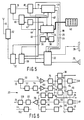
- the cellular telephone subscriber set shown in Figure 5 comprises an antenna 10 connected to a duplex filter 12.
- An r.f. front end section 14 of a receiver is connected to the filter 12.
- a local oscillator signal is derived from a first frequency synthesiser 16 and is supplied to the r.f. front end section 14.
- An IF section 18 including a detector is connected to the r.f. section 14.
- a demodulated output of the IF section 18 is supplied by way of a line 19 to a data processor 20 and to an audio processor 22.
- the data processor 20 provides a data output when a signal is to be transmitted and a mute output when data is on the voice channel. These outputs are connected to the audio processor 22 by lines 24, 25 respectively.
- the audio processor 22 provides a alert tone to an loudspeaker 26 and also processes the audio information, for example expanding companded speech, which in the forward direction is supplied to the earpiece of a telephone handset 28.
- speech from a microphone in the handset 28 is supplied to the audio processor 22 in which it is for example companded before modulating a reverse carrier signal generated by a second frequency synthesiser 30.
- the forward and reverse carrier frequencies are a duplex pair having a frequency separation of 45 MHz.
- the channel spacing is 30 kHz for the AMPS system and 25 kHz for TACS.
- the modulated reverse signal is supplied to a power amplifier 32 from where it is supplied to the duplex filter 12 for transmission via the antenna 10.
- the illustrated apparatus includes a microcontroller 34 together with its associated program read only memory (ROM) 36 and random access memory (RAM) 38 which are directly connected to the microcontroller's address and data busses.
- a key pad 40 is connected to the microcontroller 34.
- the microcontroller 34 is clocked at 9.6 MHz generated by an oscillator 42, its output is supplied also to the first frequency synthesiser 16.
- the first frequency synthesiser 16 includes a frequency divider which divides down the 9.6 MHz clock signal to produce a second clock signal at 1.2 MHz which is synchronised with the first clock signal and which is supplied via a line 44 to the data processor 20, the audio processor 22 and the second frequency synthesiser 30.
- a serial I2C control bus 46 operating at 100 kb/sec interconnects the microcontroller 34, the data processor 20, the audio processor 22 and the first and second frequency synthesisers 16 and 30.
- a two-way synchronous data link 48 is provided between the data processor 20 and the microcontroller 34.
- the data processor 20 and the microcontroller 34 are fabricated in accordance with CMOS technology. It is a feature of CMOS devices that their current consumption is linearly related to the clock frequency of the device.
- the data processor 20 handles the mundane tasks associated with the data present in the forward and reverse signals,. which tasks can be carried out effectively at the second clock frequency of 1.2 MHz by the data processor being hard wired and not operating in software.
- the microcontroller 34 operating at the first clock frequency of 9.6 MHz only has to carry out those tasks which are best suited to processing in software, for example recognising if the address contained in a forward signal is that of the apparatus, and when it is not actually processing data then it can revert to a rest mode in which its current consumption is minimal.
- the IF section 18 comprises an NE 605
- the audio processor 22 comprises integrated circuits NE 5750 and NE 5751
- the data processor 20 will be available as an integrated circuit UMA 1000
- the microcontroller 34 comprises an integrated circuit 80C552
- the frequency synthesisers will be available as integrated circuit UMA 1010.
- the data processor 20 is shown in block schematic form in Figure 6 and comprises mixed analogue and digital circuitry.
- Demodulated analogue data from the IF section 18 ( Figures 5) is supplied on the line 19 to an anti-alias filter 50.
- the filter 50 comprises a continuous time distributed RC active low pass filter and is provided to reduce the possibility of any unwanted signals or high frequency noise present on the line 19 from being aliased into the pass band of a supervisory audio tone (SAT) filter 52 which is connected to the filter 50.
- SAT filter 52 is a switched capacitor filter which provides bandpass filtering of the SAT signals on the line 19 in order to improve the signal to noise ratio prior to the SAT signal recovery and transponding.
- the analogue SAT signal from the filter 52 is applied to an interpolator 54 which functions to increase the sampling rate at the output of the switched capacitor filter 52.
- a strobed comparator 60 provides an analogue to digital interface for the SAT signal.
- the comparator 60 acts as a limiting amplifier which converts the filtered, sampled analogue signals into two state sampled digital signals containing only the zero crossing information from the analogue signal.
- the digital signals are applied to a SAT recovery block 62 in which recovery is performed using a digital phase locked loop.
- the recovered SAT signal is applied to a SAT detector circuit 64 and to a SAT regenerator circuit 66.
- the detector circuit 64 determines which SAT tone is being transmitted and communicates this information via I2C interface 72 operating at 100 kb/s.
- the SAT regeneration circuit 66 generates a digital SAT stream from the recovered SAT stream for transponding back to the base station.
- the regenerated SAT signal is applied to a gated digital-to-analogue (D to A) converter 68 and the analogue SAT signal is combined with other signals in an analogue summer 70.
- D to A digital-to-analogue
- Another strobed comparator 74 is connected to the anti-alias filter 50.
- the comparator 74 is similar to the comparator 60 and provides two-state sampled digital signals containing only the zero-crossing information from the analogue signal.
- a data recovery circuit 76 receives wideband Manchester encoded data in sampled and sliced form and performs the functions of clock recovery, Manchester decoding and data regeneration.
- a dotting detector 78 is connected to the circuit 76 and is used to indicate that a data burst is expected. The dotting detector 78 activates the audio mute line 25 ( Figure 5) to mute the audio processor.
- a word synchronisation detector 80 is also connected to the data recovery circuit 76 and performs the following functions: frame synchronisation, reverse control channel status and valid serving system determination. The functions are associated solely with the forward control channel. Information detailing the status of the reverse control channel is given by the busy/idle bits, see Figure 1. The status of the channel is determined by a majority decision on the last three consecutive Busy/Idle bits.
- a majority voting circuit 82 is also connected to the data recovery circuit 76.
- the circuit 82 performs the functions of (1) identifying the position and validity of frames in the received data stream, (2) extracting 5 repeats of each word from a valid frame and (3) performing a bitwise 3-out-of-5 majority decision on the five repeats of the data word.
- the cleaned data word is applied to an error correction circuit 84.
- This circuit performs a number of functions including (1) extraction of a valid message from the cleaned word, (2) correction of up to one error in a word and (3) communication of received data to the microcontroller 34 (Figure 5) which comprises several lines as shown in Figure 6.
- An arbitration logic circuit 86 is connected to the word synchronisation detector 80.
- the circuit 86 is responsive to the detection of the busy/idle bits to prevent two subscriber sets from transmitting on the same channel.
- the arbitration is specified in the AMPS and TACS specifications and accordingly will not be elaborated upon in the present specification.
- a transmit buffer 88 is provided and has inputs connected to the synchronous data link 48 for receiving data and clock signals.
- the buffer 88 which has an output to the arbitration logic circuit 86, holds data to be transmitted on the RECC or RVC.
- the data from the buffer 88 is applied to the BCH and Manchester encoding circuit 90.
- This circuit 90 performs the following functions: reception of data from the microcontroller, parity generation, message construction and Manchester generation.
- the message construction comprises forming the RECC and RVC data streams from the information it receives from the microcontroller.
- the streams are formed out of four possible field types: dotting, 11 bit synchronisation word, digital colour code and 48 bit code word.
- the encoded digital data stream is applied to another gated D to A converter 92 whose output is connected to the analogue summer 70.
- a signal tone generator (10 kHz for AMPS and 8 kHz for TACS) which provides a signalling tone stream is applied to a further gated D to A converter 96 whose output is also connected to the analogue summer 70.
- the analogue summer 70 combines the three sampled digital signals comprising SAT, the encoded digital data and the signal tone to form a composite signal.
- This composite signal is filtered in an output switched capacitor filter 98 which performs band-limiting of the data processor in accordance with the AMPS or TACS specification.
- the signal from the output filter is applied to a non-critical continuous time distributed RC active low pass clock filter 100 which is used to remove any high frequency components from the output signal.
- the filtered signal is supplied by the line 24 to the audio processor 22 ( Figure 5).
- the data processor 20 further includes a clock generator 102 to provide internal clock frequencies which are derived from the 1.2 MHz clock signal supplied by the line 44.
Landscapes
- Engineering & Computer Science (AREA)
- Computer Networks & Wireless Communication (AREA)
- Signal Processing (AREA)
- Mobile Radio Communication Systems (AREA)
- Advance Control (AREA)
Abstract
Description
- The present invention relates to a cellular telephone apparatus, particularly to a portable subscriber set suitable for use in the Advanced Mobile Phone Service (AMPS) and/or the Total Access Communication System (TACS) which is based on AMPS.
- AMPS is disclosed in detail in the Bell System Technical Journal, January 1979 Vol 58, No. 1 and in the interest of brevity only those aspects pertinent to the present invention will be discussed. In order to facilitate an understanding of the present invention a brief description will be given of some of the data communications in the "forward" direction, that is from a base station at a cell site to a subscriber set, and in the "reverse" direction, that is from a subscriber set to a base station.
- Each cell in a mobile service area is assigned a batch of duplex channels which is different from the batches allocated to neighbouring cells. The two channels of each duplex pair are separated from each other by 45 MHz. However as the overall number of channels is limited then batches of duplex channels are reused in cells geographically separated from each other so that the risk of signals transmitted by one cell site being mistaken by subscriber sets operating in another distant cell which is allocated the same batch of channels is slight. In order to reduce this risk further a system of supervisory audio tones (SATs) is used which are transmitted by base stations and transponded by the subscriber sets.
- Within each cell, one channel of the batch of channels is reserved for setting-up voice channels between subscriber sets and the cell site in which they are currently present. This channel is termed the set-up or access channel and forward and reverse signalling on this channel is exclusively data. Once a voice channel has been set-up data is also transmitted by a "blank and burst" technique in which the voice signal is blanked and data is sent rapidly in a burst. Details of all the possible message formats on the control and voice channels can be derived from for example Bell Systems Technical Journal, January 1979 and the Cellular Mobile Telephone Equipment Specification, July 1982 issued by Advanced Mobile Phone Service Inc. However, four of the more pertinant message formats will be described with reference to Figures 1 to 4 of the accompanying drawings.
- Figure 1 shows the forward control channel (FOCC) message stream which consists of three discrete information streams called stream A, stream B and busy/idle stream denoted by the arrows. Each mobile apparatus monitors stream A or stream B and the busy/idle stream.
- The message begins with a 10-bit dotting sequence (1010101010) D for bit synchronisation, and is followed by an 11-bit word synchronisation sequence (11100010010) WS to achieve synchronisation with the incoming data. Each word is encoded and contains 40 bits, including parity and is repeated five times. The coding is a linear systematic block code, particularly a (48, 28) BCH code.
- For ease of reference the five transmissions of the words A and B have be referenced A1 to A5 and B1 to B5.
- Figure 2 shows the forward voice channel (FVC) data stream, its data rate being 10 kb/sec for AMPS and 8 kb/sec for TACS. The datastream commences with a 101-bit dotting sequence (D101) followed by an 11-bit word synchronisation sequence and the first repeat of the word W1. Each word encoded into a (40,28) BCH linear systematic block code is repeated ten more times, referenced W2 to W11; each repeat being preceded by a 37-bit dotting sequence and the 11-bit word synchronising sequence.
- Figure 3 illustrates the data stream on the reverse control channel (RECC). The data stream is discontinuous and the data rate is 10 kb/sec for AMPS and 8 kb/sec for TACS. The RECC data stream comprises 30 bits of dotting sequence, D, an 11-bit word synchronisation sequence, WS, and a 7-bit coded digital colour code CDCC (see the Cellular Mobile Telephone equipment Specification referred to above for further information) followed by a 48 bit first word repeated five times (5xRW1), a 48 bit second word repeated five times (5xRW2), a 48 bit third word repeated five times (5xRW3) and so on. The dotting sequence, D, the word synchronisation sequence WS and the CDCC constitute a seizure precursor SP. The 48 bit words are encoded in accordance with a BCH (48,36) linear systematic block code.
- Finally Figure 4 shows the reverse voice channel (RVC) data stream which from time to time interrupts analogue voice signals. The data stream commences with a 101 bit dotting sequence D(101) followed by an 11-bit word synchronisation sequence and the first repeat of a first 48 bit word 1RW1. Thereafter there are four more repeats of the first word, denoted by 2RW1 to 5RW1, each repeat being preceded by a 37 bit dotting sequence and an 11 bit word synchronisation sequence. This data stream is followed by 37 bits of dotting sequence and 11 bits of word synchronisation sequence with five repeats of a second word 1RW2 to 5RW2, and so on.
- In a subscriber set, which term includes portable and mobile subscriber sets, it has been customary to process digitally all the data and control information received or to be transmitted as well as provide the internal control information for the subscriber set by means of a logic unit constituted by a microprocessor. In order to be able to implement the required functions in software requires many programme steps which in turn means a high clock frequency and a high current consumption. However other sections of the subscriber sets operate at other clock frequencies and in consequence it is necessary to provide several clock generators formed by separate oscillators in each set. A drawback to having several oscillators is that they are expensive, current hungry and are sources of spurious signals.
- An object of the present invention is to provide an architecture for a cellular telephone apparatus which mitigates these drawbacks.
- According to the present invention there is provided a cellular telephone apparatus comprising a duplex transceiver, a logic unit formed by a data processor and a microcontroller, the data processor being coupled to the transceiver for processing data received by or to be transmitted by the transceiver and the microcontroller being coupled to the data processor for utilising data produced by the data processor in response to a received data stream and for providing data for transmission, a clock generator for supplying a first clock signal to the microcontroller and means for deriving from the first clock signal a second clock signal which is supplied to the data processor, the second clock signal being of lower frequency than and in synchronism with, the first clock signal to the data processor.
- The present invention is based on a recognition of the fact that many of the functions previously carried out in software in the logic unit could be carried out in an architecture comprising a hard-wired data processor and a micro-controller, the data processor operating at a lower clock frequency than the micro-controller which in turn is energised only when (1) decoded data sent in the forward direction is ready to be processed, (2) data is being assembled for encoding in the data processor and (3) control signals are necessary for the operation of the mobile apparatus. Furthermore by deriving the second clock frequency from the first clock frequency then a second clock generator is not required saving expense, current and chip area. Also by having synchronised first and second clock signals there will be fewer spurious signals than when separate unsynchronised clock generators are used.
- In an embodiment of the apparatus made in accordance with the present invention an oscillator is provided which generates the first clock signal, say 9.6 MHz. The first clock signal is also supplied to a frequency synthesiser for providing a local oscillator signal to the transceiver. The frequency synthesiser includes a divider which produces the second clock signal, say 1.2 MHz, by dividing down the first clock signal. The second clock signal is supplied not only to the data processor but also to an audio processing circuit as well as to another frequency synthesiser for producing the master oscillator frequency of the transmitting section of the transceiver. Dividing down the first clock signal at the frequency synthesiser and distributing the divided down signal as the second clock signal to the dataprocessor and other circuit elements which require this signal also has advantages over the possibility of distributing the first clock signal to all the circuit elements requiring a clock signal and providing a frequency divider in each of those circuit elements which require a lower clock frequency. These advantages are current saving because frequency dividing is a relatively high current consuming process and also a relatively high power would be required to drive the first clock signal to each of the required circuit elements. Another advantage is that the emission of spurious signals is less of a problem at lower frequencies. A further advantage of dividing down the frequency of the first clock signal is that both the first and second clock signals are in synchronism further reducing the possibility of spurious signals.
- By hiving off the control functions to the data processor, a control bus within the subscriber set may comprise a serial I²C bus comprising one data line and one clock line. The clock line is operated at a sub-division of the second clock signal which also enables some of the above mentioned advantages to be realised. Additionally a serial I²C bus occupies less board area than a parallel control bus, because there are fewer tracks. Also an integrated circuit to which the I²C bus is connected only requires two pins for the control bus connection thus saving on the number of pins which would otherwise have to be provided in order to effect a connection when using a parallel control bus.
- The present invention will now be described, by way of example, with reference to the accompanying drawings, wherein:
- Figure 1 illustrates the data format for the forward control channel (FOCC) message stream,
- Figure 2 illustrates the data format for the forward voice channel (FVC),
- Figure 3 illustrates the data format for the reverse control channel (RECC),
- Figure 4 illustrates the data format for the reverse voice channel (RVC),
- Figure 5 is a simplified block schematic diagram of a cellular telephone subscriber set made in accordance with the present invention, and
- Figure 6 is a block schematic diagram of a data processor used in the apparatus shown in Figure 1.
- In the drawings the same reference numerals have been used to indicate corresponding features.
- Figures 1 to 4 have been described in the preamble.
- The cellular telephone subscriber set shown in Figure 5 comprises an
antenna 10 connected to aduplex filter 12. An r.f.front end section 14 of a receiver is connected to thefilter 12. A local oscillator signal is derived from afirst frequency synthesiser 16 and is supplied to the r.f.front end section 14. An IFsection 18 including a detector is connected to the r.f.section 14. A demodulated output of theIF section 18 is supplied by way of aline 19 to adata processor 20 and to anaudio processor 22. Thedata processor 20 provides a data output when a signal is to be transmitted and a mute output when data is on the voice channel. These outputs are connected to theaudio processor 22 bylines audio processor 22 provides a alert tone to anloudspeaker 26 and also processes the audio information, for example expanding companded speech, which in the forward direction is supplied to the earpiece of atelephone handset 28. In the reverse direction speech from a microphone in thehandset 28 is supplied to theaudio processor 22 in which it is for example companded before modulating a reverse carrier signal generated by asecond frequency synthesiser 30. The forward and reverse carrier frequencies are a duplex pair having a frequency separation of 45 MHz. The channel spacing is 30 kHz for the AMPS system and 25 kHz for TACS. The modulated reverse signal is supplied to apower amplifier 32 from where it is supplied to theduplex filter 12 for transmission via theantenna 10. - The illustrated apparatus includes a
microcontroller 34 together with its associated program read only memory (ROM) 36 and random access memory (RAM) 38 which are directly connected to the microcontroller's address and data busses. Akey pad 40 is connected to themicrocontroller 34. Themicrocontroller 34 is clocked at 9.6 MHz generated by anoscillator 42, its output is supplied also to thefirst frequency synthesiser 16. Thefirst frequency synthesiser 16 includes a frequency divider which divides down the 9.6 MHz clock signal to produce a second clock signal at 1.2 MHz which is synchronised with the first clock signal and which is supplied via aline 44 to thedata processor 20, theaudio processor 22 and thesecond frequency synthesiser 30. - A serial
I²C control bus 46 operating at 100 kb/sec interconnects themicrocontroller 34, thedata processor 20, theaudio processor 22 and the first andsecond frequency synthesisers - A two-way synchronous data link 48 is provided between the
data processor 20 and themicrocontroller 34. - The
data processor 20 and themicrocontroller 34 are fabricated in accordance with CMOS technology. It is a feature of CMOS devices that their current consumption is linearly related to the clock frequency of the device. In the apparatus made in accordance with the present invention thedata processor 20 handles the mundane tasks associated with the data present in the forward and reverse signals,. which tasks can be carried out effectively at the second clock frequency of 1.2 MHz by the data processor being hard wired and not operating in software. Themicrocontroller 34 operating at the first clock frequency of 9.6 MHz only has to carry out those tasks which are best suited to processing in software, for example recognising if the address contained in a forward signal is that of the apparatus, and when it is not actually processing data then it can revert to a rest mode in which its current consumption is minimal. - In implementing the subscriber set the
IF section 18 comprises an NE 605, theaudio processor 22 comprises integrated circuits NE 5750 and NE 5751, thedata processor 20 will be available as an integrated circuit UMA 1000, themicrocontroller 34 comprises an integrated circuit 80C552 and the frequency synthesisers will be available as integrated circuit UMA 1010. - The
data processor 20 is shown in block schematic form in Figure 6 and comprises mixed analogue and digital circuitry. Demodulated analogue data from the IF section 18 (Figures 5) is supplied on theline 19 to ananti-alias filter 50. Thefilter 50 comprises a continuous time distributed RC active low pass filter and is provided to reduce the possibility of any unwanted signals or high frequency noise present on theline 19 from being aliased into the pass band of a supervisory audio tone (SAT) filter 52 which is connected to thefilter 50. TheSAT filter 52 is a switched capacitor filter which provides bandpass filtering of the SAT signals on theline 19 in order to improve the signal to noise ratio prior to the SAT signal recovery and transponding. The analogue SAT signal from thefilter 52 is applied to aninterpolator 54 which functions to increase the sampling rate at the output of the switchedcapacitor filter 52. A strobedcomparator 60 provides an analogue to digital interface for the SAT signal. Thecomparator 60 acts as a limiting amplifier which converts the filtered, sampled analogue signals into two state sampled digital signals containing only the zero crossing information from the analogue signal. The digital signals are applied to aSAT recovery block 62 in which recovery is performed using a digital phase locked loop. The recovered SAT signal is applied to aSAT detector circuit 64 and to aSAT regenerator circuit 66. Thedetector circuit 64 determines which SAT tone is being transmitted and communicates this information viaI²C interface 72 operating at 100 kb/s. - The
SAT regeneration circuit 66 generates a digital SAT stream from the recovered SAT stream for transponding back to the base station. The regenerated SAT signal is applied to a gated digital-to-analogue (D to A)converter 68 and the analogue SAT signal is combined with other signals in ananalogue summer 70. - Another strobed
comparator 74 is connected to theanti-alias filter 50. Thecomparator 74 is similar to thecomparator 60 and provides two-state sampled digital signals containing only the zero-crossing information from the analogue signal. Adata recovery circuit 76 receives wideband Manchester encoded data in sampled and sliced form and performs the functions of clock recovery, Manchester decoding and data regeneration. A dottingdetector 78 is connected to thecircuit 76 and is used to indicate that a data burst is expected. The dottingdetector 78 activates the audio mute line 25 (Figure 5) to mute the audio processor. - A
word synchronisation detector 80 is also connected to thedata recovery circuit 76 and performs the following functions: frame synchronisation, reverse control channel status and valid serving system determination. The functions are associated solely with the forward control channel. Information detailing the status of the reverse control channel is given by the busy/idle bits, see Figure 1. The status of the channel is determined by a majority decision on the last three consecutive Busy/Idle bits. - A
majority voting circuit 82 is also connected to thedata recovery circuit 76. Thecircuit 82 performs the functions of (1) identifying the position and validity of frames in the received data stream, (2) extracting 5 repeats of each word from a valid frame and (3) performing a bitwise 3-out-of-5 majority decision on the five repeats of the data word. - The cleaned data word is applied to an
error correction circuit 84. This circuit performs a number of functions including (1) extraction of a valid message from the cleaned word, (2) correction of up to one error in a word and (3) communication of received data to the microcontroller 34 (Figure 5) which comprises several lines as shown in Figure 6. - An
arbitration logic circuit 86 is connected to theword synchronisation detector 80. Thecircuit 86 is responsive to the detection of the busy/idle bits to prevent two subscriber sets from transmitting on the same channel. The arbitration is specified in the AMPS and TACS specifications and accordingly will not be elaborated upon in the present specification. - A transmit
buffer 88 is provided and has inputs connected to the synchronous data link 48 for receiving data and clock signals. Thebuffer 88 which has an output to thearbitration logic circuit 86, holds data to be transmitted on the RECC or RVC. The data from thebuffer 88 is applied to the BCH andManchester encoding circuit 90. Thiscircuit 90 performs the following functions: reception of data from the microcontroller, parity generation, message construction and Manchester generation. The message construction comprises forming the RECC and RVC data streams from the information it receives from the microcontroller. The streams are formed out of four possible field types: dotting, 11 bit synchronisation word, digital colour code and 48 bit code word. The encoded digital data stream is applied to another gated D to Aconverter 92 whose output is connected to theanalogue summer 70. - A signal tone generator (10 kHz for AMPS and 8 kHz for TACS) which provides a signalling tone stream is applied to a further gated D to A
converter 96 whose output is also connected to theanalogue summer 70. - The
analogue summer 70 combines the three sampled digital signals comprising SAT, the encoded digital data and the signal tone to form a composite signal. This composite signal is filtered in an output switchedcapacitor filter 98 which performs band-limiting of the data processor in accordance with the AMPS or TACS specification. The signal from the output filter is applied to a non-critical continuous time distributed RC active lowpass clock filter 100 which is used to remove any high frequency components from the output signal. The filtered signal is supplied by theline 24 to the audio processor 22 (Figure 5). - The
data processor 20 further includes aclock generator 102 to provide internal clock frequencies which are derived from the 1.2 MHz clock signal supplied by theline 44. - Various other configurations of data processors are possible without departing from the scope of the invention as defined in the appended claims.
Claims (13)
Applications Claiming Priority (2)
| Application Number | Priority Date | Filing Date | Title |
|---|---|---|---|
| GB8725626A GB2212030A (en) | 1987-11-02 | 1987-11-02 | Cellular telephone apparatus |
| GB8725626 | 1987-11-02 |
Publications (2)
| Publication Number | Publication Date |
|---|---|
| EP0315260A2 true EP0315260A2 (en) | 1989-05-10 |
| EP0315260A3 EP0315260A3 (en) | 1990-07-25 |
Family
ID=10626289
Family Applications (1)
| Application Number | Title | Priority Date | Filing Date |
|---|---|---|---|
| EP88202406A Withdrawn EP0315260A3 (en) | 1987-11-02 | 1988-10-28 | Cellular telephone apparatus |
Country Status (7)
| Country | Link |
|---|---|
| US (1) | US4965820A (en) |
| EP (1) | EP0315260A3 (en) |
| JP (1) | JPH01151326A (en) |
| KR (1) | KR890009137A (en) |
| DK (1) | DK603488A (en) |
| FI (1) | FI884980A (en) |
| GB (1) | GB2212030A (en) |
Cited By (10)
| Publication number | Priority date | Publication date | Assignee | Title |
|---|---|---|---|---|
| EP0343528A2 (en) * | 1988-05-21 | 1989-11-29 | Fujitsu Limited | Mobile telephone terminal |
| EP0447302A1 (en) * | 1990-03-16 | 1991-09-18 | Matra Communication | Time-multiplexed radio communication device |
| EP0475776A2 (en) * | 1990-09-13 | 1992-03-18 | Pitney Bowes, Inc. | Apparatus for resetting a postage meter |
| EP0553862A2 (en) * | 1992-01-31 | 1993-08-04 | Canon Kabushiki Kaisha | Portable electronic device having a radio transmit-receive unit and a computer unit |
| EP0590607A1 (en) * | 1992-09-29 | 1994-04-06 | Oki Electric Industry Co., Ltd. | Low-power baud rate generator |
| WO1994013089A1 (en) * | 1992-11-27 | 1994-06-09 | Nokia Telecommunications Oy | Radio system |
| FR2699027A1 (en) * | 1992-12-04 | 1994-06-10 | Info Telecom | Method for processing information within a receiver, in particular paging, and corresponding receiver. |
| FR2701182A1 (en) * | 1993-01-29 | 1994-08-05 | Murata Machinery Ltd | Portable telephone |
| WO1996011556A1 (en) * | 1994-10-06 | 1996-04-18 | Qualcomm Incorporated | Method for power saving in a cellular radiotelephone apparatus |
| FR2766319A1 (en) * | 1997-07-15 | 1999-01-22 | Alsthom Cge Alcatel | ELECTRONIC DEVICE, IN PARTICULAR RADIOCOMMUNICATION DEVICE, OF THE TYPE LIKELY TO SWITCH BETWEEN AT LEAST TWO MODES OF OPERATION |
Families Citing this family (10)
| Publication number | Priority date | Publication date | Assignee | Title |
|---|---|---|---|---|
| US5987639A (en) * | 1992-01-21 | 1999-11-16 | Nokia Mobile Phones Ltd. | Data decoding logic in a mobile phone |
| US6144859A (en) * | 1993-08-27 | 2000-11-07 | Aeris Communications, Inc. | Wireless cellular communicator system and apparatus |
| US5555287A (en) * | 1992-07-21 | 1996-09-10 | Advanced Micro Devices, Inc. | Integrated circuit and cordless telephone using the integrated circuit |
| US5337345A (en) * | 1992-07-29 | 1994-08-09 | Novatel Communications | System for securing mobile telephones from unauthorized transmission |
| US5594740A (en) | 1993-08-27 | 1997-01-14 | Axion Logistics Corporation | Wireless communications application specific enabling method and apparatus |
| US5999808A (en) * | 1995-12-12 | 1999-12-07 | Aeris Communications, Inc. | Wireless gaming method |
| US5845203A (en) * | 1996-01-25 | 1998-12-01 | Aertis Cormmunications | Remote access application messaging wireless method |
| TW328195B (en) * | 1996-07-04 | 1998-03-11 | Seiko Denshi Kk | The semiconductor IC for communication and its electricity-economized method |
| DE19733530C2 (en) * | 1997-08-02 | 2003-10-09 | Philips Intellectual Property | mobile device |
| US9191912B2 (en) * | 2013-09-26 | 2015-11-17 | Adc Telecommunications, Inc. | Systems and methods for location determination |
Citations (1)
| Publication number | Priority date | Publication date | Assignee | Title |
|---|---|---|---|---|
| JPS59200537A (en) * | 1983-04-27 | 1984-11-13 | Nippon Telegr & Teleph Corp <Ntt> | Mobile communication equipment |
Family Cites Families (5)
| Publication number | Priority date | Publication date | Assignee | Title |
|---|---|---|---|---|
| US4486624A (en) * | 1980-09-15 | 1984-12-04 | Motorola, Inc. | Microprocessor controlled radiotelephone transceiver |
| US4618997A (en) * | 1984-03-23 | 1986-10-21 | General Research Of Electronics, Inc. | Portable transceiver |
| US4637022A (en) * | 1984-12-21 | 1987-01-13 | Motorola, Inc. | Internally register-modelled, serially-bussed radio system |
| US4829554A (en) * | 1985-01-31 | 1989-05-09 | Harris Corporation | Cellular mobile telephone system and method |
| US4718080A (en) * | 1985-12-16 | 1988-01-05 | Serrano Arthur L | Microprocessor controlled interface for cellular system |
-
1987
- 1987-11-02 GB GB8725626A patent/GB2212030A/en not_active Withdrawn
-
1988
- 1988-10-28 FI FI884980A patent/FI884980A/en not_active IP Right Cessation
- 1988-10-28 DK DK603488A patent/DK603488A/en not_active Application Discontinuation
- 1988-10-28 EP EP88202406A patent/EP0315260A3/en not_active Withdrawn
- 1988-10-31 KR KR1019880014201A patent/KR890009137A/en not_active Application Discontinuation
- 1988-10-31 JP JP63273366A patent/JPH01151326A/en active Pending
- 1988-11-01 US US07/265,648 patent/US4965820A/en not_active Expired - Fee Related
Patent Citations (1)
| Publication number | Priority date | Publication date | Assignee | Title |
|---|---|---|---|---|
| JPS59200537A (en) * | 1983-04-27 | 1984-11-13 | Nippon Telegr & Teleph Corp <Ntt> | Mobile communication equipment |
Non-Patent Citations (5)
| Title |
|---|
| NEC RESEARCH & DEVELOPMENT, no. 87, October 1987, pages 34-43, Tokyo, JP; Y. TAMURA et al.: "Hand-held portable equipment for cellular mobile telephone" * |
| PATENT ABSTRACTS OF JAPAN, vol. 9, no. 61 (E-303)[1784] 19th March 1985; & JP-A-59 200 537 (NIPPON DENSHIN DENWA KOSHA) 13-11-1984 * |
| PROCEEDINGS OF THE 30TH ANNUAL CONFERENCE OF THE I.E.E.E. VEHICULAR TECHNOLOGY SOCIETY, Dearborn, Michigan, 15th-17th September 1980, pages 1-7, Bohn Printing Co., Utica, Michigan, US; A.J. LEITICH et al.: "Portable telephones for cellular systems" * |
| PROCEEDINGS OF THE INTERNATIONAL CONGRESS ON TRANSPORTATION ELECTRONICS, 1986, pages 99-106, Society of Automotive Engineers, Inc., Warrendale, PA, US; K. KAWATA et al.: "Digital LSI: The key to refining the automotive audio system" * |
| TELCOM REPORT vol. 9, Sonderheft: "Nachrichten}bertragung auf Funkwegen, pages 313-318, M}nchen, DE; F. BECKER et al.: "Die Mobilstation im Spannungsfeld von Innovation, Rationalisierung und technischen Anforderungen" * |
Cited By (23)
| Publication number | Priority date | Publication date | Assignee | Title |
|---|---|---|---|---|
| EP0343528A2 (en) * | 1988-05-21 | 1989-11-29 | Fujitsu Limited | Mobile telephone terminal |
| EP0343528A3 (en) * | 1988-05-21 | 1992-03-04 | Fujitsu Limited | Mobile telephone terminal |
| EP0447302A1 (en) * | 1990-03-16 | 1991-09-18 | Matra Communication | Time-multiplexed radio communication device |
| FR2659812A1 (en) * | 1990-03-16 | 1991-09-20 | Matra Communication | TIME MULTIPLEXING RADIO COMMUNICATION DEVICE. |
| US5202914A (en) * | 1990-09-13 | 1993-04-13 | Pitney Bowes Inc. | System for resetting a postage meter |
| EP0475776A3 (en) * | 1990-09-13 | 1992-06-10 | Pitney Bowes, Inc. | Apparatus for resetting a postage meter |
| EP0475776A2 (en) * | 1990-09-13 | 1992-03-18 | Pitney Bowes, Inc. | Apparatus for resetting a postage meter |
| EP0553862A2 (en) * | 1992-01-31 | 1993-08-04 | Canon Kabushiki Kaisha | Portable electronic device having a radio transmit-receive unit and a computer unit |
| US5604928A (en) * | 1992-01-31 | 1997-02-18 | Canon Kabushiki Kaisha | Portable electronic device with radio communication and controlled computer status |
| EP0553862A3 (en) * | 1992-01-31 | 1994-11-17 | Canon Kk | Portable electronic device having a radio transmit-receive unit and a computer unit |
| US5398007A (en) * | 1992-09-29 | 1995-03-14 | Oki Electric Industry Co., Ltd. | Low-power baud rate generator including two oscillators |
| EP0590607A1 (en) * | 1992-09-29 | 1994-04-06 | Oki Electric Industry Co., Ltd. | Low-power baud rate generator |
| WO1994013089A1 (en) * | 1992-11-27 | 1994-06-09 | Nokia Telecommunications Oy | Radio system |
| US5678192A (en) * | 1992-11-27 | 1997-10-14 | Nokia Telecommunications Oy | Radio system |
| FR2699027A1 (en) * | 1992-12-04 | 1994-06-10 | Info Telecom | Method for processing information within a receiver, in particular paging, and corresponding receiver. |
| WO1994014290A1 (en) * | 1992-12-04 | 1994-06-23 | Info Telecom | Method for processing information within a receiver, particularly a paging receiver, and receiver therefor |
| FR2701182A1 (en) * | 1993-01-29 | 1994-08-05 | Murata Machinery Ltd | Portable telephone |
| WO1996011556A1 (en) * | 1994-10-06 | 1996-04-18 | Qualcomm Incorporated | Method for power saving in a cellular radiotelephone apparatus |
| US5566357A (en) * | 1994-10-06 | 1996-10-15 | Qualcomm Incorporated | Power reduction in a cellular radiotelephone |
| AU688985B2 (en) * | 1994-10-06 | 1998-03-19 | Qualcomm Incorporated | Method for power saving in a cellular radiotelephone apparatus |
| CN1082326C (en) * | 1994-10-06 | 2002-04-03 | 夸尔柯姆股份有限公司 | Power saving in celluar dadiotelephone apparatus |
| FR2766319A1 (en) * | 1997-07-15 | 1999-01-22 | Alsthom Cge Alcatel | ELECTRONIC DEVICE, IN PARTICULAR RADIOCOMMUNICATION DEVICE, OF THE TYPE LIKELY TO SWITCH BETWEEN AT LEAST TWO MODES OF OPERATION |
| EP0895434A1 (en) * | 1997-07-15 | 1999-02-03 | Alcatel | Electronic device, especially a radiocommunication device, of the type that can switch between at least two different function modes |
Also Published As
| Publication number | Publication date |
|---|---|
| GB2212030A (en) | 1989-07-12 |
| JPH01151326A (en) | 1989-06-14 |
| KR890009137A (en) | 1989-07-15 |
| FI884980A0 (en) | 1988-10-28 |
| EP0315260A3 (en) | 1990-07-25 |
| US4965820A (en) | 1990-10-23 |
| GB8725626D0 (en) | 1987-12-09 |
| DK603488D0 (en) | 1988-10-28 |
| FI884980A (en) | 1989-05-03 |
| DK603488A (en) | 1989-05-03 |
Similar Documents
| Publication | Publication Date | Title |
|---|---|---|
| US4965820A (en) | Cellular telephone apparatus | |
| US5396653A (en) | Cellular telephone signalling circuit operable with different cellular telephone systems | |
| EP0937349B1 (en) | Synchronization in tdma systems in a non-real-time fashion | |
| KR100297011B1 (en) | Wireless Telephone System for Long Range Subscribers | |
| JP2766430B2 (en) | Method and apparatus for delivering wireless telephone signals over a cable television network | |
| JP3222904B2 (en) | Signal processing circuit for European cellular digital radio telephone system | |
| CN1048472A (en) | The method of keeping mobile communication of mobile assist type | |
| WO1993002531A1 (en) | Prioritized data transfer method and apparatus for a radiotelephone peripheral | |
| US5038342A (en) | TDM/FDM communication system supporting both TDM and FDM-only communication units | |
| US6044486A (en) | Method and device for majority vote optimization over wireless communication channels | |
| US6304761B1 (en) | Mobile unit communication apparatus having digital and analog communication modes and a method of controlling the same | |
| CN1328919C (en) | Synchronization of multi-mode base station using common system clock | |
| US5426642A (en) | Satellite broadcast communication system | |
| US5697062A (en) | Method and apparatus for improved link establishment and monitoring in a communications system | |
| US20030153327A1 (en) | Cellular communication apparatus and channel capture method | |
| JP3950668B2 (en) | Digital radio system | |
| US5502437A (en) | Receiver isolation scheme | |
| JPH02256341A (en) | Synchronizing recovery circuit recovering word synchronization and radio communication equipment using the circuit | |
| JPS58161427A (en) | Radio equipment | |
| KR100193813B1 (en) | Apparatus and method for sending paging data | |
| JPS63136835A (en) | Simultaneous transmission and reception equipment | |
| JPH09181647A (en) | Transmitter-receiver and transmission and reception system | |
| WO1998039864A1 (en) | Digital signal receiver | |
| JP3426856B2 (en) | Communication device | |
| JPH0314854Y2 (en) |
Legal Events
| Date | Code | Title | Description |
|---|---|---|---|
| PUAI | Public reference made under article 153(3) epc to a published international application that has entered the european phase |
Free format text: ORIGINAL CODE: 0009012 |
|
| AK | Designated contracting states |
Kind code of ref document: A2 Designated state(s): DE FR GB IT SE |
|
| PUAL | Search report despatched |
Free format text: ORIGINAL CODE: 0009013 |
|
| AK | Designated contracting states |
Kind code of ref document: A3 Designated state(s): DE FR GB IT SE |
|
| 17P | Request for examination filed |
Effective date: 19901219 |
|
| 17Q | First examination report despatched |
Effective date: 19930716 |
|
| STAA | Information on the status of an ep patent application or granted ep patent |
Free format text: STATUS: THE APPLICATION IS DEEMED TO BE WITHDRAWN |
|
| 18D | Application deemed to be withdrawn |
Effective date: 19940618 |