EP0314465A2 - A semiconductor device having a vertical power mosfet fabricated in an isolated form on a semiconductor substrate - Google Patents
A semiconductor device having a vertical power mosfet fabricated in an isolated form on a semiconductor substrate Download PDFInfo
- Publication number
- EP0314465A2 EP0314465A2 EP88310089A EP88310089A EP0314465A2 EP 0314465 A2 EP0314465 A2 EP 0314465A2 EP 88310089 A EP88310089 A EP 88310089A EP 88310089 A EP88310089 A EP 88310089A EP 0314465 A2 EP0314465 A2 EP 0314465A2
- Authority
- EP
- European Patent Office
- Prior art keywords
- type
- semiconductor substrate
- diffused region
- region
- semiconductor
- Prior art date
- Legal status (The legal status is an assumption and is not a legal conclusion. Google has not performed a legal analysis and makes no representation as to the accuracy of the status listed.)
- Granted
Links
- 239000004065 semiconductor Substances 0.000 title claims abstract description 54
- 239000000758 substrate Substances 0.000 title claims abstract description 50
- 230000000295 complement effect Effects 0.000 claims description 2
- 239000012535 impurity Substances 0.000 description 27
- 238000009792 diffusion process Methods 0.000 description 20
- 238000002955 isolation Methods 0.000 description 19
- 238000004519 manufacturing process Methods 0.000 description 13
- 230000003071 parasitic effect Effects 0.000 description 10
- 229910021420 polycrystalline silicon Inorganic materials 0.000 description 8
- 229920005591 polysilicon Polymers 0.000 description 8
- 238000009826 distribution Methods 0.000 description 5
- 229910052796 boron Inorganic materials 0.000 description 4
- 230000015556 catabolic process Effects 0.000 description 4
- 230000000694 effects Effects 0.000 description 4
- 239000005360 phosphosilicate glass Substances 0.000 description 4
- ZOXJGFHDIHLPTG-UHFFFAOYSA-N Boron Chemical compound [B] ZOXJGFHDIHLPTG-UHFFFAOYSA-N 0.000 description 3
- 230000015572 biosynthetic process Effects 0.000 description 3
- XEEYBQQBJWHFJM-UHFFFAOYSA-N Iron Chemical compound [Fe] XEEYBQQBJWHFJM-UHFFFAOYSA-N 0.000 description 2
- 238000001514 detection method Methods 0.000 description 2
- 238000010586 diagram Methods 0.000 description 2
- 238000002513 implantation Methods 0.000 description 2
- 239000011261 inert gas Substances 0.000 description 2
- 238000000034 method Methods 0.000 description 2
- XPIJWUTXQAGSLK-UHFFFAOYSA-N ozenoxacin Chemical compound C1=C(C)C(NC)=NC=C1C1=CC=C2C(=O)C(C(O)=O)=CN(C3CC3)C2=C1C XPIJWUTXQAGSLK-UHFFFAOYSA-N 0.000 description 2
- 230000002093 peripheral effect Effects 0.000 description 2
- OAICVXFJPJFONN-UHFFFAOYSA-N Phosphorus Chemical compound [P] OAICVXFJPJFONN-UHFFFAOYSA-N 0.000 description 1
- 229910052787 antimony Inorganic materials 0.000 description 1
- WATWJIUSRGPENY-UHFFFAOYSA-N antimony atom Chemical compound [Sb] WATWJIUSRGPENY-UHFFFAOYSA-N 0.000 description 1
- -1 boron ions Chemical class 0.000 description 1
- 238000005094 computer simulation Methods 0.000 description 1
- 238000005336 cracking Methods 0.000 description 1
- 239000002019 doping agent Substances 0.000 description 1
- 230000005684 electric field Effects 0.000 description 1
- 229910052742 iron Inorganic materials 0.000 description 1
- 231100000989 no adverse effect Toxicity 0.000 description 1
- 229910052698 phosphorus Inorganic materials 0.000 description 1
- 239000011574 phosphorus Substances 0.000 description 1
Images


Classifications
-
- H—ELECTRICITY
- H01—ELECTRIC ELEMENTS
- H01L—SEMICONDUCTOR DEVICES NOT COVERED BY CLASS H10
- H01L27/00—Devices consisting of a plurality of semiconductor or other solid-state components formed in or on a common substrate
- H01L27/02—Devices consisting of a plurality of semiconductor or other solid-state components formed in or on a common substrate including semiconductor components specially adapted for rectifying, oscillating, amplifying or switching and having potential barriers; including integrated passive circuit elements having potential barriers
- H01L27/04—Devices consisting of a plurality of semiconductor or other solid-state components formed in or on a common substrate including semiconductor components specially adapted for rectifying, oscillating, amplifying or switching and having potential barriers; including integrated passive circuit elements having potential barriers the substrate being a semiconductor body
- H01L27/08—Devices consisting of a plurality of semiconductor or other solid-state components formed in or on a common substrate including semiconductor components specially adapted for rectifying, oscillating, amplifying or switching and having potential barriers; including integrated passive circuit elements having potential barriers the substrate being a semiconductor body including only semiconductor components of a single kind
- H01L27/085—Devices consisting of a plurality of semiconductor or other solid-state components formed in or on a common substrate including semiconductor components specially adapted for rectifying, oscillating, amplifying or switching and having potential barriers; including integrated passive circuit elements having potential barriers the substrate being a semiconductor body including only semiconductor components of a single kind including field-effect components only
- H01L27/088—Devices consisting of a plurality of semiconductor or other solid-state components formed in or on a common substrate including semiconductor components specially adapted for rectifying, oscillating, amplifying or switching and having potential barriers; including integrated passive circuit elements having potential barriers the substrate being a semiconductor body including only semiconductor components of a single kind including field-effect components only the components being field-effect transistors with insulated gate
-
- H—ELECTRICITY
- H01—ELECTRIC ELEMENTS
- H01L—SEMICONDUCTOR DEVICES NOT COVERED BY CLASS H10
- H01L21/00—Processes or apparatus adapted for the manufacture or treatment of semiconductor or solid state devices or of parts thereof
- H01L21/70—Manufacture or treatment of devices consisting of a plurality of solid state components formed in or on a common substrate or of parts thereof; Manufacture of integrated circuit devices or of parts thereof
- H01L21/71—Manufacture of specific parts of devices defined in group H01L21/70
- H01L21/76—Making of isolation regions between components
- H01L21/761—PN junctions
-
- H—ELECTRICITY
- H01—ELECTRIC ELEMENTS
- H01L—SEMICONDUCTOR DEVICES NOT COVERED BY CLASS H10
- H01L27/00—Devices consisting of a plurality of semiconductor or other solid-state components formed in or on a common substrate
- H01L27/02—Devices consisting of a plurality of semiconductor or other solid-state components formed in or on a common substrate including semiconductor components specially adapted for rectifying, oscillating, amplifying or switching and having potential barriers; including integrated passive circuit elements having potential barriers
- H01L27/0203—Particular design considerations for integrated circuits
- H01L27/0248—Particular design considerations for integrated circuits for electrical or thermal protection, e.g. electrostatic discharge [ESD] protection
- H01L27/0251—Particular design considerations for integrated circuits for electrical or thermal protection, e.g. electrostatic discharge [ESD] protection for MOS devices
Definitions
- the present invention relates to a semiconductor device and, more particularly, to a semiconductor device having a plurality of circuit elements including a vertical MOSFET isolated from the other circuit elements.
- the vertical MOSFET In the integrated circuit device having a vertical MOSFET as an output transistor and other circuit elements formed on the same chip, the vertical MOSFET must be isolated from the other circuit elements.
- a junction isolation, and a dielectric isolation are examples of the isolation structure in the prior art.
- Fig. 5 shows the junction isolation structure in a prior art (see IEEE 1987 CUSTOM INTEGRATED CIRCUIT CONFERENCE, p. 276), while Fig. 6 shows the dielectric isolation structure in another prior art (see Japanese Patent Laid-Open No. 196576/1986).
- These conventional isolation structures suffer, however, from the disadvantage that the manufacturing process is complicated and the production cost is high.
- junction isolation structure shown in Fig. 5 after an N+ buried layer 51 is provided in an N+-substrate 1, a P-type epitaxial layer 52 and an N-type epitaxial layer 3 are stacked thereon successively. Then, a P-type impurity is diffused into the N-type epitaxial layer 3 from the surface to form a P-type diffused layer 53 for isolation.
- this structure requires a complicated process.
- vertical MOSFET uses the N+-substrate 1 or 63 as its drain region. Therefore, when the drain region is directly connected to an output terminal, a load is connected between the output terminal and the positive or negative power source line. The voltage at the drain region of vertical MOSFET changes in accordance with the output state. On the other hand, the potential at the substrate 3, 63 of the other CMOS circuit portion 26 and the potential at a well 4 need to be fixed. Therefore, the substrate and the well for other circuit portion 26 must be isolated from the drain region of the vertical MOSFET. Accordingly, it is necessary to electrically isolate the vertical MOSFET from the other circuit elements by use of an isolation structure such as the above-described junction isolation or dielectric isolation.
- the automobile body itself is used as a grounding electrode with a view to reducing the number of interconnections.
- the loads such as lamps and solenoid relays in motorcars are driven by using the vertical MOSFET
- the loads are connected with the automobile body for preventing them from breaking down by a surge voltage introduced into the positive power line by sparking in engine.
- This type of switching device is known as a high-side switch.
- the high-side switch may be formed by using an N-channel vertical MOSFET.
- the drain of the N-channel MOSFET is connected to the positive power supply side and the source thereof is employed to constitute an output terminal which is connected to a electrode of a power load such as a lamp and a solenoid relay for motorcars.
- the output terminal is connected to the source electrode and the potential at the drain electrode is fixed to a power supply voltage which is common to the other circuit elements. Therefore, it is possible to form a vertical MOSFET and the other circuit elements on a common substrate.
- the vertical MOSFET used as an output transistor is employed to switch a high voltage and a large current, a large current flows between the source of the vertical MOSFET and the drain region thereof which is common to the substrate of the other circuit elements, resulting in changing the substrate potential. If the substrate potential near the other circuit element lowers, the PN junction between the substrate and source or drain region becomes forward bias to cause latch-up in the portion of the other circuit.
- a current path must be limited so that there is no adverse effect on the other circuit elements by contriving the device structure.
- the device structure must also be contrived to reduce the required numbers of manufacturing steps for easiness of manufacture and low production cost.
- the semiconductor device in accordance with the present invention includes a semiconductor substrate of one conductivity type, a first electrode formed on an upper surface of the semiconductor substrate, a second electrode formed on a bottom surface of the semiconductor substrate, a switching device for switching a current flowing between the first electrode and the second electrode, at least one circuit element formed in the upper surface of the semiconductor substrate, and a diffused region of the other conductivity type formed between the switching device and the circuit element.
- the at least one circuit element favorably forms a control circuit of the switching device using a complementary MOS circuit.
- the switching device and the circuit element are favorably an N-channel type vertical MOSFET and a lateral MOSFET, respectively, and the semiconductor substrate favorably has an N-type semiconductor layer in the upper surface thereof, an N-type source and a P-type base of the N-channel type vertical MOSFET and a source and a drain of the lateral MOSFET being formed in the N-type semiconductor layer, and a depth xj of a PN junction between the P-type diffused region and the N-type semiconductor substrate and a depth xe of a region where a concentration of the N-type semiconductor substrate under the P-type diffused region is equal to that of the N-type semiconductor layer having a relation of xj /xe >0.7.
- the present invention employs a relatively deep P-type diffused layer to limit the output current path of the vertical MOSFET, thereby reducing the effect on the other circuit elements, and thus simplifying the device structure as well as facilitating the manufacturing process.
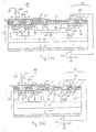
- Fig. 1 is a sectional view of a first embodiment of the present invention.
- an epitaxial wafer which has an N+-substrate 1 of 440 ⁇ m in thickness and an N-type epitaxial layer 13 of 25 ⁇ m in thickness stacked thereon.
- This epitaxial wafer is the same as that employed to manufacture discrete vertical MOSFETs.
- the thickness of the epitaxial layer 13 before impurity diffusion carried out to form a relatively deep P-type diffused region 12 is set so as to be greater than that in the case of manufacturing discrete vertical MOSFETs, because when the deep P-type diffused region 12 is formed subsequently, diffusion of an impurity from the N+-substrate 1 takes place to form an N+ raised region 2, resulting in a reduction in the effective thickness of the epitaxial film 13.
- the semiconductor devices for motorcars are ordinarily required to have a breakdown voltage of about 60 V
- the resistivity of the epitaxial layer 13 is set at about 1 ⁇ cm. In this case, the thickness of the epitaxial layer 13 required before the impurity diffusion for the P-type diffused layer 12 is about 20 to 30 ⁇ m.
- Boron is introduced into the region between a vertical MOSFET 23 and a control circuit 26 by iron implantation or the like and impurity diffusion is carried out at high temperature to form a deep P-type diffused region 12 for isolation.
- impurity diffusion carried out at high temperature for a long period of time, diffusion of an impurity from the N+-substrate 1 takes place to form an N+ raised region 2.
- the thickness of the epitaxial film 13 and the impurity diffusion time for the P-type diffused region 12 are set so that the P-type diffused region 12 for isolation nearly contacts the N+ raised region 2.
- an N+ raised region 2 of about 13 ⁇ m in thickness is formed by carrying out impurity diffusion at 1200°C for 50 hours.
- concentration of implanted boron ions is set at 1.5 x 1013 cm ⁇ 3
- the depth of the P-type diffused region 12 is about 11 ⁇ m.
- a gate oxide film 8 and a polysilicon gate electrode 10 thereon are selectively formed on the N ⁇ epitaxial layer 3 on the left-hand side of the P-type diffused region 12, are selectively formed a gate oxide film 8 and a polysilicon gate electrode 10 thereon.
- This polysilicon gate electrode 10 is covered by a phosphosilicate glass (PSG) film 11.
- PSG phosphosilicate glass
- P-type impurity is diffused into the N ⁇ epitaxial layer 3 to form a P-base region 5 of 3 ⁇ m in depth and N-type impurity is also diffused into the P-base region 5 to form an N+ source region 6.
- This N+ source region 6 is connected to a source electrode 16.
- the P-base region 5 is also connected to the source electrode 16 by a P+ diffused region 7.
- the P-type diffused region 12 is connected with the source electrode 16 through a hole formed in a field oxide film 9 and by using the P+ diffused region 7.
- a drain electrode 14 is formed on
- a P-channel type lateral MOSFET 24 and an N-channel type lateral MOSFET 25 are formed to constitute a CMOS control circuit 26.
- a polysilicon gate 10 is formed on the gate oxide film 8 and P+ diffused region 7 of 1 ⁇ m in depth are formed on both sides of the polysilicon gate 10 to constitute the P-channel type MOSFET 24.
- the P+ diffused region 7 on the right-hand side and the left-hand side are connected to a drain electrode 17 and a source electrode 19, respectively.
- the N ⁇ epitaxial layer 3 is also connected to the source electrode 19 by the N+ diffused region 6 of 1 ⁇ m in depth.
- a polysilicon gate 10 is formed on the gate oxide film 8 and N+ diffused regions 6 of 1 ⁇ m in depth on both sides of the polysilicon gate 10 are formed in the P-well 4 of 6 ⁇ m in depth to constitute the N-channel type MOSFET 25.
- the N+ diffused regions 6 on the left-hand side and the right-hand side are connected to a drain electrode 20 and a source electrode 22, respectively.
- the P-well is also connected to the source electrode 22 by a P+ diffused region 7 of 1 ⁇ m in depth.
- the N+ diffused region 6 used in the N-channel type MOSFET 25 and the P-channel type MOSFET 24 and the N+ diffused region 6 used in the vertical MOSFET 23 are formed simultaneously, the P+ diffused region 7 used in the P-channel type MOSFET 24 and the N-channel type MOSFET 25, the P+ diffused region 7 in the P-type diffused region 12 and the P+ diffused region 7 used in the vertical MOSFET 23 being also formed simultaneously.
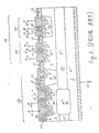
- Fig. 2(a) is a sectional view of an integrated circuit device which has a relatively shallow P-type diffused region 12 between a vertical MOSFET 23 and a control circuit 26.
- illustration of the N-channel type MOSFET 25 shown in Fig. 1 is omitted. Since the device shown in Fig. 2(a) is a high-side switch, the drain 14 of the vertical MOSFET 23 and the source 19 of the P-channel MOSFET 24 are connected to a power supply 35, while the source 16 of the vertical MOSFET 23 is connected to a load resistor 34.
- the base of a parasitic bipolar transistor 33 and the epitaxial resistance 30 of the vertical MOSFET 23 are connected together by an epitaxial resistance 31 below the shallow P-type diffused region 12.
- the output current of the vertical MOSFET 23 increases, the voltage drop across the epitaxial resistance 30 of the vertical MOSFET 23 increases.
- the base of the parasitic bipolar transistor 33 is biased negative with respect to the emitter thereof, thus causing the parasitic transistor 33 to turn on. A current flowing at this time triggers latch-up of the control circuit 26.
- the output current of the vertical MOSFET 23 has no effect on the control circuit 26 since the deep P-type diffused region 12 is elongated so as to nearly reach the N+ raised region 2.
- the base of the parasitic bipolar transistor 33 is connected to the N+ raised region 2 through the base resistance 32.
- This N+ raised region 2 which has a relatively high impurity, concentration, is constantly biased to the power supply voltage V DD . Accordingly, there is no possibility of the parasitic bipolar transistor 33 turning on.
- the structure shown in Fig. 2(b) has no increase in the chip area.
- the depth of the P-type diffused region 12 is about 11 ⁇ m, as described above.
- the width of the deep P-type diffused region 12 is set at 15 ⁇ m or more, it is possible to avoid latch-up of the control circuit 26. It should be noted that even when the deep P-type diffused region 12 is in contact with the N+ raised region 2, the breakdown voltage is unlikely to be lowered because the PN junction is a graded junction. With the above-described diffusion conditions, a breakdown voltage of about 180 V is obtained, so that there is no particular problem in practical application.
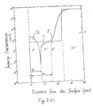
- Figs. 2(c) to 2(e) are diagrams showing impurity distribution profiles under the P-type diffused region 12 obtained by a computer simulation.
- Fig. 2(c), 2(d) and 2(e) show the impurity distribution profiles before formation of the P-type diffused region 12, after diffusion of P-type diffused region 12 for 750 minutes and after diffusion of P-type diffused region 12 for 3000 minutes, respectively. The diffusion is carried out at 1200°C and in an inert gas atmosphere.
- the N+-substrate 1 Since the N+-substrate 1 is connected to the drain electrode 14, its resistivity is selected to be 0.006 to 0.030 ⁇ cm for ohmic contact. This resistivity corresponds to the impurity concentration of 1018 to 1019 cm ⁇ 3. Antimony (Sb) is used as the N-type impurity because of its relatively small diffusion constant.
- the epitaxial layer 13 of 1.0 ⁇ cm in resistivity (5.6 x 1015 cm ⁇ 3 in impurity concentration) and of 25 ⁇ m in film thickness is formed on the N+-substrate 1.
- Phosphorus (P) is used as a dopant for this epitaxial layer 13.
- Fig. 2(c) shows the impurity distribution profiles at this manufacturing step.
- Fig. 2(d) shows the impurity distribution profile after implantation of Boron (B) at the dosage of 1.5 x 1013 cm ⁇ 2 and the diffusion of Boron for 750 minutes at 1200°C and in an inert gas atmosphere
- Fig. 2(e) shows the impurity profile after diffusion for 3,000 minutes.
- a distance of a PN junction from the surface of the epitaxial layer 13 is denoted by xj.
- a notation xe of an effective film thickness of the epitaxial layer 2 denotes the distance from the surface of the region where the impurity concentration of the N-region is equal to that of the initial epitaxial layer 13.
- xj when the diffusion time is 3,000 minutes, xj is 10.4 ⁇ m, xe being 15.9 ⁇ m and the ratio of xj to xe is about 80%.
- the ratio of xj to xe is larger than 0.7 (xj/xe >0.7)
- the impurity concentration of the N ⁇ region 3 between the P-type diffused region 12 and the N+ raised region 2 becomes considerably lower than that of the initial epitaxial layer 13 Consequently, the resistance 31 below the P-type diffused region 12 shown in Fig. 2(a) becomes very large and the base resistance 32 of the parasitic bipolar transistor 33 can be ignored. Accordingly, the parasitic bipolar transistor 33 does not turn on and latch-up can be prevented.
- the impurity concentration of the N+ substrate 1 is favorably from 1017 to 1020 cm ⁇ 3 for the ohmic contact with the drain electrode 14.
- the thickness of the N+ substrate 1 is favorably from 200 to 900 ⁇ m to prevent the wafer from cracking.
- the film thickness and the impurity concentration of the epitaxial layer 13 before the formation of the P+-type diffused region 12 is favorably from 20 to 30 ⁇ m and from 1015 to 1016, respectively, to obtain the large breakdown voltage of 50 to 250 V.
- the distance of the P-type diffused region 12 from the surface is favorably from 5 to 20 ⁇ m, the width thereof being favorably equal to or more than 10 ⁇ m and the impurity concentration of the surface thereof is favorably from 1015 to 1016.
- the thickness of the N+ raised region 2 is favorably from 5 to 25 ⁇ m.
- the film thickness of the epitaxial layer 13 before formation of the P-type diffused region 12 and the thickness of the N+ raised region 2 are denoted by xj, xepi and x N , respectively, the relation among xj, xepi and x N is favorably xj/(xepi-x N )> 0.7, to prevent latch-up by enlarging the resistance 31 under the P-type diffused region 12.
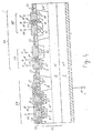
- Figs. 3 and 4 are sectional views of a second and a third embodiments of the present invention, respectively.
- a P-well 40 for an N-channel MOS transistor 25 is formed simultaneously with deep P-type diffused region 12 for isolation. Therefore, it is possible to reduce the number of manufacturing steps.
- the P-type diffused region 12 is relatively deep (for example, about 10 ⁇ m), it is possible to form high-voltage N-channel MOSFETs, 3.g., an offset gate type N-channel MOSFET such as that shown in Fig. 3 and a double-doped drain (DDD) type N-channel MOSFET such as that shown in Fig. 4.
- an N+-type diffused region 6 is formed in an N-type diffused region 41 of 3 ⁇ m in depth and a shallow N ⁇ region 42 of 0.5 ⁇ m in depth is formed between the N-type diffused region 41 and the gate electrode 10 to form the offset gate type N-channel MOSFET 25.
- a P-type diffused region 7 is formed in an P-type diffused region 43 of 3.0 ⁇ m in depth and a shallow P ⁇ region 44 of 0.5 ⁇ m is depth is formed between the P-type diffused region 43 and the gate electrode 10 to form an offset gate type P-channel MOSFET 24.
- an N-type diffused region 41 of 3.0 ⁇ m in depth and an N+-type diffused region 6 of 1.0 ⁇ m in depth are doubly diffused to form a double-doped drain type N-channel MOSFET 25
- an P-type diffused region 43 of 3.0 ⁇ m in depth and P+-type diffused region 7 of 1.0 ⁇ m in depth being doubly diffused to form a double-doped drain type P-channel MOSFET 24.
- the depth of the drain diffused region 41 is increased to be, for example, 3 ⁇ m in order to reduce the strength of the electric field at the drain and thereby achieve a high-voltage device, no punch-through phenomenon occurs between the drain diffused region 41 and the N-type substrate since the P-type diffused region 40 is satisfactorily as deep as 10 ⁇ m.
Landscapes
- Engineering & Computer Science (AREA)
- Power Engineering (AREA)
- Physics & Mathematics (AREA)
- Condensed Matter Physics & Semiconductors (AREA)
- General Physics & Mathematics (AREA)
- Computer Hardware Design (AREA)
- Microelectronics & Electronic Packaging (AREA)
- Manufacturing & Machinery (AREA)
- Metal-Oxide And Bipolar Metal-Oxide Semiconductor Integrated Circuits (AREA)
Abstract
Description
- The present invention relates to a semiconductor device and, more particularly, to a semiconductor device having a plurality of circuit elements including a vertical MOSFET isolated from the other circuit elements.
- Recently, vertical MOSFET's have been employed as switching devices for driving loads, such as lamps and solenoid relays. There has recently been proposed an integrated circuit device wherein a vertical MOSFET and a plurality of peripheral circuit elements are integrated on the same one chip by making use of the advantages that the process for manufacturing a vertical MOSFET and a CMOS IC on the same chip is developed and that various kinds of protecting circuits such as a current-limiting circuit, an overheating-detection circuit, an overvoltage-detection circuit are put into practice by using these peripheral circuit elements to protect the vertical MOSFET from a large current due to a short-circuitting of its load or an application of a high-voltage surge.
- In the integrated circuit device having a vertical MOSFET as an output transistor and other circuit elements formed on the same chip, the vertical MOSFET must be isolated from the other circuit elements. A junction isolation, and a dielectric isolation are examples of the isolation structure in the prior art.
- Fig. 5 shows the junction isolation structure in a prior art (see IEEE 1987 CUSTOM INTEGRATED CIRCUIT CONFERENCE, p. 276), while Fig. 6 shows the dielectric isolation structure in another prior art (see Japanese Patent Laid-Open No. 196576/1986). These conventional isolation structures suffer, however, from the disadvantage that the manufacturing process is complicated and the production cost is high.
- For example, in the junction isolation structure shown in Fig. 5, after an N⁺ buried layer 51 is provided in an N⁺-
substrate 1, a P-typeepitaxial layer 52 and an N-typeepitaxial layer 3 are stacked thereon successively. Then, a P-type impurity is diffused into the N-typeepitaxial layer 3 from the surface to form a P-type diffusedlayer 53 for isolation. Thus, this structure requires a complicated process. - In the dielectric isolation structure shown in Fig. 6, after the bottom surface of an N⁺-
substrate 63 is oxidized to form aninternal oxide film 62 for isolation, theinternal oxide film 62 in a region where avertical MOSFET 23 is to be formed is partially etched away. Then, an N⁺polysilicon layer 61 is deposited on the bottom surface of the N⁺-substrate 63, followed by growing an N⁻epitaxial layer 3 on the upper surface of the N⁺-substrate 63. Finally a trench 64 is provided to effect isolation by filling phosphosilicate glass (PSG) 11. This structure requires to effect alignment between the obverse and reverse sides of thesubstrate 63 and to provide the trench 64 having a relatively deep depth. Thus, the manufacturing process includes technically difficult steps. - As shown in Figs. 5
anc 6, vertical MOSFET uses the N⁺-substrate substrate CMOS circuit portion 26 and the potential at a well 4 need to be fixed. Therefore, the substrate and the well forother circuit portion 26 must be isolated from the drain region of the vertical MOSFET. Accordingly, it is necessary to electrically isolate the vertical MOSFET from the other circuit elements by use of an isolation structure such as the above-described junction isolation or dielectric isolation. - On the other hand, in automotive electrical circuits, the automobile body itself is used as a grounding electrode with a view to reducing the number of interconnections. In the case where the loads such as lamps and solenoid relays in motorcars are driven by using the vertical MOSFET, the loads are connected with the automobile body for preventing them from breaking down by a surge voltage introduced into the positive power line by sparking in engine. This results in an connection of the vertical MOSFET operating as switching devices for driving these loads between those load and the positive power source line. This type of switching device is known as a high-side switch.
- The high-side switch may be formed by using an N-channel vertical MOSFET. The drain of the N-channel MOSFET is connected to the positive power supply side and the source thereof is employed to constitute an output terminal which is connected to a electrode of a power load such as a lamp and a solenoid relay for motorcars.
- As described above, in the high-side switch, the output terminal is connected to the source electrode and the potential at the drain electrode is fixed to a power supply voltage which is common to the other circuit elements. Therefore, it is possible to form a vertical MOSFET and the other circuit elements on a common substrate. However, since the vertical MOSFET used as an output transistor is employed to switch a high voltage and a large current, a large current flows between the source of the vertical MOSFET and the drain region thereof which is common to the substrate of the other circuit elements, resulting in changing the substrate potential. If the substrate potential near the other circuit element lowers, the PN junction between the substrate and source or drain region becomes forward bias to cause latch-up in the portion of the other circuit. Accordingly, a current path must be limited so that there is no adverse effect on the other circuit elements by contriving the device structure. In this case, the device structure must also be contrived to reduce the required numbers of manufacturing steps for easiness of manufacture and low production cost.
- It is, therefore, a major object of the present invention to provide a semiconductor device in which a vertical MOSFET and other circuit elements are formed on a common substrate of a same chip with a simple device structure for manufacturing the device with low cost.
- The semiconductor device in accordance with the present invention includes a semiconductor substrate of one conductivity type, a first electrode formed on an upper surface of the semiconductor substrate, a second electrode formed on a bottom surface of the semiconductor substrate, a switching device for switching a current flowing between the first electrode and the second electrode,
at least one circuit element formed in the upper surface of the semiconductor substrate, and a diffused region of the other conductivity type formed between the switching device and the circuit element. - The at least one circuit element favorably forms a control circuit of the switching device using a complementary MOS circuit. The switching device and the circuit element are favorably an N-channel type vertical MOSFET and a lateral MOSFET, respectively, and the semiconductor substrate favorably has an N-type semiconductor layer in the upper surface thereof, an N-type source and a P-type base of the N-channel type vertical MOSFET and a source and a drain of the lateral MOSFET being formed in the N-type semiconductor layer, and a depth xj of a PN junction between the P-type diffused region and the N-type semiconductor substrate and a depth xe of a region where a concentration of the N-type semiconductor substrate under the P-type diffused region is equal to that of the N-type semiconductor layer having a relation of xj /xe >0.7.
- Unlike the prior art in which a vertical MOSFET is electrically isolated from other circuit element, the present invention employs a relatively deep P-type diffused layer to limit the output current path of the vertical MOSFET, thereby reducing the effect on the other circuit elements, and thus simplifying the device structure as well as facilitating the manufacturing process.
- The above and further objects, features and advantages of the present invention will become more apparent from the following detailed description taken in conjunction with the accompanying drawings, wherein:
- Fig. 1 is a sectional view for explaining a first embodiment of the present invention;
- Figs. 2(a) and 2(b) are sectional views for explaining a first embodiment of the present invention and respectively showing a structure which has a relatively shallow P-type diffused region and a structure which has a relatively deep P-type diffused region;
- Figs. 2(c) to 2(e) are diagrams showing impurity distribution profiles for explaining the present invention;
- Figs. 3 and 4 are sectional views respectively showing a second and a third embodiments of the present invention;
- Fig. 5 is a sectional view showing junction isolation structure of the prior art; and
- Fig. 6 is a sectional view showing a dielectric isolation structure of the prior art.
- Fig. 1 is a sectional view of a first embodiment of the present invention. In this embodiment, is used an epitaxial wafer which has an N⁺-
substrate 1 of 440 µm in thickness and an N-typeepitaxial layer 13 of 25 µm in thickness stacked thereon. This epitaxial wafer is the same as that employed to manufacture discrete vertical MOSFETs. However, the thickness of theepitaxial layer 13 before impurity diffusion carried out to form a relatively deep P-type diffusedregion 12 is set so as to be greater than that in the case of manufacturing discrete vertical MOSFETs, because when the deep P-type diffusedregion 12 is formed subsequently, diffusion of an impurity from the N⁺-substrate 1 takes place to form an N⁺ raisedregion 2, resulting in a reduction in the effective thickness of theepitaxial film 13. Since the semiconductor devices for motorcars are ordinarily required to have a breakdown voltage of about 60 V, the resistivity of theepitaxial layer 13 is set at about 1 Ω·cm. In this case, the thickness of theepitaxial layer 13 required before the impurity diffusion for the P-type diffusedlayer 12 is about 20 to 30 µm. - Boron is introduced into the region between a
vertical MOSFET 23 and acontrol circuit 26 by iron implantation or the like and impurity diffusion is carried out at high temperature to form a deep P-type diffusedregion 12 for isolation. As a result of the impurity diffusion carried out at high temperature for a long period of time, diffusion of an impurity from the N⁺-substrate 1 takes place to form an N⁺ raisedregion 2. The thickness of theepitaxial film 13 and the impurity diffusion time for the P-type diffusedregion 12 are set so that the P-type diffusedregion 12 for isolation nearly contacts the N⁺ raisedregion 2. When an epitaxial wafer which has anepitaxial layer 13 of 1 Ω·cm in resistivity and of 25 µm in film thickness before impurity diffusion is used, an N⁺ raisedregion 2 of about 13 µm in thickness is formed by carrying out impurity diffusion at 1200°C for 50 hours. When the concentration of implanted boron ions is set at 1.5 x 10¹³ cm⁻³, the depth of the P-type diffusedregion 12 is about 11 µm. Thereafter, thevertical MOSFET 23 and thecontrol circuit 26 are formed. - On the N⁻
epitaxial layer 3 on the left-hand side of the P-type diffusedregion 12, are selectively formed agate oxide film 8 and apolysilicon gate electrode 10 thereon. Thispolysilicon gate electrode 10 is covered by a phosphosilicate glass (PSG)film 11. Using thepolysilicon gate electrode 10 as a diffusion mask, P-type impurity is diffused into the N⁻epitaxial layer 3 to form a P-base region 5 of 3 µm in depth and N-type impurity is also diffused into the P-base region 5 to form an N⁺source region 6. This N⁺source region 6 is connected to asource electrode 16. The P-base region 5 is also connected to thesource electrode 16 by a P⁺ diffusedregion 7. The P-type diffusedregion 12 is connected with thesource electrode 16 through a hole formed in afield oxide film 9 and by using the P⁺ diffusedregion 7. Adrain electrode 14 is formed on a bottom surface of the N⁺substrate 1. - In the N⁻
epitaxial layer 3 on the right-hand side of the P-type diffusedregion 12, a P-channeltype lateral MOSFET 24 and an N-channeltype lateral MOSFET 25 are formed to constitute aCMOS control circuit 26. Apolysilicon gate 10 is formed on thegate oxide film 8 and P⁺ diffusedregion 7 of 1 µm in depth are formed on both sides of thepolysilicon gate 10 to constitute the P-channel type MOSFET 24. The P⁺ diffusedregion 7 on the right-hand side and the left-hand side are connected to adrain electrode 17 and asource electrode 19, respectively. The N⁻epitaxial layer 3 is also connected to thesource electrode 19 by the N⁺ diffusedregion 6 of 1 µm in depth. - A
polysilicon gate 10 is formed on thegate oxide film 8 and N⁺ diffusedregions 6 of 1 µm in depth on both sides of thepolysilicon gate 10 are formed in the P-well 4 of 6 µm in depth to constitute the N-channel type MOSFET 25. The N⁺ diffusedregions 6 on the left-hand side and the right-hand side are connected to adrain electrode 20 and asource electrode 22, respectively. The P-well is also connected to thesource electrode 22 by a P⁺ diffusedregion 7 of 1 µm in depth. The N⁺ diffusedregion 6 used in the N-channel type MOSFET 25 and the P-channel type MOSFET 24 and the N⁺ diffusedregion 6 used in thevertical MOSFET 23 are formed simultaneously, the P⁺ diffusedregion 7 used in the P-channel type MOSFET 24 and the N-channel type MOSFET 25, the P⁺ diffusedregion 7 in the P-type diffusedregion 12 and the P⁺ diffusedregion 7 used in thevertical MOSFET 23 being also formed simultaneously. - Fig. 2(a) is a sectional view of an integrated circuit device which has a relatively shallow P-type diffused
region 12 between avertical MOSFET 23 and acontrol circuit 26. In this figure, illustration of the N-channel type MOSFET 25 shown in Fig. 1 is omitted. Since the device shown in Fig. 2(a) is a high-side switch, thedrain 14 of thevertical MOSFET 23 and thesource 19 of the P-channel MOSFET 24 are connected to apower supply 35, while thesource 16 of thevertical MOSFET 23 is connected to aload resistor 34. Since the P-type diffusedregion 12 is shallow, the base of a parasiticbipolar transistor 33 and theepitaxial resistance 30 of thevertical MOSFET 23 are connected together by anepitaxial resistance 31 below the shallow P-type diffusedregion 12. As the output current of thevertical MOSFET 23 increases, the voltage drop across theepitaxial resistance 30 of thevertical MOSFET 23 increases. As a result, the base of the parasiticbipolar transistor 33 is biased negative with respect to the emitter thereof, thus causing theparasitic transistor 33 to turn on. A current flowing at this time triggers latch-up of thecontrol circuit 26. It is necessary, in order to avoid latch-up, to widen the width of the shallow P-type diffusedregion 12 to thereby make theepitaxial resistance 31 below the shallow P-type diffusedregion 12 greater than that of thebase resistance 32 of the parasiticbipolar transistor 33. However, this leads to an increase in the chip area. - On the other hand, in the structure shown in Fig. 2(b), the output current of the
vertical MOSFET 23 has no effect on thecontrol circuit 26 since the deep P-type diffusedregion 12 is elongated so as to nearly reach the N⁺ raisedregion 2. The base of the parasiticbipolar transistor 33 is connected to the N⁺ raisedregion 2 through thebase resistance 32. This N⁺ raisedregion 2, which has a relatively high impurity, concentration, is constantly biased to the power supply voltage VDD. Accordingly, there is no possibility of the parasiticbipolar transistor 33 turning on. Unlike the structure of Fig. 2(a) in which the P-type diffusedregion 12 is shallow, the structure shown in Fig. 2(b) has no increase in the chip area. - In the case where the resistivity and thickness of the
epitaxial layer 13 before the diffusion of the P-type region 12 are 1 Ω·cm and 25 µm, respectively, the depth of the P-type diffusedregion 12 is about 11 µm, as described above. In this case, if the width of the deep P-type diffusedregion 12 is set at 15 µm or more, it is possible to avoid latch-up of thecontrol circuit 26. It should be noted that even when the deep P-type diffusedregion 12 is in contact with the N⁺ raisedregion 2, the breakdown voltage is unlikely to be lowered because the PN junction is a graded junction. With the above-described diffusion conditions, a breakdown voltage of about 180 V is obtained, so that there is no particular problem in practical application. - Figs. 2(c) to 2(e) are diagrams showing impurity distribution profiles under the P-type diffused
region 12 obtained by a computer simulation. Fig. 2(c), 2(d) and 2(e) show the impurity distribution profiles before formation of the P-type diffusedregion 12, after diffusion of P-type diffusedregion 12 for 750 minutes and after diffusion of P-type diffusedregion 12 for 3000 minutes, respectively. The diffusion is carried out at 1200°C and in an inert gas atmosphere. - Since the N⁺-
substrate 1 is connected to thedrain electrode 14, its resistivity is selected to be 0.006 to 0.030 Ω·cm for ohmic contact. This resistivity corresponds to the impurity concentration of 10¹⁸ to 10¹⁹ cm⁻³. Antimony (Sb) is used as the N-type impurity because of its relatively small diffusion constant. Theepitaxial layer 13 of 1.0 Ω·cm in resistivity (5.6 x 10¹⁵ cm⁻³ in impurity concentration) and of 25 µm in film thickness is formed on the N⁺-substrate 1. Phosphorus (P) is used as a dopant for thisepitaxial layer 13. Fig. 2(c) shows the impurity distribution profiles at this manufacturing step. - Fig. 2(d) shows the impurity distribution profile after implantation of Boron (B) at the dosage of 1.5 x 10¹³ cm⁻² and the diffusion of Boron for 750 minutes at 1200°C and in an inert gas atmosphere, and Fig. 2(e) shows the impurity profile after diffusion for 3,000 minutes.
- Here, a distance of a PN junction from the surface of the
epitaxial layer 13 is denoted by xj. A notation xe of an effective film thickness of theepitaxial layer 2 denotes the distance from the surface of the region where the impurity concentration of the N-region is equal to that of theinitial epitaxial layer 13. - Referring to Fig. 2(d), when the diffusion is carried out for 750 minutes, xj is 7.9 µm,xe being 15.9 µm and the ratio of xj to xe is as small as 50%. As a result, the concentration of the N⁻
region 3 between the P-type diffusedregion 12 and the N⁺ raisedregion 2 is almost equal to that of theinitial epitaxial layer 13. Consequently, theresistance 31 under the P-type diffusedregion 12 shown in Fig. 2(a) becomes nearly equal to theresistance 32 of the parasiticbipolar transistor 33 to turn on theparasitic transistor 33, resulting in latch-up. - Referring to Fig. 2(e), when the diffusion time is 3,000 minutes, xj is 10.4 µm, xe being 15.9 µm and the ratio of xj to xe is about 80%. When the ratio of xj to xe is larger than 0.7 (xj/xe >0.7), the impurity concentration of the N⁻
region 3 between the P-type diffusedregion 12 and the N⁺ raisedregion 2 becomes considerably lower than that of theinitial epitaxial layer 13 Consequently, theresistance 31 below the P-type diffusedregion 12 shown in Fig. 2(a) becomes very large and thebase resistance 32 of the parasiticbipolar transistor 33 can be ignored. Accordingly, the parasiticbipolar transistor 33 does not turn on and latch-up can be prevented. - The impurity concentration of the N⁺
substrate 1 is favorably from 10¹⁷ to 10²⁰ cm⁻³ for the ohmic contact with thedrain electrode 14. The thickness of the N⁺substrate 1 is favorably from 200 to 900 µm to prevent the wafer from cracking. - The film thickness and the impurity concentration of the
epitaxial layer 13 before the formation of the P⁺-type diffusedregion 12 is favorably from 20 to 30 µm and from 10¹⁵ to 10¹⁶, respectively, to obtain the large breakdown voltage of 50 to 250 V. - The distance of the P-type diffused
region 12 from the surface is favorably from 5 to 20 µm, the width thereof being favorably equal to or more than 10 µm and the impurity concentration of the surface thereof is favorably from 10¹⁵ to 10¹⁶. The thickness of the N⁺ raisedregion 2 is favorably from 5 to 25 µm. - Additionally, when the depth of the P-type diffused
region 12, the film thickness of theepitaxial layer 13 before formation of the P-type diffusedregion 12 and the thickness of the N⁺ raisedregion 2 are denoted by xj, xepi and xN, respectively, the relation among xj, xepi and xN is favorably xj/(xepi-xN)> 0.7, to prevent latch-up by enlarging theresistance 31 under the P-type diffusedregion 12. - Figs. 3 and 4 are sectional views of a second and a third embodiments of the present invention, respectively. In these embodiments, a P-well 40 for an N-
channel MOS transistor 25 is formed simultaneously with deep P-type diffusedregion 12 for isolation. Therefore, it is possible to reduce the number of manufacturing steps. - Since the P-type diffused
region 12 is relatively deep (for example, about 10 µm), it is possible to form high-voltage N-channel MOSFETs, 3.g., an offset gate type N-channel MOSFET such as that shown in Fig. 3 and a double-doped drain (DDD) type N-channel MOSFET such as that shown in Fig. 4. In Fig. 3, an N⁺-type diffusedregion 6 is formed in an N-type diffusedregion 41 of 3 µm in depth and a shallow N⁻region 42 of 0.5 µm in depth is formed between the N-type diffusedregion 41 and thegate electrode 10 to form the offset gate type N-channel MOSFET 25. A P-type diffusedregion 7 is formed in an P-type diffusedregion 43 of 3.0 µm in depth and a shallow P⁻region 44 of 0.5 µm is depth is formed between the P-type diffusedregion 43 and thegate electrode 10 to form an offset gate type P-channel MOSFET 24. In Fig. 4, an N-type diffusedregion 41 of 3.0 µm in depth and an N⁺-type diffusedregion 6 of 1.0 µm in depth are doubly diffused to form a double-doped drain type N-channel MOSFET 25, an P-type diffusedregion 43 of 3.0 µm in depth and P⁺-type diffusedregion 7 of 1.0 µm in depth being doubly diffused to form a double-doped drain type P-channel MOSFET 24. Even if the depth of the drain diffusedregion 41 is increased to be, for example, 3 µm in order to reduce the strength of the electric field at the drain and thereby achieve a high-voltage device, no punch-through phenomenon occurs between the drain diffusedregion 41 and the N-type substrate since the P-type diffusedregion 40 is satisfactorily as deep as 10 µm.
Claims (12)
a semiconductor substrate of one conductivity type;
a first electrode formed on an upper surface of said semiconductor substrate;
a second electrode formed on a bottom surface of said semiconductor substrate;
a switching device for switching a current flowing between said first electrode and said second electrode;
at least one circuit element formed in said upper surface of said semiconductor substrate; and
a diffused region of the other conductivity type formed between said switching device and said circuit element.
a semiconductor substrate of one conductivity type having a front surface and a back surface;
a first electrode formed on said front surface of said semiconductor substrate to be connected to a first power line of a first power voltage through a load;
a second electrode formed on said back surface of said semiconductor substrate to be connected to a second power line of a second power voltage;
a switching device for switching a current flowing between said first electrode and said second electrode;
a control circuit formed in said front surface of said semiconductor substrate for controlling said switching device; and
a diffused region of the other conductivity type formed between said switching device and said control circuit.
Applications Claiming Priority (2)
| Application Number | Priority Date | Filing Date | Title |
|---|---|---|---|
| JP272223/87 | 1987-10-27 | ||
| JP27222387 | 1987-10-27 |
Publications (3)
| Publication Number | Publication Date |
|---|---|
| EP0314465A2 true EP0314465A2 (en) | 1989-05-03 |
| EP0314465A3 EP0314465A3 (en) | 1991-07-03 |
| EP0314465B1 EP0314465B1 (en) | 1998-05-06 |
Family
ID=17510829
Family Applications (1)
| Application Number | Title | Priority Date | Filing Date |
|---|---|---|---|
| EP88310089A Expired - Lifetime EP0314465B1 (en) | 1987-10-27 | 1988-10-27 | Semiconductor device with an isolated vertical power MOSFET. |
Country Status (3)
| Country | Link |
|---|---|
| US (1) | US5045900A (en) |
| EP (1) | EP0314465B1 (en) |
| DE (1) | DE3856174T2 (en) |
Cited By (6)
| Publication number | Priority date | Publication date | Assignee | Title |
|---|---|---|---|---|
| EP0453070A2 (en) * | 1990-02-23 | 1991-10-23 | Nippon Motorola Ltd. | Method of manufacturing an intelligent power semiconductor device |
| EP0544047A1 (en) * | 1991-11-25 | 1993-06-02 | STMicroelectronics S.r.l. | High current MOS transistor integrated bridge structure optimising conduction power losses |
| EP0643422A1 (en) * | 1993-09-13 | 1995-03-15 | Texas Instruments Incorporated | Method and system for protecting integrated circuits |
| EP0670601A2 (en) * | 1994-03-04 | 1995-09-06 | Fuji Electric Co. Ltd. | Insulated gate-type bipolar transistor |
| WO2001045155A1 (en) * | 1999-12-15 | 2001-06-21 | Koninklijke Philips Electronics N.V. | Manufacture of semiconductor material and devices using that material |
| CN104221148A (en) * | 2012-09-18 | 2014-12-17 | 富士电机株式会社 | Semiconductor device and power conversion apparatus using same |
Families Citing this family (15)
| Publication number | Priority date | Publication date | Assignee | Title |
|---|---|---|---|---|
| USRE34025E (en) * | 1987-02-13 | 1992-08-11 | Kabushiki Kaisha Toshiba | Semiconductor device with isolation between MOSFET and control circuit |
| US5294559A (en) * | 1990-07-30 | 1994-03-15 | Texas Instruments Incorporated | Method of forming a vertical transistor |
| JP3216206B2 (en) * | 1992-03-30 | 2001-10-09 | 株式会社デンソー | Semiconductor device and manufacturing method thereof |
| US5446300A (en) * | 1992-11-04 | 1995-08-29 | North American Philips Corporation | Semiconductor device configuration with multiple HV-LDMOS transistors and a floating well circuit |
| DE4242669C2 (en) * | 1992-12-17 | 2001-09-13 | Hanning Electronic Gmbh & Co | Semiconductor arrangement with a vertical semiconductor power switch and an integrated circuit |
| US5721445A (en) * | 1995-03-02 | 1998-02-24 | Lucent Technologies Inc. | Semiconductor device with increased parasitic emitter resistance and improved latch-up immunity |
| US5510281A (en) * | 1995-03-20 | 1996-04-23 | General Electric Company | Method of fabricating a self-aligned DMOS transistor device using SiC and spacers |
| US5814858A (en) * | 1996-03-15 | 1998-09-29 | Siliconix Incorporated | Vertical power MOSFET having reduced sensitivity to variations in thickness of epitaxial layer |
| JP3527034B2 (en) * | 1996-09-20 | 2004-05-17 | 株式会社半導体エネルギー研究所 | Semiconductor device |
| US5830789A (en) * | 1996-11-19 | 1998-11-03 | Integrated Device Technology, Inc. | CMOS process forming wells after gate formation |
| US6429481B1 (en) | 1997-11-14 | 2002-08-06 | Fairchild Semiconductor Corporation | Field effect transistor and method of its manufacture |
| KR100281908B1 (en) * | 1998-11-20 | 2001-02-15 | 김덕중 | Semiconductor device and manufacturing method |
| US6642577B2 (en) * | 2000-03-16 | 2003-11-04 | Denso Corporation | Semiconductor device including power MOSFET and peripheral device and method for manufacturing the same |
| US7078296B2 (en) | 2002-01-16 | 2006-07-18 | Fairchild Semiconductor Corporation | Self-aligned trench MOSFETs and methods for making the same |
| JP5196794B2 (en) * | 2007-01-29 | 2013-05-15 | 三菱電機株式会社 | Semiconductor device |
Citations (4)
| Publication number | Priority date | Publication date | Assignee | Title |
|---|---|---|---|---|
| GB2168842A (en) * | 1984-09-21 | 1986-06-25 | Sgs Microelettronica Spa | Integrated semiconductor power devices |
| JPS61196576A (en) * | 1985-02-26 | 1986-08-30 | Nissan Motor Co Ltd | Semiconductor device |
| JPS61196568A (en) * | 1985-02-26 | 1986-08-30 | Nissan Motor Co Ltd | Semiconductor device |
| EP0292972A2 (en) * | 1987-05-29 | 1988-11-30 | Nissan Motor Co., Ltd. | IC with recombination layer and guard ring separating VDMOS and CMOS or the like |
Family Cites Families (1)
| Publication number | Priority date | Publication date | Assignee | Title |
|---|---|---|---|---|
| JPH0685441B2 (en) * | 1986-06-18 | 1994-10-26 | 日産自動車株式会社 | Semiconductor device |
-
1988
- 1988-10-27 DE DE3856174T patent/DE3856174T2/en not_active Expired - Fee Related
- 1988-10-27 EP EP88310089A patent/EP0314465B1/en not_active Expired - Lifetime
-
1991
- 1991-01-22 US US07/643,105 patent/US5045900A/en not_active Expired - Fee Related
Patent Citations (4)
| Publication number | Priority date | Publication date | Assignee | Title |
|---|---|---|---|---|
| GB2168842A (en) * | 1984-09-21 | 1986-06-25 | Sgs Microelettronica Spa | Integrated semiconductor power devices |
| JPS61196576A (en) * | 1985-02-26 | 1986-08-30 | Nissan Motor Co Ltd | Semiconductor device |
| JPS61196568A (en) * | 1985-02-26 | 1986-08-30 | Nissan Motor Co Ltd | Semiconductor device |
| EP0292972A2 (en) * | 1987-05-29 | 1988-11-30 | Nissan Motor Co., Ltd. | IC with recombination layer and guard ring separating VDMOS and CMOS or the like |
Non-Patent Citations (2)
| Title |
|---|
| PATENT ABSTRACTS OF JAPAN, vol. 11, no. 27 (E-474)[2474], 27th January 1987; & JP-A-61 196 568 (NISSAN) 30-08-1986 * |
| PATENT ABSTRACTS OF JAPAN, vol. 11, no. 27 (E-474)[2474], 27th January 1987; & JP-A-61 196 576 (NISSAN) 30-08-1986 * |
Cited By (12)
| Publication number | Priority date | Publication date | Assignee | Title |
|---|---|---|---|---|
| EP0453070A2 (en) * | 1990-02-23 | 1991-10-23 | Nippon Motorola Ltd. | Method of manufacturing an intelligent power semiconductor device |
| EP0453070A3 (en) * | 1990-02-23 | 1992-03-11 | Nippon Motorola Ltd. | Method of manufacturing an intelligent power semiconductor device |
| EP0544047A1 (en) * | 1991-11-25 | 1993-06-02 | STMicroelectronics S.r.l. | High current MOS transistor integrated bridge structure optimising conduction power losses |
| EP0643422A1 (en) * | 1993-09-13 | 1995-03-15 | Texas Instruments Incorporated | Method and system for protecting integrated circuits |
| US6208493B1 (en) | 1993-09-13 | 2001-03-27 | Texas Instruments Incorporated | Method and system for protecting integrated circuits against a variety of transients |
| EP0670601A2 (en) * | 1994-03-04 | 1995-09-06 | Fuji Electric Co. Ltd. | Insulated gate-type bipolar transistor |
| EP0670601A3 (en) * | 1994-03-04 | 1995-10-11 | Fuji Electric Co Ltd | |
| US5557128A (en) * | 1994-03-04 | 1996-09-17 | Fuji Electric Co., Ltd. | Insulated-gate type bipolar transistor |
| WO2001045155A1 (en) * | 1999-12-15 | 2001-06-21 | Koninklijke Philips Electronics N.V. | Manufacture of semiconductor material and devices using that material |
| US6495421B2 (en) | 1999-12-15 | 2002-12-17 | Koninklijke Philips Electronics N.V. | Manufacture of semiconductor material and devices using that material |
| CN104221148A (en) * | 2012-09-18 | 2014-12-17 | 富士电机株式会社 | Semiconductor device and power conversion apparatus using same |
| CN104221148B (en) * | 2012-09-18 | 2017-03-15 | 富士电机株式会社 | Semiconductor device and the power conversion device using the semiconductor device |
Also Published As
| Publication number | Publication date |
|---|---|
| DE3856174T2 (en) | 1998-09-03 |
| US5045900A (en) | 1991-09-03 |
| DE3856174D1 (en) | 1998-06-10 |
| EP0314465A3 (en) | 1991-07-03 |
| EP0314465B1 (en) | 1998-05-06 |
Similar Documents
| Publication | Publication Date | Title |
|---|---|---|
| US5045900A (en) | Semiconductor device having a vertical power MOSFET fabricated in an isolated form on a semiconductor substrate | |
| EP0097379B1 (en) | Method for manufacturing semiconductor devices | |
| KR100433691B1 (en) | ESD protection apparatus and method for fabricating the same | |
| US4928159A (en) | Semiconductor device | |
| EP0057024B1 (en) | Semiconductor device having a safety device | |
| EP2421040A1 (en) | A modular bipolar-CMOS-DMOS analog integrated circuit and power transistor technology | |
| US5959332A (en) | Electrostatic-discharge protection device and method for making the same | |
| US6570229B1 (en) | Semiconductor device | |
| JPH10284731A (en) | Dmos transistor having schottky diode body structure | |
| KR920005539B1 (en) | Semiconductor overvoltage suppressor with accurately determined striking potential | |
| KR100208632B1 (en) | Semiconductor integrated circuit and method of fabricating it | |
| US11521961B2 (en) | Back ballasted vertical NPN transistor | |
| JPH0626253B2 (en) | Method of manufacturing semiconductor device including diffusion region having short length | |
| US11869885B2 (en) | Silicon controlled rectifier | |
| JP2680788B2 (en) | Integrated structure active clamp device | |
| EP0630054A1 (en) | Thyristor with insulated gate and method for operating the same | |
| CN114649326A (en) | Insulated gate bipolar transistor with integrated schottky barrier | |
| US6127723A (en) | Integrated device in an emitter-switching configuration | |
| EP0423826A2 (en) | MOS-type integrated circuit | |
| EP0381139A2 (en) | Semiconductor integrated circuit and method of manufacture thereof | |
| US7026705B2 (en) | Semiconductor device with surge protection circuit capable of preventing current leakage | |
| US5773338A (en) | Bipolar transistor with MOS-controlled protection for reverse-biased emitter-based junction | |
| CN111584481A (en) | Transistor structure for electrostatic protection and manufacturing method thereof | |
| JP2729062B2 (en) | Integrated circuit device | |
| US20120112291A1 (en) | Semiconductor Apparatus And Manufacturing Method Thereof |
Legal Events
| Date | Code | Title | Description |
|---|---|---|---|
| PUAI | Public reference made under article 153(3) epc to a published international application that has entered the european phase |
Free format text: ORIGINAL CODE: 0009012 |
|
| 17P | Request for examination filed |
Effective date: 19881112 |
|
| AK | Designated contracting states |
Kind code of ref document: A2 Designated state(s): DE FR GB |
|
| PUAL | Search report despatched |
Free format text: ORIGINAL CODE: 0009013 |
|
| AK | Designated contracting states |
Kind code of ref document: A3 Designated state(s): DE FR GB |
|
| RHK1 | Main classification (correction) |
Ipc: H01L 21/76 |
|
| 17Q | First examination report despatched |
Effective date: 19940321 |
|
| GRAG | Despatch of communication of intention to grant |
Free format text: ORIGINAL CODE: EPIDOS AGRA |
|
| GRAG | Despatch of communication of intention to grant |
Free format text: ORIGINAL CODE: EPIDOS AGRA |
|
| GRAG | Despatch of communication of intention to grant |
Free format text: ORIGINAL CODE: EPIDOS AGRA |
|
| GRAH | Despatch of communication of intention to grant a patent |
Free format text: ORIGINAL CODE: EPIDOS IGRA |
|
| GRAH | Despatch of communication of intention to grant a patent |
Free format text: ORIGINAL CODE: EPIDOS IGRA |
|
| GRAA | (expected) grant |
Free format text: ORIGINAL CODE: 0009210 |
|
| AK | Designated contracting states |
Kind code of ref document: B1 Designated state(s): DE FR GB |
|
| REF | Corresponds to: |
Ref document number: 3856174 Country of ref document: DE Date of ref document: 19980610 |
|
| ET | Fr: translation filed | ||
| PLBE | No opposition filed within time limit |
Free format text: ORIGINAL CODE: 0009261 |
|
| STAA | Information on the status of an ep patent application or granted ep patent |
Free format text: STATUS: NO OPPOSITION FILED WITHIN TIME LIMIT |
|
| 26N | No opposition filed | ||
| PGFP | Annual fee paid to national office [announced via postgrant information from national office to epo] |
Ref country code: FR Payment date: 20011010 Year of fee payment: 14 |
|
| PGFP | Annual fee paid to national office [announced via postgrant information from national office to epo] |
Ref country code: GB Payment date: 20011031 Year of fee payment: 14 |
|
| PGFP | Annual fee paid to national office [announced via postgrant information from national office to epo] |
Ref country code: DE Payment date: 20011112 Year of fee payment: 14 |
|
| REG | Reference to a national code |
Ref country code: GB Ref legal event code: IF02 |
|
| PG25 | Lapsed in a contracting state [announced via postgrant information from national office to epo] |
Ref country code: GB Free format text: LAPSE BECAUSE OF NON-PAYMENT OF DUE FEES Effective date: 20021027 |
|
| PG25 | Lapsed in a contracting state [announced via postgrant information from national office to epo] |
Ref country code: DE Free format text: LAPSE BECAUSE OF NON-PAYMENT OF DUE FEES Effective date: 20030501 |
|
| GBPC | Gb: european patent ceased through non-payment of renewal fee | ||
| PG25 | Lapsed in a contracting state [announced via postgrant information from national office to epo] |
Ref country code: FR Free format text: LAPSE BECAUSE OF NON-PAYMENT OF DUE FEES Effective date: 20030630 |
|
| REG | Reference to a national code |
Ref country code: FR Ref legal event code: ST |