EP0311152B1 - Tone signal generation device for an electronic musical instrument - Google Patents
Tone signal generation device for an electronic musical instrument Download PDFInfo
- Publication number
- EP0311152B1 EP0311152B1 EP88119459A EP88119459A EP0311152B1 EP 0311152 B1 EP0311152 B1 EP 0311152B1 EP 88119459 A EP88119459 A EP 88119459A EP 88119459 A EP88119459 A EP 88119459A EP 0311152 B1 EP0311152 B1 EP 0311152B1
- Authority
- EP
- European Patent Office
- Prior art keywords
- waveshape
- tone
- waveshapes
- interpolation
- segment
- Prior art date
- Legal status (The legal status is an assumption and is not a legal conclusion. Google has not performed a legal analysis and makes no representation as to the accuracy of the status listed.)
- Expired - Lifetime
Links
Images


Classifications
-
- G—PHYSICS
- G10—MUSICAL INSTRUMENTS; ACOUSTICS
- G10H—ELECTROPHONIC MUSICAL INSTRUMENTS; INSTRUMENTS IN WHICH THE TONES ARE GENERATED BY ELECTROMECHANICAL MEANS OR ELECTRONIC GENERATORS, OR IN WHICH THE TONES ARE SYNTHESISED FROM A DATA STORE
- G10H1/00—Details of electrophonic musical instruments
- G10H1/02—Means for controlling the tone frequencies, e.g. attack or decay; Means for producing special musical effects, e.g. vibratos or glissandos
- G10H1/06—Circuits for establishing the harmonic content of tones, or other arrangements for changing the tone colour
- G10H1/08—Circuits for establishing the harmonic content of tones, or other arrangements for changing the tone colour by combining tones
-
- G—PHYSICS
- G10—MUSICAL INSTRUMENTS; ACOUSTICS
- G10H—ELECTROPHONIC MUSICAL INSTRUMENTS; INSTRUMENTS IN WHICH THE TONES ARE GENERATED BY ELECTROMECHANICAL MEANS OR ELECTRONIC GENERATORS, OR IN WHICH THE TONES ARE SYNTHESISED FROM A DATA STORE
- G10H7/00—Instruments in which the tones are synthesised from a data store, e.g. computer organs
- G10H7/008—Means for controlling the transition from one tone waveform to another
Definitions
- the phase generator 13 supplies the cross fade control circuit 16 with an attack end signal ATEND which indicates that the full attack-portion waveshape has been read out and an inverted attack signal AT which indicates that the attack portion has not been read out yet.
- the cross fade control circuit 16 Upon checking the completion of reading of the attack portion based on these signals, the cross fade control circuit 16 starts producing a given interpolation function.
- the interpolation function is produced from the circuit 16 as cross fade curve data CF and supplied to a multiplier 18 provided for weighting operation. Also a waveshape switching command signal WCHG is produced from the circuit 16 and supplied to the phase generator 13.
- the selector 50 selects the data applied to its A input from the last stage of the shift register 51 through the subtractor 48 and supplies the data to the shift register 51.
- the carry-out signal CRY produced by the adder 35 shown in Fig. 5 is applied to the gate 49.
- the gate 49 is enabled by the attack signal AT during the attack to provide the carry-out signal CRY to the subtractor 48.
- the subtractor 48 subtracts "1" from the output data of the shift register 51.
- the data indicating the number of periods of the full attack-portion waveshape is first applied to the shift register 51, thereafter "1" being subtracted from said data each time one period of the attack portion waveshape is read out until finally the reading of the full attack-portion waveshape is completed.
- the AND gate 65 is enabled in response to "1" of the clock pulse ⁇ 2 while the AND gate 66 is not enabled.
- the output of the delay circuit 63 is selected through the A input of the selector 58, to which output "1" is added by the adder 61 in response to the signal WCHG.
- the delay circuit 63 produces data 23 time slots ahead in terms of subchannel timing. This data is the count data of the subchannel 2 in the preceding cycle related to the same channel. The count of the subchannel 2 as added with "1" is the new count.
- the count of the subchannel 2 is greater than that of the subchannel 1 by 1, it is as if the count of the subchannel 1 were added with 2. For instance when, as mentioned, the count of the subchannel 1 is "1" and the count of the subchannel 2 is "2", the count "2" in the previous cycle (i.e., the output of the delay circuit 63) is added with 1 at the timing of the subchannel 1 when the first waveshape switching command signal WCHG is provided in correspondence to the subchannel 1, thus the count of the subchannel 1 changing to "3".
- the output of the function conversion circuit 78 is used as a basic interpolation function IPF2 for the second channel (subchannel 2).
- An inversion circuit 79 is provided to produce another function of the opposite characteristic by inverting each bit of the interpolation function IPF2.
- This function of the opposite characteristics is the basic interpolation function IPF1 for the first channel (subchannel 1).
- Fig. 11, part (c) shows an example of these interpolation functions IPF1, IPF2.
- the output of the function conversion circuit 78 is all 0s because the output of the second counter 73B is all 0s so that the value of the second-channel interpolation function IPF2 maintains the minimum (0) while the first-channel interpolation function IPF1 maintains the maximum.
Description
- This invention relates to a tone signal generation device adapted for use in an electronic musical instrument and other apparatus having a tone generation function and, more particularly, to a tone signal generation device capable of generating a tone signal whose spectrum components change with the lapse of time by successively generating different tone waveshapes as well as capable of generating a tone signal containing a non-harmonic component.
- US-A-4 085 648 describes a tone signal generating device having a first tone signal source (piano version) and a second signal source (forte version). The tone signals of both signal sources are intermixed in an interpolation means that is coupled to an operating member, for example a key. The interpolation means generates a composite signal including all components to synthesize the timbre of piano or forte music. Thereby, it is not necessary to store sound signals representing a plurality of volume levels of sound of a given pitch and the intervening transition areas and to provide means for the selective interrogation of a determined storage region.
- Tones produced by acoustic musical instruments, particularly string-striking musical instruments such as piano and harpsichord, contain components which are not in an exact harmonic relationship of the notes of these tones (i.e., nonharmonic components). Since in the known tone signal generation system in which tone waveshapes stored in a waveshape memory are simply read out repeatedly can produce only harmonics of integer multiples, such known system cannot produce a tone signal containing a nonharmonic component. On the other hand, an electronic musical instrument of a type in which individual harmonic components are separately calculated and synthesized together, synthesis of a tone signal containing nonharmonic components is possible as is disclosed in the specification of US-A-3,888,153. More specifically, a partial tone signal of a nonharmonic component is generated by causing the frequency of each individually generated harmonic component to deviate slightly from an integer multiple of the fundamental frequency as required and then partial tone signals are synthesized with the nonharmonic partial tone signal to provide a tone signal containing a nonharmonic component.
- This prior art device however has the disadvantage that it requires a large-scale hardware because it necessitates a construction in which partial tone signals corresponding to the fundamental wave and respective harmonics must be produced individually and separately and relative amplitudes of these partial tone signals must be individually controlled before synthesizing these signals.
- It is therefore an object of the invention to provide a tone signal generation device capable of readily producing a tone signal containing a nonharmonic component with a relatively simple construction.
- The tone signal generating device according to the invention is defined by
claim 1. - In a preferable embodiment, the function generating means comprises function memory means for storing the first weighting function and function readout means for reading out the first weighting function in a forward direction from the function memory means to generate the first weighting function and for reading out the first weighting function in a reverse direction from said function memory means to generate the second weighting function.
- Since the weighting of the first and second waveshapes are separately made by the first weighting function having the first curve and the second weighting function having the second curve which has the shape reversed the first curve, the first and second waveshapes are weighted by interpolation characteristics which are opposite to each other so that interpolation of symmetrical characteristics which is not partial to either waveshape is ensured regardless of the type of interpolation function (weighting function) employed.
- This will be explained more fully with reference to Figs. 30a and 30b. Fig. 30a shows the prior art interpolation method in which X represents a weighting coefficient which is a desired function (an exponential function in the figure) of X = f(t). A(1 - X) represents the level of a preceding tone waveshape after the interpolation which is indicated by oblique lines rising from left to right. BX represents the level of a following waveshape after the interpolation which is indicated by oblique lines rising from right to left. In this case, it will be understood that interpolation characteristics which is partial to the preceding tone waveshape is obtained. Fig. 30b shows the interpolation method according to the invention in which Y = g(t) represents a function obtained by reading out the function X = f(t) reversely. The preceding tone waveshape is weighted by this function and the level AY after weighting is indicated by oblique lines rising from left to right. The following tone waveshape is weighted by the function X = f(t) and the level BX after weighting is indicated by oblique lines rising from right to left. As will be apparent from Fig. 30b, the two tone waveshapes are symmetrically interpolated without being partial to either one. That is, the level AY first is large and the level BX is small. Then the two levels become equal in the middle and in the latter half section, the level BX is large and the level AY is small in symmetry to the change in the former half section. Accordingly, waveshape switches from one to another smoothly and impartially regardless of the type of the interpolation function. In contrast, in Fig. 30a, the level A(1 - X) is partially large as a whole and the level BX increases immediately before the end of the interpolation so that it is not a very smooth transition.
- According to the invention, each tone waveshape stored in the waveshape memory means contains a fundamental component and harmonics components and, with respect to all or predetermined ones of the respective tone waveshapes, at least one of these components is provided with a phase difference between tone waveshapes which are adjacent to each other in the order of switching, whereby nonharmony determined by this phase difference and time (interpolation time) required for transition of waveshapes by the interpolation means is realized. In other words, the tone signal generation device according to the invention comprises waveshape generating means for generating a first waveshape and a second waveshape whose fundamental frequencies are same, phase difference between Nth harmonics of the first and second waveshapes being provided wherein N is a positive integer, function generating means for generating a weighting function, and interpolation means connected to the waveshape generating means for weighting the first and second waveshapes in accordance with a weighting value representing a value of the weighting function, for combining the weighted waveshapes and for outputting the combined waveshape at a rate corresponding to a frequency of a musical tone to be produced as a tone signal of the musical tone so that the musical tone has a nonharmonic component whose frequency is beside the frequencies of said Nth harmonics.
- The tone signal obtained by the interpolation performed by the interpolation means is not the waveshape itself which is generated by the waveshape generating means but a waveshape which is shifted smoothly from a preceding waveshape (the first) to a following waveshape (the second). The transition of the tone waveshapes can be analized component by component. That is, as to the n-th component, smooth transition from the n-th component of the preceding tone waveshape to the n-th component of the following waveshape is realized. Observing initial phase of the tone waveshape, the initial phase of the tone waveshape obtained by the interpolation changes gradually from the initial phase of the n-th component of the preceding tone waveshape to the initial phase of the n-th component of the following tone waveshape. In this case, as to a component which is not provided with a phase difference between adjacent tone waveshapes, its initial phase does not change during the interpolation. Thus, as to the component which is not provided with a phase difference, a harmonic frequency of integer multiple as indicated by the order number of the harmonic is obtained. As to a component which are provided with a phase difference between adjacent tone waveshapes, its initial phase changes gradually from the initial phase of the preceding tone waveshape to that of the following tone waveshape during the interpolation. By transition of the initial phase of a specific component during the interpolation, the frequency of this component does not become the original frequency of integer multiple but become a frequency which is more or less deviated from it. Thus, this specific component becomes a nonharmonic frequency and a tone signal containing a nonharmonic component thereby is obtained.
- The principle of generation of such nonharmonic frequency will be described in detail with reference to Fig. 31. In Fig. 31, a second harmonic component (represented by SEG1₂) contained in a preceding tone waveshape and a second harmonic component (represented by SEG2₂) contained in a next tone waveshape are taken out and shown. Explanation will be made on a case where a predetermined phase difference has been provided to the second harmonic components. Fig. 31 is drawn in three-dimensional co-ordinates in which the X axis represents phase, the Y axis amplitude and the Z axis time respectively. The start point of the interpolation is represented by t1s and the end point thereof by t1e and it is assumed that a linear interpolation is carried out between t1s and t1e from SEG1₂ to SEG2₂. In the figure, phase difference between the two second harmonics is assumed to be 22.5 degrees.
- Assuming that the fundamental frequency is 440 Hz (corresponding to A4 tone), the frequency of the second harmonic is 880 Hz (1 period being 1.136 ms). Assuming also that the interpolation period from t1s to t1e is set to be 18.182 ms which is equivalent to 16 periods of this second harmonic, if there was no phase difference between these two components SEG1₂ and SEG2₂, a second harmonic of 16 periods would be generated in this interpolation period so that the frequency of the synthesized second harmonic component would be just double that of the fundamental wave. Since, however, there is the phase difference of 22.5 degrees between the components SEG1₂ and SEG2₂, the initial phase of the second harmonic synthesized by the interpolation is gradually shifted so that it is shifted by 22.5 degrees at the interpolation end point t₁e as compared with the phase at the interpolation start point t₁s. The direction of this phase shift is determined by the direction of phase shift to SEG2₂ relative to SEG1₂ which is the direction in which the phase advances in the example illustrated. Since 22.5 degrees corresponds to

period, a second harmonic component having 16.0625 periods during the interpolation period t1s - t1e is produced. Frequency f₂ corresponding to this second harmonic is not exactly 880 Hz which is the frequency of a second harmonic but is
In other words, the second harmonic component is synthesized as a nonharmonic component which is deviated by about 3.44 Hz from the integer multiple frequency. - Nonharmonic components may be synthesized for components of other harmonic orders on the basis of the same principle. If, for example, phase difference of a third harmonic component is 45 degrees in the same condition as the above described case, a frequency f₃ of a synthesized third harmonic component becomes

while a normal integer multiple frequency is 1320 Hz. The period corresponding to the phase difference of 45 degrees is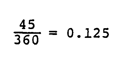
(period). If phase difference of a fourth harmonic component is 90 degrees in the same condition as the above cases, a frequency f₄ of a synthesized fourth harmonic component becomes
The period corresponding to the phase difference of 90 degrees is
(period). Phase difference as described above may be provided not only for harmonic components but also for the fundamental component. In the latter case, a nonharmonic relationship can be produced between a fundamental component which is slightly deviated from a normal frequency and a harmonic component which is not deviated at all. - The present application is applicable not only to a type of device in which a tone waveshape which is an object of interpolation is formed by reading out tone waveshapes from a waveshape memory storing intermittently sampled different tone waveshapes but also advantageously to a type of device in which a tone waveshape is formed by employing parameters. As an example of such tone waveshape forming system employing parameters, the harmonic synthesizing system may be cited. In this harmonic synthesizing system, timewise change in the spectrum of a tone signal has been conventionally effected by preparing many sets of harmonic coefficients setting relative amplitudes of respective harmonics and timewise changing these sets of coefficients to utilize them in a tone waveshape forming operation. This necessitates a memory of a large capacity storing the harmonic coefficients and besides a smooth timewise change in the tone waveshape is not expected. If a parameter type tone forming means is employed in the present invention, timewise change in the tone waveshape by the interpolation according to the invention can be advantageously realized in the harmonic synthesis operation system or other parameter type systems. According to the invention, the waveshape memory and readout means may be replaced by tone waveshape forming means for forming a tone waveshape of a shape determined by a parameter and forming the tone waveshape in according with phase designated by phase data, parameter memory means for storing the parameters determining the shape of respective tone waveshapes with respect to different tone waveshapes which have been intermittently sampled between the start to end of sounding of a tone and phase data generation means for generating the phase data which changes in response to the frequency of the tone to be generated and providing the phase data to the tone waveshape forming means.
- In the accompanying drawings,
- Figs. 1a and 1b are schematic views for explaining the principle of the tone signal generation in an embodiment of the invention;
- Fig. 2 is an electric block diagram showing an embodiment of the electronic musical instrument using the tone signal generation device according to the invention;
- Fig. 3 is a time chart showing an example of a clock pulse and a channel timing signal used in this embodiment;
- Fig. 4 shows an example of the memory map of a waveshape memory in the embodiment;
- Fig. 5 is an electric block diagram showing an example of a phase generator shown in Fig. 2;
- Fig. 6 is an electric block diagram showing a time division control circuit shown in Fig. 5;
- Fig. 7 is a timing chart showing an example each of various signals appearing in Fig. 6;
- Fig. 8 is an electric block diagram showing an example of an attack end detection circuit shown in Fig. 5;
- Fig. 9 is an electric block diagram showing an example of a start address generation circuit shown in Fig. 5;
- Fig. 10 is an electric block diagram showing an example of a cross fade control circuit shown in Fig. 2;
- Fig. 11 is a time chart showing an example each of various signals appearing in Figs. 8, 9 and 10;
- Figs. 12a - 12e are schematic views showing various interpolation functions (cross fade curves) prepared in a cross fade curve memory shown in Fig. 10;
- Figs. 13 to 17 are waveshape diagrams each showing an example of a segment waveshape stored in the waveshape memory shown in Fig. 2, Fig. 13 showing a first switching order segment waveshape SEG1, Fig. 14 showing a second switching order segment waveshape SEG2, Fig. 15 showing a third switching order segment waveshape SEG3, Fig. 16 showing a fourth switching order segment waveshape SEG4, and Fig. 17 showing a fifth switching order segment waveshape SEG5;
- Figs. 18 and 19 are waveshape diagrams showing examples of tone signals synthesized by the embodiment shown in Fig. 2 using the segment waveshapes of Figs. 13 to 17;
- Fig. 20 is a spectrum envelope diagram showing the frequency spectra of the tone signals of Figs. 18 and 19;
- Fig. 21 is a diagram showing the spectrum envelope including the third and fourth harmonics portions;
- Fig. 22 is an electric block diagram showing a modification of a first counter and a change rate memory shown in Fig. 10, namely, counting rate control means;
- Fig. 23 is an electric block diagram showing a modification of a second counter shown in Fig. 10;
- Fig. 24 is an electric block diagram showing a modification of a start address generation circuit shown in Fig. 9;
- Fig. 25 shows an example of interpolation other than that shown in Fig. 1b;
- Fig. 26 is an electric block diagram showing another embodiment of the invention;
- Fig. 27 is an electric block diagram showing an example of a segment order data generation circuit shown in Fig. 26;
- Fig. 28 is a block diagram schematically showing an example of a tone waveshape forming circuit shown in Fig. 26 as constructed by the harmonics synthesizing method;
- Fig. 29 is a block diagram schematically showing an example of a tone waveshape forming circuit by the digital filter method;
- Figs. 30a and 30b show an example of interpolation characteristics for explaining difference between the conventional interpolation and the interpolation according to the invention; and
- Fig. 31 is a waveshape diagram showing waveshapes (especially the phase relation) of same order components respectively contained in two tone waveshapes to be interpolated, for explaining the principle based on which nonharmonic components are generated by the interpolation synthesis according to the invention.
- An embodiment of the present invention will now be described with reference to the accompanying drawings.
- Referring first to Figs. 1a and 1b, description will be made on the principle of the tone signal generation used in the embodiment to be described below. For the sake of convenience, Fig. 1a shows only the amplitude envelope to diagramatically describe the tone waveshape to be prepared in the waveshape memory. Because the tone waveshape changes in a complicated manner for a given period of time from the start of sounding, simulation of a good quality waveshape for the attack portion is difficult when depending on the repetitive reading of a single-period waveshape. Therefore, the attack portion is in intact manner stored in the waveshape memory according to this embodiment. In all the sounding period following the attack portion, one period of a plurality of different tone waveshapes is sampled intermittently and stored in the waveshape memory. Thus a plurality of tone waveshapes are prepared in correspondence to intermittent time periods and stored in the waveshape memory. These plural waveshapes are used in the interpolation operation according to the invention. Fig. 1a shows the intermittently sampled waveshapes of a single period SEG1 to SEG5. These will be called segment waveshapes below for the sake of convenience. The waveshapes stored in the waveshape memory are read out basically as follows: First, the full waveshape of the attack portion is read out continuously, the segment waveshape SEG1 to SEG5 are selected in order at a timing following the waveshape switching command to be described later and the one period of the selected segment waveshapes is read out repeatedly. For instance, when the reading of the attack portion waveshape is completed, the first segment waveshape SEG1 is read repeatedly for a certain period of time and then the second segment waveshape SEG2 is read repeatedly, thus switching one segment waveshape to another thereafter. The interpolation is used to obtain a smooth transition from one waveshape segment to the following at the switching of these waveshapes. In this case, one segment waveshape and the following segment waveshape are both read out at least in the interval where the interpolation is to be performed and both are weighted respectively according to appropriate interpolation functions. By way of example, the entire switching interval of the segment waveshapes is the interpolation interval, where the first segment waveshape SEG1 is read out together with the second segment waveshape SEG2, and at the next switching interval, the second and the third segment waveshape SEG2 and SEG3 are read out together, thus adjacent two segment waveshapes being read out togehter at each switching interval.
- Fig. 1b shows an example of the interpolation functions. The solid line denotes a first-channel interpolation function IPE1 and the dot line denotes a second-channel interpolation function IPE2. The first channel corresponds to one of the two segment waveshapes read for the interpolation and the second channel corresponds to the other segment waveshape. These interpolation function IPF1 and IPF2 indicate the amounts of weighting applied to the waveshape amplitudes in the respective channels, the minimum being zero (meaning that the waveshape is not produced). In the attack portion where the interpolation is not effected, the first-channel interpolation function IPF1 is kept at its maximum while the second-channel interpolation function IPF2 at its minimum. Upon termination of the attack portion, in the intervals where the interpolation is effected on the segment waveshapes SEG1 to SEG5, the interpolation functions IPF1 and IPF2 change with the lapse of time according to respective given characteristics. The interpolation functions IPF1 and IPF2 change according to characteristics inverse to each other so that the weighting of one channel decreases while the weighting of the other channel increases, thus achieving a smooth transition of one waveshape to another. While the interpolation functions IPF1 and IPF2 show linear characteristics in Fig. 1b, these functions may of course possess characteristics of different types.
- The slopes of the interpolation functions IPF1 and IPF2 of the respective channels are switched alternately as the separate interpolation sections t₁, t₂, t₃, t₄ are switched from one to another. In the interpolation section t₁, the interpolation is effected so as to enable a smooth transition from the segment waveshape SEG1 to SEG2. In this case, the segment waveshape SEG1 is read repeatedly in the first channel while the segment waveshape SEG2 is read repeatedly in the second channel. While the first-channel interpolation function IPF1 decreases gradually from its maximum, the second-channel interpolation function IPF2 increases from its minimum gradually. The plural-period waveshape signal of the segment waveshape SEG1 repeatedly read in the first channel is weighted (amplitude controlled) according to the interpolation function IPF1 while the plural-period waveshape signal of the segment waveshape SEG2 repeatedly read in the second channel is weighted according to the interpolation function IPF2. Mixing of the waveshape signals of both channels thus weighted according to the opposite characteristics makes it possible to obtain a tone signal in which the segment waveshape SEG1 smoothly changes with the lapse of time into the segment waveshape SEG2.
- In the following interpolation section t₂, the interpolation is effected whereby the segment waveshape SEG2 smoothly changes into SEG3. In this case, the segment waveshape SEG2 is read repeatedly in the second channel, as in the preceding section, while in the first channel, the segment waveshapes are switched from SEG1 to SEG3, which is read repeatedly. Meantime, the slopes of the interpolation functions IPF1 and IPF2 change to assume the opposite directions to those in the preceding section.
- Similarly in the other interpolation sections t₃ and t₄, the segment waveshapes are switched from one to another in one of the two channels while the slopes of the interpolation functions IPF1 and IPF2 are switched to assume the opposite directions to those in the preceding section. In Fig. 1b, characters SEG1 to SEG5 are added to the segment waveshapes used in the first and second channels in the interpolation sections t₁ to t₄.
- Fig. 2 shows an embodiment of electronic musical instrument to which the tone signal generation device according to the invention is applied. In this electronic musical instrument, the tone signal is produced according to the tone signal generation principle described above referring to Figs. 1a and 1b.
- In Fig. 2, a
keyboard 10 has a number of keys for designating the pitch of the tone to be produced. Akey assignor 11 detects the depression or release of the keys and assigns the depressed key to one of the plurality of tone generation channels. By way of example, at most twelve tones can be produced simultaneously, thekey assignor 11 assigning the depressed key to one of the twelve channels. A key code KC which specifies the key assigned to a channel, a key-on signal KON which indicates whether or not the key assigned to the channel remains depressed and a key-on pulse signal KONP which is generated instantly at the beginning of the depression of the key are produced from the key assignor in the individual channels at a given time division timing. - Fig. 3 shows an example of the time division timing.
Individual channel timings 1 to 12 are produced in synchnism with a clock pulse φ₂. Twosubchannel timings subchannel timings respective channel timings 1 to 12. The clock pulses φ₁, φ₂ and the signals CH1 to CH12 are generated from atiming signal generator 12 and supplied to respective given circuits in the electronic musical instrument shown in Fig. 2. - A
phase generator 13 is provided to designate a tone waveshape to be read out from awaveshape memory 14 and read out the tone waveshape according to a given tone frequency to be generated. Thephase generator 13 generates address data MADR, which designates the sample points to be read, in time division in 24 time slots in each of thechannels 1 to 12. Thegenerator 13, in the construction of the invention, comprises reading means for repeatedly reading the one-period waveshape data from the waveshape memory means according to a given tone frequency to be generated and waveshape designating means for designating a tone waveshape to be read out from the waveshape memory means by switching as time passes. Thephase generator 13 is supplied from thekey assignor 11 with the key code KC, key-on pulse KONP and key-on signal KON, which designate the tone frequency to be generated and the sounding start timing. - The
waveshape memory 14 stores several sets of the full attack-portion waveshape and a plurality of segment waveshapes in correspondence to the tone colors. More specifically, as is well known, thememory 14 stores waveshape data corresponding to a plurality of sample points into which the waveshapes are divided (e.g., the waveshape amplitude data at these sample points). Fig. 4 schematically shows an example of the memory map in thewaveshape memory 14. As to a tone color A, waveshape data of all the full attack-portion waveshape is stored in the address area from the address A₀ to A₁ - 1 and waveshape data for one period of the first waveshape SEG1 is stored in the address area from an address A₁ to A₂ - 1, and the segment waveshapes SEG2, SEG3, ... are stored respectively in given address areas. Other tone colors B, C, ... are stored in like manners. In Fig. 4, A₀ A₁, A₂, ..., B₀, B₁, B₂, ..., C₀, C₁, C₂, ... denote the start addresses in the respective address areas, A₀, B₀, C₀, ... denote the start address in the attack portion, A₁, B₁, C₁, ... denote the start address of the first segment waveshape SEG1, and A₂, B₂, C₂, ... denote the start address of the second segment waveshape SEG2. By way of example, one-period waveshape is sampled at 256 sample points and the full attack-portion waveshape has a maximum of 256 periods. As shown, the number of periods of the full attack-portion waveshape vary with the tone color. The sample points (256) in one period can be all expressed in decimal code using eight bits. Thus, the sample points in one period are specified by the least significant eight bits of the address data MADR. The least significant bits of the start addresses A₀, A₁, ..., B₀, B₁, ..., C₀, C₁, ... are all "0" and the more significant bits have such values as are effective to designate the segment waveshapes. The segment waveshapes SEG1, SEG2, SEG3, ... of various tone colors are compound waveshapes each containing the basic waveshape and the harmonics components. When the nonharmonics component is to be synthesized, at least one of the several components in one segment waveshape is out of phase by a given amount with that in the adjacent segment waveshapes. - Reverting to Fig. 2, a tone
color selection circuit 15 produces and supplies tone color selection data TC to thephase generator 13,waveshape memory 14, crossfade control circuit 16, and anenvelope generator 17. The crossfade control circuit 16 is provided to produce the interpolation functions for weighting the tone waveshape signals of the two channels (subchannels) related to the same sounding channel with the opposite characteristics. The crossfade control circuit 16 comprises part of interpolation means for weighting two waveshapes to be read out so that the preceding waveshape is switched smoothly to the following waveshape (especially the means for producing the interpolation function), counting means for producing the time function for setting the timewise change of weighting effected by the interpolation means, and means corresponding to the switching control means for controling the waveshape switching effected by the waveshape designating means in response to the output of the counting means. - The
phase generator 13 supplies the crossfade control circuit 16 with an attack end signal ATEND which indicates that the full attack-portion waveshape has been read out and an inverted attack signalAT which indicates that the attack portion has not been read out yet. Upon checking the completion of reading of the attack portion based on these signals, the crossfade control circuit 16 starts producing a given interpolation function. The interpolation function is produced from thecircuit 16 as cross fade curve data CF and supplied to amultiplier 18 provided for weighting operation. Also a waveshape switching command signal WCHG is produced from thecircuit 16 and supplied to thephase generator 13. - The
multiplier 18 for weighting operation forms part of the interpolation means together with anadder 20 which adds the output of saidmultiplier 18 to the signal obtained by delaying that output one period of the clock pulse φ₁ through adelay circuit 19. From thewaveshape memory 14 the tone waveshape data is read out in time division in synchronism with the respective subchannel timings of each channel. The crossfade control circuit 16 reads out the cross fade curve data CF in time division in synchronism with the respective subchannel timings of each channel. Thus in themultiplier 18, the tone waveshapes read out in time division in synchronism with the respective subchannels of each channel are weighted according to the respective cross fade curve data CF (i.e., interpolation functions). Theadder 20 adds the two weighted subchannel tone waveshape data related to one tone generating channel. Specifically, when the first subchannel tone waveshape signal is supplied belatedly from thedelay circuit 19 to theadder 20, the second subchannel tone waveshape data of the same channel is applied to the other input of theadder 20. Thus in the latter half of the time slot (corresponding to one period of the clock pulse φ₂) of one channel, two weighted tone waveshape data related to that channel are mixed. - The
envelope generator 17 generates the amplitude envelope waveshape signal in time division in each channel in response to the key-on signal KON and the key-on pulse KONP supplied from thekey assignor 11. This envelope waveshape maintains a constant level while the key remains depressed and shows a decay envelope characteristics in response to the release of the key. The full attack-portion waveshape stored in thewaveshape memory 14 has been previously provided with the attack envelope characteristics, which therefore need not be provided by theenvelope generator 17 any more. The outputs of theadder 20 and theenvelope generator 17 are applied to amultiplier 21 and the tone waveshape data of the respective channels are provided in time division with the amplitude envelopes corresponding to the depression and release of the key. - The output of the
multiplier 21 is applied to the data inputs of latch circuits 22-1 to 22-12 provided in parallel in correspondence to the respective channels. The latch control inputs L of the latch circuits 22-1 to 22-12 are provided with the outputs of AND gates 23-1 to 23-12 being the logical products of the corresponding channel timing signals CH1 to CH12 and the inverted signalφ₂ of the clock pulse φ₂. Thus the outputs of themultiplier 21 are latched in the corresponding latch circuits 22-1 to 22-12 in the latter halves of the time division time slots of each channel. As described, in the latter-half time slots (the timings of the subchannel 2) of thechannel timings 1 to 12, two weighted tone waveshape data related to that channel are added by theadder 20 so that the data corresponding to the results of addition are latched in the respective latch circuits 22-1 to 22-12. Thus the time division of the tone waveshape data of each channel is cleared. - The outputs of the latch circuits 22-1 to 22-12 are applied to latch circuits 24-1 to 24-12. The latch control inputs L of the latch circuits 24-1 to 24-12 are supplied with pitch synchronizing pulses PSP1 to PSP12 produced from the
phase generator 13. The pitch synchronizing pulses PSP1 to PSP12 are pulses synchronizing with the frequencies of the tones assigned to the respective channels. Nonharmonic clock components are removed by latching the tone waveshape data in response to these pulses. The outputs of the latch circuits 24-1 to 24-12 are applied to and added by anadder 25 and then converted into an analog signal by a digital-to-analog converter 26 before reaching asound system 27. - The individual parts of the circuit shown in Fig. 2 will now be described in detail. Fig. 5 shows an example of the
phase generator 13.Numeral 28 denotes the reading means for repeatedly reading out one-period waveshape data. The key codes KC of the respective channels supplied in time division from the key assignor are applied to and latched in latch circuits 29-1 to 29-12 respectively in response to the channel timing signals CH1 to CH12. Variable oscillators 30-1 to 30-12 provided in the respective channels generate note clock pulses NC1 to NC12 corresponding to the tone frequencies of the depressed keys assigned to the respective channels in response to the key codes KC supplied from the corresponding latch circuits 29-1 to 29-12. The note clock pulses NC1 to NC12 are applied to a timedivision control circuit 31, sampled in time division in response to the channel timing signals CH1 to CH12, and multiplexed to obtain a time division multiplexed output through aline 32. - Fig. 6 shows an example of the time
division control circuit 31, of which twelve RS flip-flops 33-1 to 33-12 are supplied through their set inputs S with the note clock pulses NC1 to NC12 respectively. AND gates 34-1 to 34-12 are supplied with the outputs Q of the flip-flops 33-1 to 33-12 and the channel timing signals CH1 to CH12. The outputs of the AND gates 34-1 to 34-12 are multiplexed by anOR gate 350 and led to theline 32 as well as returned to the reset inputs R of the corresponding flip-flops 33-1 to 33-12. The outputs of the flip-flops 33-1 to 33-12 are produced as the pitch synchronizing pulses PSP1 to PSP12 and, as described, applied to the latch circuits 24-1 to 24-12 shown in Fig. 2. The flip-flops 33-1 to 33-12 are set at the rise of the signals through the set inputs S and reset at the fall of the signals through the reset inputs R. Fig. 7 shows an example of the input and output signals at the various parts of the circuits shown in Fig. 6. As is clear from Fig. 7, the note clock pulses NC1 to NC12 of the keys assigned to the respective channels are asynchronous with the channel timings. The rise of the pulses NC1 to NC12 sets the flip-flops 33-1 to 33-12 so as to enable the AND gates 34-1 to 34-12. Then in response to the first channel timing signals CH1 to CH12, the AND gates 34-1 to 34-12 produce pulses, of which the fall resets the flip-flops 33-1 to 33-12. This makes it possible to obtain from the AND gates 34-1 to 34-12 new note clock pulses having the same frequencies as the note clock pulses NC1 to NC12 and synchronizing with the channel timing signals CH1 to CH12. Thus the note clock pulses corresponding to the frequencies of the tones assigned to the respective channels (having frequencies of integer times the frequencies of the tones) are provided to aline 32 in synchronism with the time division timings of the corresponding channels. - Reverting to Fig. 5, the note clock pulses of the respective channels are applied to a
counter 38 consisting of anadder 35, agate 36 and ashift register 37 so the pulses are counted channelwise in time division. Theshift register 37, comprising 24 bits/8 stages, is shift controlled by the clock pulse φ₁ synchronizing with the subchannel timing. The output of theshift register 37 is applied to theadder 35 so as to be added with the note clock pulse through theline 32. The addition output is stored through thegate 36 in theshift register 37. The 24 stages of theshift register 37 correspond to the two subchannels of the twelve channels respectively so that the counts for one channel are stored in two stages (corresponding to the two subchannels) respectively. The 36 is instantly closed in response to the key-on pulse KONP immediately before the start of sounding to clear the memory for the corresponding two stages in theshift register 37. - The
shift register 37 has a capacity of eight bits per one stage so that the counter 38 carries out a modulo 256 counting in time division for 24 channels (infact 12 channels). The output of thegate 36 is taken out as the count output of thecounter 38 and applied to thewaveshape memory 14 as the least significant bits of the address data MADR. This count output of thecounter 38 makes it possible to sequentially read out the sample points of the one-period waveshape consisting of 256 sample points. The counting is carried out according to the note clock pulses NC1 to NC12 so that said reading is effected correspondingly to the tone frequencies to be generated. - The address data MADR for reading out the
waveshape memory 14 includes N + 8 bits (N > 8). As mentioned, its least significant eight bits sequentially designate the sample points in one period of the waveshape and the most significant N bits designate the waveshape for one period. - The address data of the most significant N bits for designation of the waveshape is supplied from a start
address generation circuit 40 being the waveshape designation means through anadder 41. The startaddress generation circuit 40 generates the start addresses A₀, B₀, C₀, ... of the full attack-portion waveshape and the start addresses A₁, A₂, ... of the segment waveshapes. To designate each one-period waveshape of the full attack-portion waveshape, there is provided an attack-portion period counter 39. Anadder 41 is provided to specify the absolute addresses of the individual one-period waveshapes in the entire attack-portion waveshape by addition and synthesis of the outputs of thecounter 39 and the start addresses A₀, B₀, C₀, ... of the attack portion. - The attack-
portion period counter 39 has a hardware construction similar to thecounter 38 and comprises anadder 43,gate 44 and ashift register 45. The counter 39 counts a carry-out signal CRY from the most significant bit of theadder 35 channelwise in time division. The carry-out signal CRY is generated each time 256 shots of the note clock pulse are counted in a certain channel of the counter 38 (i.e., each time one period of the waveshape is read out). Counting the carry-out signal CRY means counting the frequency of the attack portion. - The output of the
counter 39 is applied to thegate 42, which is opened in response to an attack signal AT to be described later only during the reading of the full attack-portion waveshape, when the output of thecounter 39 is applied to anadder 41. The other input of theadder 41 is supplied with the outputs of the least significant eight bits of the N-bit start address data generated from the startaddress generation circuit 40. The 8-bit output data of theadder 41 is positioned on the less significant side of the most significant (N-8)-bit data of the N-bit start address data,both data forming the most significant N bits of the address data MADR. The count by thecounter 39 indicates the number of periods as counted from the first period of the full attack-portion waveshape while the start address A₀, B₀, C₀, ... indicates the first absolute address of said full attack-portion waveshape in thewaveshape memory 14. Therefore, by addition of the count and start address, the first absolute address of each period of the full attack-portion waveshape can be specified (or the individual one-period waveshapes can be designated). - An attack
end detection circuit 46 is provided to count the carry-out signal CRY supplied from thecounter 38 and check whether the reading of the entire attack-portion waveshape is completed. Fig. 8 shows an example of thecircuit 46. - In Fig. 8, an attack-portion
period number memory 47 stores the number of periods of the full attack-portion waveshape for each tone color and reads out the period number data ATN according to tone color selection data TC. Acounter 52 formed of asubtractor 48,gate 49,selector 50, and a 24-stage/8-bit shift register 51 performs down-counting of the number of periods each time one period of the attack portion waveshape is read out. The downcounting is carried out channelwise in time division. Theselector 50 selects the period number data ATN read from thememory 47 through its B input upon generation of the key-on pulse KONP and loads the data in theshift register 51. At other times, theselector 50 selects the data applied to its A input from the last stage of theshift register 51 through thesubtractor 48 and supplies the data to theshift register 51. The carry-out signal CRY produced by theadder 35 shown in Fig. 5 is applied to thegate 49. Thegate 49 is enabled by the attack signal AT during the attack to provide the carry-out signal CRY to thesubtractor 48. Upon receipt of the carry-out signal CRY, thesubtractor 48 subtracts "1" from the output data of theshift register 51. Thus, the data indicating the number of periods of the full attack-portion waveshape is first applied to theshift register 51, thereafter "1" being subtracted from said data each time one period of the attack portion waveshape is read out until finally the reading of the full attack-portion waveshape is completed. - The output of the
counter 52 is taken out from theselector 50 and applied to an all-"0"detection circuit 520. The all-"0"detection circuit 520 detects whether the count output data supplied from theselector 50 is all 0s and produces "1" when the data is all 0s. The output signal of thedetection circuit 520 is produced as an inverted attack signalAT . The signal obtained by inverting the inverse attack signalAT through aninverter 53 is produced as the attack signal AT. Accordingly, the attack signal AT is "1" and the inverse attack signalAT is "0" during the attack, the former going to "0" and the latter "1" upon termination of the attack. Adelay circuit 54 is provided for providing the signal delay corresponding to one period of the time division channel timing according to the clock pulse φ₂ x 12 having 12 times the number of periods of the clock pulse φ₂ and delays the attack signal AT before supplying it to an ANDgate 55. The ANDgate 55 is supplied through its other input with the inverted attack signalAT . When the signalAT is switched from "0" to "1", the output of the AND gate is turned to "1" during one time slot corresponding to the channel (two time slots of the subchannel), which output "1" is produced as the attack end signal ATEND. Upon termination of the attack, thegate 49 is closed in response to "0" of the attack signal AT so that no further downcounting is effected. Therefore, the count given by thecounter 52 maintains "0" at all times but during the attack. Fig. 11, part (a) shows an example of the operation of the circuits shown in Fig. 8. - Reverting to Fig. 5, the start
address generation circuit 40 selects one set of start addresses according to the tone color selection data TC, generates the start address of the attack portion according to the key-on pulse KONP and generates the start addresses of the respective segment waveshapes, by switching one for another, according to the waveshape switching command signal WCHG. An example of the startaddress generation circuit 40 is shown in Fig. 9. - In Fig. 9, more than one set of start addresses A₀, A₁, A₂, ..., B₀, B₁, B₂, ..., C₁, C₂, ... are stored in a
start address memory 56 in correspondence to the respective tone colors. One of these start addresses (e.g., A₀, A₁, A₂, ... for the tone color A) is selected according to the tone color selection data TC. The loop comprising a 24-stage shift register 57,selectors adder 61 and agate 62 forms a counter. The count taken out from thegate 62 is applied to the address of thestart address memory 56. Thestart address memory 56 reads out the selected one set of start address data (e.g., A₀, A₁, A₂, ...) sequentially according to the count supplied to the address input. Specifically, thestart address memory 56 reads out the start address A₀ of the attack portion in response to the count "0" supplied from thegate 62, the start address A₁ of the segment waveshape SEG1 in response to the count "1", and the start address A₂ of the segment waveshape SEG2 in response to the count "2". Thus the waveshape to be read from the waveshape memory 14 (Fig. 2) is designated by the start address data read from thestart address memory 56. - The
gate 62 is enabled by the signalKONP , the inverse of the key-on pulse KONP. Thegate 62 is closed in the channel in which the key-on pulse is generated so that the memory in theshift register 57 corresponding to that channel is cleared. The output of the last stage of theshift register 57 is applied to the C input of aselector 58 as well as to the A input and the B input of theselector 58 throughdelay circuits delay circuit 63 is delay-controlled by the clock pulse φ₁ x 23 corresponding to 23 periods of the clock pulse φ₁ while thedelay circuit 64 is delay-controlled by the clock pulse φ₁. The A selection input SA of theselector 58 is supplied with the output of an ANDgate 65 being the logical product of the clock pulse φ₂ and the waveshape switching demand signal WCHG. The B selection input SB is supplied with the output of an ANDgate 66 being the logical product of the inverse of the clock pulse φ₂ and the signal WCHG. The C selection input SC is supplied with the inverse of the signal WCHG from aninverter 67. - The output of the
selector 58 is applied to the A input of aselector 59. The B input of theselector 59 is supplied with the numerical value "1" and the C input with "2". The A selection input SA of theselector 59 is supplied with the inverse of the attack end signal ATEND from aninverter 68, the B selection input SB with the output of an ANDgate 69 being the logical product of the clock pulse φ₂ and the signal ATEND, and the C selection input SC with the output of an ANDgate 70 being the logical product of the inverse of the clock pulse φ₂ and the signal ATEND. - The output of the
selector 59 is applied to anadder 61. The other input of theadder 61 is supplied with the waveshape switching command signal WCHG so that the output data of theselector 59 is added with "1" each time the command signal WCHG is turned to "1". The output of theselector 61 is applied to the B input of aselector 60. The A input of theselector 60 is supplied with the output of a sequencereturn address memory 71. The output of theadder 61 is applied to a finalsegment detection circuit 61A of which the output signal is supplied to the A selection input SA of theselector 60. The inverse of the output signal of saidcircuit 61A is supplied through aninverter 72 to the B selection input SB. The output of theselector 60 is applied through agate 62 to theshift register 57. - Because the
shift register 57 has 24 stages and the clock pulse φ₁ is used as the operation clock pulse, the count operation is performed in 24 time slots in time division in each of the subchannel of thechannels 1 to 12. The count operation in one channel will be described below. As previously described, thegate 62 is closed first upon generation of the key-on pulse KONP, clearing the contents of the two stages of theshift register 57 to all 0s. As will be described later, the waveshape switching command signal WCHG is not generated during the attack and therefore theselector 58 always selects the C input. The attack end signal ATEND remains "0" during the attack and theselector 59 selects the A input. Further, the output signal of the finalsegment detection circuit 61A remains "0" until the reading of the final segment waveshape is completed so that theselector 60 selects the B input. Thus the cleared contents of theshift register 57 circulate through the C input of theselector 58, the A input of theselector 59, theadder 61, the B input of theselector 60 and thegate 62, with a time delay of one cycle of the channel timing in synchronism with the same channel timing. Therefore, the count supplied from thegate 62 to thestart address memory 56 maintains "0" and, accordingly, the data indicating the start address of the attack portion (e.g., A₀) is read out. - As described, the attack end signal ATEND is generated once upon termination of the attack by the attack
end detection circuit 46 shown in Fig. 8 at the pertinent channel timing (time slots for two subchannels). This enables the ANDgates selector 59 selects the B input at the first-half time slot (i.e., the timing of thesubchannel 1 at which the clock pulse φ₂ is turned to "1") and the numerical value data "1" is stored in theshift register 57. Further, theselector 59 selects the C input at the second-half time slot (i.e., the timing of thesubchannel 2 at which the clock pulse φ₂ is turned to "0") and the numerical value data "2" is stored in theshift register 57. - Thus, after the attack ends, first the numerical value data "1" is set in correspondence to the
subchannel 1 and the numerical value data "2" is then set in correspondence to thesubchannel 2. Accordingly, thestart address memory 56 reads out data indicating the start address (e.g., A₁) of the first segment waveshape SEG1 in correspondence to thesubchannel 1 and data indicating the start address (e.g., A₂) of the second segment waveshape SEG2 in correspondence to thesubhcannel 2. This state is maintained until the waveshape switching command signal WCHG is subsequently supplied. Fig. 11 part (b) shows, by way of example, the change of the count for one channel (two subchannels) produced from thegate 62. - The waveshape switching command signal WCHG is generated so as to correspond alternately to one of the two subchannels of the same channel, as will be described. As shown in Fig. 11, part (b), the signal WCHG corresponds to the
subchannel 1 and then to thesubhcannel 2, thus corresponding alternately to either subchannel thereafter. Therefore, the count operation in the circuit shown in Fig. 9 in response to the waveshape switching command signal WCHG is performed for one of the two subchannels. - When the waveshape switching command signal WCHG is generated in correspondence to the first-half channel time slot, i.e., the
subchannel 1, the ANDgate 65 is enabled in response to "1" of the clock pulse φ₂ while the ANDgate 66 is not enabled. In this case, therefore, the output of thedelay circuit 63 is selected through the A input of theselector 58, to which output "1" is added by theadder 61 in response to the signal WCHG. Thedelay circuit 63 producesdata 23 time slots ahead in terms of subchannel timing. This data is the count data of thesubchannel 2 in the preceding cycle related to the same channel. The count of thesubchannel 2 as added with "1" is the new count. In this case, since the count of thesubchannel 2 is greater than that of thesubchannel 1 by 1, it is as if the count of thesubchannel 1 were added with 2. For instance when, as mentioned, the count of thesubchannel 1 is "1" and the count of thesubchannel 2 is "2", the count "2" in the previous cycle (i.e., the output of the delay circuit 63) is added with 1 at the timing of thesubchannel 1 when the first waveshape switching command signal WCHG is provided in correspondence to thesubchannel 1, thus the count of thesubchannel 1 changing to "3". In this case, the output of theshift register 57 is selected as it is through the C input of theselector 58 at the timing of thesubchannel 2 so that the count is not increased and the count of thesubchannel 2 remains "2". Thus the read address of thesubchannel 1 changes in response to the first waveshape switching command signal WCHG and the data indicating the start address (e.g., A₃) of the third segment waveshape SEG3 is read out from thememory 56. In the meantime, the read address of thesubchannel 2 remains unchanged so that the start address data of the second segment waveshape SEG2 continues to be read out. - When the waveshape switching command signal WCHG is generated in correspondence to the
subchannel 2, the ANDgate 66 is enabled, conversely to the above case, so that the output of thedelay circuit 64 is selected through the B input of theselector 58 and added with 1 by theadder 61 in response to the signal WCHG. Thedelay circuit 64 meantime produces the count of the subchannel one time slot ahead, i.e., thesubchannel 1 of the same channel, which count, as added with 1, is the new count of thesubchannel 2. In this case, the count of thesubchannel 1 is greater than that of thesubchannel 2 so that thesubchannel 2 acquires the same count as if it were added with 2. For instance, upon generation of the signal WCHG in correspondence to thesubhcannel 2 when, as described, the count of thesubchannel 1 is "3" and the count of thesubchannel 2 is "2", the count of thesubchannel 2 changes to "4" while the count of thesubchannel 1 remains "3". - As described above, each time the waveshape switching command signal WCHG is generated alternately in correspondence to one of the
subchannels subchannels 1 and 2) to be realized. - When a given number of waveshape switching command signal WCHG have been supplied and the output of the
adder 61 has exceeded the value designating the last segment waveshape, the output signal of the lastsegment detection circuit 61A is turned to "1". Thedetection circuit 61A is formed, for instance, of a memory and a comparator, the memory storing the numerical value for each tone color designating the last segment waveshape of the plurality of segment waveshapes stored in thewaveshape memory 14 in respect of each tone color and reading out the numerical value according to the tone color selection data TC, the comparator comparing the numerical data read out from the memory and the output data of theadder 61 and producing the signal "1" when the value of the output data is greater than the value of the numerical value data. When the output signal of thedetection circuit 61 is turned to "1", theselector 60 is switched to select the A input selection. Accordingly, the return address order data read out from the sequencereturn address memory 71 is selected by theselector 60 and stored in theshift register 57. In the sequencereturn address memory 71 is stored in respect of thesubchannels memory 71 reads out a given return address order data in response to the tone color selection data TC and the clock pulse φ₂. In case the sounding continues after the last segment waveshape is read out, the sequencereturn address memory 71 is provided to ensure that the reading be continued returning to the segment waveshape corresponding to the return address order data. In this case, the return address order data stored in the sequencereturn address memdory 71 is the numerical value i indicating the order of the segment waveshape SEGi to which is read out upon return in correspondence to thesubchannel 1 and the numerical value i + 1 indicating the order succeeding said segment waveshape SEGi in correspondence to thesubchannel 2 in respect of the tone colors of which the total number of the sequence waveshapes SEG1, SEG2, ... stored in thewaveshape memory 14 is an even number. In respect of the tone colors of which the total number of said sequence waveshapes is an odd number, there is stored in thewaveshape memory 14 the numerical value i in correspondence to thesubchannel 2 and the numerical value i + 1 in correspondence to thesubchannel 1 conversely to the above case. - When, for instance, the tone color A is selected, supposing the total number of its segment waveshapes is 6, and the order of the segment waveshape to be returned to for reading is 3, the count of the
subchannel 1 changes as "0" → "1" → "3" → "5" → "3" → "5" → "3" → "5" ... while the count of thesubchannel 2 changes as "0" → "2" → "4" → "6" → "2" → "6" → "2" → "6" .... Consequently, the segment waveshapes SEG3, SEG5 are designated repeatedly after the segment waveshapes SEG1, SEG3 and SEG5 are designated sequentially in respect of thesubchannel 1 while the segment waveshapes SEG4, SEG6 are designated repeatedly after the segment waveshapes SEG2, SEG4, SEG6 are designated sequentially. - The cross
fade control circuit 16 will now be described below referring to Fig. 10. - Counting means 73 is provided to generate the time function for setting the timewise change of the weighting and comprises a
first counter 73A and asecond counter 73B. Thecounters adders gates stage shift registers shift registers adders gates first counter 73A is provided to count the number of times the segment waveshapes are switched. Achange rate memory 77 has the change rate data according to the number of the switchings stored for the respective tone colors. According to the tone color selection data TC, one set of the change rate data is selected and one change rate data DT is further selected from among the selected data according to the number of switchings counted by thefirst couner 73A. The output of thegate 75A is taken out as the count output of thecounter 73A and applied to thememory 77. Thefirst counter 73A and thechange rate memory 77 correspond to the counting rate control means. - The
second counter 73B is provided to perform the counting of a first given value (e.g., 0) through a second given value (e.g., a maximum) at the rate according to the change rate data DT read out from thememory 77. The change rate data DT is applied to theadder 74B and accumulated in thesecond counter 73B at given time intervals. Thegate 75B is enabled by the inversed attack signalAT except during the attack. During the attack, therefore, the count of thecounter 73B is cleared to "0" until it starts counting the data DT upon termination of the attack. - The count output of the
second counter 73B is taken out from thegate 73B and applied to afunction conversion circuit 78 consisting of exclusive OR gates. Thefunction conversion circuit 78 accepts the least significant n-1 bits of the n-bit count output separately through its exclusive OR gates and the most significant bit MSB through its individual OR gates in common so as to pass the least significant n-1 bits as they are when MSB is "0" but pass the least significant n-1 bits as inverted when MSB is "1". Thus the count increasing from theminimum 0 up to themaximum 2n is folded at 2n-1 so that the function assumes a form of a triangular wave increasing from 0 to 2n-1 and decreasing from 2n-1 to 0. - The output of the
function conversion circuit 78 is used as a basic interpolation function IPF2 for the second channel (subchannel 2). Aninversion circuit 79 is provided to produce another function of the opposite characteristic by inverting each bit of the interpolation function IPF2. This function of the opposite characteristics is the basic interpolation function IPF1 for the first channel (subchannel 1). Fig. 11, part (c) shows an example of these interpolation functions IPF1, IPF2. During the attack, the output of thefunction conversion circuit 78 is all 0s because the output of thesecond counter 73B is all 0s so that the value of the second-channel interpolation function IPF2 maintains the minimum (0) while the first-channel interpolation function IPF1 maintains the maximum. - A
selector 80 is provided to time division multiplex the interpolation functions IPF1, IPF2 in synchronism with thesubchannels - Switching control means 81 is provided to control the waveshape switching operation by the waveshape designation means or the start
address generation circuit 40 shown in Fig. 9 according to the output of the counting means 73 and comprises an all-"0"detection circuit 82 and an ANDgate 83, thedetection circuit 82 detecting the all-"0" state of the interpolation functions IPF1, IPF2 produced from theselector 80, the ANDgate 83 being supplied with the output of thedetection circuit 82 and the inverted attack signalAT . The ANDgate 83 is enabled by the signalAT except during the attack to produce the output signal "1" of the all-"0"detection circuit 82 as the waveshape switching command signal WCHG. When one of the two subchannel interpolation functions IPF1, IPF2 having a negative slope or gradually decreasing with time is turned to all 0s, the output of the all-"0"detection circuit 82 is turned to "1" at the timing corresponding to that subchannel and, accordingly, the waveshape switching command signal WCHG is generated. Since the slopes of the interpolation functions IPF1, IPF2 of both subchannels change at every interpolation section, the waveshape switching command signal WCHG is generated in correspondence to one of the subchannels alternately each time one interpolation is completed. Fig. 11, part (b) shows an example of the waveshape switching command signals WCHG as generated in correspondence to the interpolation functions IPF1 and IPF2 shown in Fig. 11, part (c). - The interpolation functions IPF1, IPF2 produced in time division from the
selector 80 show a timewise linear characteristic. A crossfade curve memory 84 corresponding to the interpolation function memory means is provided to convert the characteristics of these functions into desired ones. For instance, various interpolation characteristics curves (weighting curves), as shown in Figs. 12a - 12e by solid lines, are stored in correspondence to various tone colors in thememory 84. One of these curves is selected according to the tone color selection data TC (or by means of a special switch, etc.) and read out with the interpolation functions IPF1, IPF2 as addresses. As described previously, since the interpolation functions IPF1, IPF2 of both subchannels (these are, so to speak, basic interpolation functions) possess opposite characteristics to each other, the direction of the reading from thememory 84 for one of the subchannels is opposite to that for the other subchannel so that curves of opposite characteristics are read out in time division from thememory 84. For instance, when interpolation characteristics curves as shown by solid lines in Figs. 12A - 12e are read out in correspondence to one of the subchannels, interpolation characteristics curves as shown by dotted lines in said figure are read out in correspondence to the other subchannel. - As described above, the interpolation characteristics curve data corresponding to each subchannel of each channel read out in time division from the
memory 84 is supplied as cross fade curve data CF to themultiplier 18 shown in Fig. 2 for providing the corresponding segment waveshape data with weighting (amplitude control) according to the characteristics. Since the functions IPF1, IPF2 are used as address signals in thememory 84, the counting means 73 and thefunction conversion circuit 78 act as the address generation means for thememory 84. - Such use of the
memory 84 enables the interpolation characteristics to possess desired curves. Further, since the interpolation characteristics of the two channels are obtained by reading out any interpolation characteristics curves in the opposite directions to each other, desired interpolation characteristics curves can be provided and yet symmetrical interpolations are effected eventually without fail (as far as the interpolation synthesis on two channels is concerned) so that impartial and smooth interpolation can be obtained. As for the characteristics shown in Figs. 12a - 12b, the volume increases at the middle of the interpolation (at the middle of the tone waveshape change) according to the characteristic shown in Fig. 12a while the waveshape changes greatly at first, mildly halfway and greatly again at the end according to the characteristic shown in Fig. 12b. The waveshape changes mildly at the beginning and at the end and greatly at the middle according to the characteristic shown in Fig. 12c. The waveshape change swings according to the characteristic shown in Fig. 12d. - Reverting to Fig. 10, an all-"0" and all-"1"
detection circuit 85 is provided to produce the switching synchronizing signal CHGS in synchronism with the waveshape switching timing. Thedetection circuit 85 is provided with the output of thefunction conversion circuit 78, i.e., the interpolation function IPF2 and detects whether the value of the input is all 0s or all 1s. As will be obvious from Fig. 11, part (c), the interpolation function IPF2 changing in the form of a triangular wave is all 1s at its upper apexes and all 0s at its lower apexes, these apexes synchronizing with the waveshape switching timing, i.e., the timing of the waveshape switching command signal WCHG. The switching synchronizing signal CHGS is turned to "1" when the interpolation function is either all 0s or all 1s. The signal CHGS is turned to "1" at the time slots of both channels, i.e., at the time slots for one channel corresponding to one period of the clock pulse φ₂. - The signal CHGS is delayed one cycle of the time division channel timing by the
delay circuit 86 according to the clock pulse φ₂ x 12 and supplied to theadder 74A in thecounter 73A through thegate 87. The output of theadder 74A is supplied through thegate 75A to the 12-stage shift register 76A and delayed one cycle of the time division channel timing before being returned to the input of theadder 74A. Thegate 75A is controlled by the inverse of the attack end signalATEND and is cleared instantly upon generation of the attack end signal ATEND to clear the memory of theshift register 76A related to the corresponding channel. As described before, the output of thegate 75A is supplied to thechange rate memory 77 as well as to the all-"1"detection circuit 88. The all-"1"detection circuit 88 produces thesignal 1 when the count of thecounter 73A is turned to all 1s or assumes its maximum. The inverse of this output signal is supplied through aninverter 89 to the control input of agate 87. - During the attack, the count of the
counter 73A maintains a maximum and thegate 87 is closed. When the count is cleared in response to the attack end signal ATEND upon termination of the attack, the output of the all-"1"detection circuit 88 is turned to "0" and thegate 87 is opened. Thereafter the count of thecounter 73A increases each time the switching synchronizing signal CHGS is generated to count how many times the switchings of waveshapes were effected. When the count reaches a maximum (all 1s), thegate 87 is closed to stop the count operation. Thedelay circuit 86 is provided to delay the timing at which the signal CHGS is applied to thecounter 73A by a time delay between the input and output in theshift register 76A. Fig. 11, part (c) shows an example of the number of switchings effected by the synchronizing signal CHGS and thecounter 73A. - From the
change rate memory 77, as mentioned before, given change rate data DT is readout according to the count of thecounter 73A. Based on the change rate data DT, the increase rate of the count by thesecond counter 73B is determined, the slopes of the interpolation functions IPF1, IPF2 fixed and, accordingly, the time length of one interpolation section (t₁, t₂, t₃, t₄, ... as shown in Fig. 1b) is determined. Since any change rate data DT can be set in thememory 77 according to the number of the waveshape switchings effected (i.e., in each interpolation section), the respective lengths of the interpolation section t₁, t₂, t₃, t₄ ... can be set freely rather than uniformly. Once the count of thefirst counter 73A reaches a maximum, the maximum is maintained, so that thechange rate memory 77 reads out the change rate data DT corresponding to the maximum. As a matter of course, thefirst counter 73A performs count operation in time division in each channel as do the other counters so that said waveshape switching count and change rate data DT are read out in time division in each channel. Table 1 below shows an example of change rate data, in decimal, as stored in thechange rate memory 77. Table 2 shows time lengths of the interpolation sections t₁ to t₄ ... corresponding to the numerical values given in Table 1, T being a given unit time.
- As is clear from the foregoing, use of the cross
fade curve memory 84 enables any interpolation characteristics curve to be obtained. Also combination of thecounter 73A to count the number of switchings and thechange rate memory 77 makes it possible to set any time length of the individual interpolation section. - Specific examples of the segment waveshapes SEG1 to SEG5 will now be described as well as those of tone signals synthesized by interpolation based on those waveshapes.
- Figs. 13 to 17 each show an example of the segment waveshapes SEG1 to SEG5. For the sake of simplicity, these segment waveshapes SEG1 to SEG5 are supposed to be composed of four different components of a fundamental wave, second harmonic, third harmonic, and the fourth harmonic as combined with the same relative amplitude. Each figure includes the initial phase of those components (the
order number - The waveshapes SEG1 and SEG2, SEG2 and SEG3, SEG3 and SEG4, and SEG4 and SEG5 are adjacent to each other in the switching order.
- In this example, in all of the segment waveshapes SEG1 to SEG5, there is provided a given phase difference in the harmonics components between the segment waveshapes adjacent to each other in the switching order. The phase difference in the components of the same order number is the same between any adjacent segment waveshapes. The phase difference varies between the components of different order numbers such that the difference increases with the order number. Specifically, the initial phases of the second harmonics in the segment waveshapes SEG1 to SEG5 are each 0 degree, 22.5 degrees, 45 degrees, 67.5 degrees and 90 degrees, with the phase difference being set to 22.5 degrees between any adjacent waveshapes. The phase difference in the initial phase of the third harmonics component are set to 45 degrees between any adjacent segment waveshapes. The phase difference in the initial phase of the fourth harmonics is set to 90 degrees between any adjacent segment waveshapes.
- Figs. 18 and 19 show an example of the tone signals synthesized through interpolation of the segment waveshapes SEG1 to SEG5 shown in Figs. 13 to 17 using the device shown in Fig. 2. Fig. 8 shows the interpolation sections t₁ and t₂. Fig. 9 shows the succeeding interpolation sections t₃ and t₄. Figs. 18 and 19 show examples of the tone signals where the waveshapes are read out from the
waveshape memory 14 according to the basic frequency 440 Hz of the A4 tone and the times of the interpolation sections t₁ to t₄ are fixed to the time corresponding to eight periods of the A4 tone (18.182 ms). - Fig. 20 shows a frequency spectrum of the tone signals shown in Figs. 18 and 19, with the basic frequency of the A4 tone at 440 Hz.
- Fig. 21 is a spectrum diagram showing the third and fourth harmonics shown in Fig. 20 as enlarged in the direction of the horizontal axis. As is obvious from both figures, the frequencies of the second, third and fourth harmonics components different in phase by a given quantity between the adjacent segment waveshapes are out of phase from the proper integer times frequencies according to the quantity of the phase difference. The conditions required in the specific example now described are identical to those illustrated in the paragraph preceding the description on this embodiment summarizing the invention. Therefore, the numerical values f₂, f₃, f₄ can be used unchanged as the frequencies of the harmonics components, namely, 3.44 Hz for the frequency deviation of the second harmonic, 6.9 Hz for the frequency deviation of the third harmonic and 13.8 Hz for the frequency deviation of the fourth harmonic. Nonharmony is realized in this way. The nonharmony as realized in this example where the frequency deviation increases with the order number is close to that of the tones really produced by the piano and harpsichord and thus preferable.
- It will be obvious from the foregoing that only a particular harmonic component can be made nonharmonic by providing a phase difference in that component only between the segment waveshapes.
- Since it is not necessary to provide a phase difference in a particular component in all segment waveshapes, a phase difference may be provided in a plurality of particular segment waveshapes (e.g., SEG1, SEG2, and SEG3 only). In this case, the nonharmony is realized in a particular interval of the entire sounding period from the start of sounding through the end.
- Further, there may be provided a phase difference in the component of the same order number between the segment waveshapes which changes with time (i.e., a phase difference between at least one pair of adjacent segment waveshapes may be made different from the phase difference between the other pairs of adjacent segment waveshapes) rather than a uniform phase difference. Thus the extent of nonharmony (frequency deviation) can change with time (in the interpolation section in which the phase difference varies from the phase difference in the other interpolation sections).
- In the example shown in Figs. 13 to 21, the relative amplitude of the component in the respective segment waveshapes SEG1 to SEG5 are common so that switching of segment waveshapes does not cause change in tone color. However, not only the initial phase of the components but also the relative amplitude may be varied in the segment waveshapes SEG1 to SEG5 so as to realize timewise change in tone color.
- A modification of the above embodiment will be described below. The count rate control means including the
first counter 73A and thechange rate memory 77 shown in Fig. 10 may be modified as shown in Fig. 22. A change rateinitial value memory 90 has stored therein only the initial value of the change rate data DT for each tone color and reads out given change rate initial value data according to the tone color selection data TC. Aselector 91 selects the initial value data from thememory 90 in response to the attack and signal ATEND instantly only upon termination of the attack and stores it in ashift register 92. Theshift register 92 has 12 stages and is capable of storing data for each channel. The output of the last stage of theshift register 92 is produced as the change rate data DT as well as applied to ashift circuit 93 and bit-shifted in response to the control signal from an ANDgate 94 to circulate through the A input of theselector 91. The ANDgate 94 is supplied with the inverse of the least significant bit LSB of the change rate data DT and the switching synchronizing signal CHGS' delayed by the delay circuit 86 (Fig. 10). By way of example, theshift circuit 93 shifts each bit of the input data one bit to the right when supplied with the signal "1" from the ANDgate 94. - The AND
gate 94 is enabled when LSB of the data DT is "0", so that the initial value data sotred in theshift register 92 is shifted by one bit to the right each time the switching synchronizing signal CHGS' is generated. The shifting is effected in each channel in time division. When LSB is turned to "1", the ANDgate 94 is disabled and the data DT maintains the value. Table 3 below shows an example of the change rate data DT in such case.
- The modification shown in Fig. 22 realizes a monotonous change in the change rate data DT but is simple in construction as compared with the embodiment shown in Fig. 10.
- Since in the embodiments shown in Figs. 10 and 22, an interpolation function (basic interpolation function, namely the address signal of the memory 84) which is folded into the form of a triangular wave is obtained by controlling the inversion of the less significant bits according to the value of the most significant bit MSB in the count by the
second counter 73B, it is essential that the count of thecounter 73B start increasing from all 0s and finally return to all 0s exactly as a result of the overflow. Therefore the value of the change rate data DT is required to be a power of 2 such as "1", "2", "4", and "8". If the change rate data DT is to have any value, thesecond counter 73B need only be modified as shown in Fig. 23. - In the counter 72B shown in Fig. 23, the
gate 94 is provided between theadder 74B and thegate 75B. The carry-out signal from the most significant bit in theadder 74B is inverted by aninverter 95 before being applied with the inverted attack signalAT to an ANDgate 96, of which the output controls thegate 75B. The most significant bit MSB in the output signal of theadder 74B is applied to thegate 75B as well as to arise differentiator circuit 97 and the least significant n-1 bits are applied to thegate 94. Therise differentiator circuit 97 produces the signal "1" in correspondence to one period of the clock pulse φ₂ when MSB rises to the signal "1". This output signal "1" is inverted by aninverter 98 before being applied to the control input of thegate 94. The output of the gate 94 (n-1 bits) and MSB of the adder 74 are applied to thegate 75B as an n-bit signal. The output of thegate 75B is applied to theshift register 76B as well as to thefunction conversion circuit 78, as described. - During the attack, the AND
gate 96 is disabled by the inverted attack signalAT at the 0 state, thegate 75B is closed and the count by thecounter 73B maintains all 0s. When the attack ends, thegate 75B is opened and, since thegate 94 is normally open, the count operation is made possible so that the value of the change rate data DT is added repeatedly at given time intervals (at one cycle of the channel timing). Thus increases the count at a given rate according to the value of the data DT. When the most significant bit MSB of the addition result changes from "0" to "1", a pulse is produced from therise differenciator circuit 97 at its channel timing to close the gate temporarily. Since the count increases at any given rate (not necessarily at a rate of a power of 2), the least significant n-1 bits are not necessarily all 0s when MSB of the addition result changes from "0" to "1". However, because, as mentioned above, thegate 94 is closed temporarily, the least significant n-1 bits are forcibly cleared to all 0s so that the count supplied through thegate 75B to theshift register 76B has MSB at the "1" state and the least significant n-1 bits in all 0s. - When the most significant bit MSB of the addition result changes from "1" to "0", i.e., when the carry-out signal is produced from the
adder 74B, the ANDgate 96 is disabled and thegate 75B closed. In this case also, the output of theadder 74B is not necessarily all 0s since the count is allowed to increase at any given rate. However, the temporary closure of thegate 75B forces the count of thegate 75B to be turned to all 0s. - Accordingly, the output of the
function conversion circuit 78 is accurately turned to all 0s or all 1s at the return point so that thedetection circuits 82 and 85 (Fig. 10) safely detect all-"0" state or all-"1" state, thus effecting waveshape switching control without trouble. Therefore, according to the construction shown in Fig. 14, the change rate data DT can assume any value without being limited to a power of 2. In this case, switching of the segment waveshapes can be effected exactly when the segment waveshape has been read out for integer periods, by determining the value of the data DT in association with the tone frequency. - In the embodiments described above, the count rate in the counting means 73 is determined, by repeatedly counting the data DT having an appropriate value at given intervals, according to the value of the data DT. However, the count rate may be otherwise determined by, for instance, effecting a variable control on the count time interval (count clock) while maintaining the value of the data DT constant or, alternatively, by effecting a variable control on both the value of the data DT and the count time interval.
- In the example shown in Fig. 9, the count in one subchannel (the segment waveshape order data) is equivalently increased by 2 in the start
address generation circuit 40 by adding 1 to the count in the other channel. However, the count in one subchannel may be increased by 2 by adding 2 directly to that count using the startaddress generation circuit 40 constructed as shown in Fig. 24. - In Fig. 24, the same characters as used in Fig. 9 denotes identical circuits. The circuits denoted by
numerals shift register 57 is applied directly to the A input of theselector 59. Also, there is provided agate 99 so that each time the waveshape switching command signal WCHG is supplied, the numerical value data "2" is applied to theadder 61 through thegate 99. Accordingly, when the waveshape switching command signal is generated at the timing corresponding to one of the subchannels, the count produced at the timing corresponding to that subchannel from theshift register 57 is added with the numerical value "2". Thus the circuit shown in Fig. 24 operates in substantially the same manner as that shown in Fig. 9. - While according to the embodiments described above, the basic interpolation functions IPF1, IPF2 (the address signals of the memory 84) change in the form of a triangular wave as shown in Fig. 1b to weight two segment waveshapes at all times, two segment waveshapes may be weighted only at the time of switching. Fig. 25 shows an example of the basic interpolation functions IPF1 and IPF2 (the address signals of the memory 84) in such case. Those functions IPF1 and IPF2 change such that they cross each other, for instance, at a transition P₁ from the segment waveshape SEG1 to SEG2, thereafter maintaining the interpolation function IPF2 for SEG2 at its maximum and IPF1 for SEG1 at its minimum. The interpolation functions IPF1, IPF2 change likewise at a transition P₂. To effect the control as shown in Fig. 25, the
detection circuits - While according to the above embodiments, the two channels (subchannels) for interpolation are treated in time division, they may be treated in parallel. While in the circuit shown in Fig. 2, the tone waveshape signals of two channels weighted for interpolation are converted from digital into analog signals after digitally added by the
adder 20, the tone waveshape signals may be mixed or allowed to be separately sounded after they are converted into analog signals in each channel separately. - While the
waveshape memory 14 shown in Fig. 2 stores the amplitude data at the waveshape sample points as they are, the data may be stored otherwise. For instance, it is feasible to have the differences between the amplitude values at various sample points stored and, after reading out of these values, obtain amplitude data at the sample points by accumulating the read-out values. Alternatively, the real number of the amplitude data at the sample points may be stored, its mantissa section and exponential section separately, to obtain the real number of the amplitude values at the sample points by the operation processing after reading out. There are various manners other than these. - While according to the above embodiments, one period of waveshape is stored as it is in the
waveshape memory 14 as the segment waveshape (SEG1, SEG2, ...), half a period may instead be stored, in which case the positive and negative polarity are alternately added to the read-out half-period waveshape to obtain one period of waveshape. Also the segment waveshape to be stored in thewaveshape memory 14 need not necessarily be a one-period waveshape and may be a plural-period waveshape (e.g., 2-period waveshape). - According to the above embodiment, a continuous plural-period waveshape is stored as it is in the
waveshape memory 14 so that the attack portion of the tone signal is generated by reading it out. However, a plurality of segment waveshapes may be stored in thewaveshape memory 14 according to the invention for the attack portion also, so that those waveshapes may be switched successively as they are read out while effecting the interpolation treatment described above at the time of switching, thus producing a tone signal. Further, the segment waveshape interpolation synthesis of the invention may be applied to only part of the sound period. - While the tone signal generation device according to the invention can be used in a polyphonic electronic musical instrument as described above, it can be used also in a monophonic electronic musical instrument and in any tone generation device as well whether it is an electronic musical instrument or not. Further, the invention may be applied to generate not only scale tones but rhythm tones, etc. as well.
- While according to the embodiment shown in Fig. 10, the final interpolation function or the cross fade curve data CF is obtained from the
memory 84, the functions IPF1, IPF2 may be supplied as they are to the multiplier 18 (Fig. 2) as weighting coefficients without providing thememory 84 or, alternatively, the functions IPF1, IPF2 may be supplied to themultiplier 18 as varied by an appropriate logical operation. - The curves (interpolation functions) stored in the cross fade curve memory 84 (interpolation function store means) need not necessarily be increasing curves as shown by solid lines in Fig. 12a to 12d but may be decreasing curves as shown by dotted lines. The cross fade curve data CF in the
address 0 and the greatest address need not necessarily assume thevalue 0 or the greatest level exactly. - While according to the invention, the two channels (subchannels) for interpolation are formed in separate channels as from the stage of the
phase generator 13, the address signal designating the sample points in one period may be produced in common in both channels while designating the waveshape (start address) separately in the two channels. - According to the above embodiments, the waveshape data on the segment waveshapes SEG1, SEG2, ... are prepared beforehand in the
waveshape memory 14 so that the segment waveshapes (consequently the attack-portion waveshape) are generated by reading out the data. However, the segment waveshapes may be generated by the harmonics synthesis method or the digital filter method using tone waveshape forming means which produces desired tone waveshapes based on parameters (harmonics relative amplitude coefficients or filter coefficients). An embodiment of the invention where tone waveshape forming means utilizing parameters are used will be described below referring to Fig. 26. - In Fig. 26, the circuits or devices denoted by the same characters as used in Fig. 2 function identically so that the description thereon is omitted.
- A one-period phase
data generation circuit 100 is provided to generate phase data ADR sequentially designating the phases (sample points) in one period of the tone waveshape and can be constructed in the same manner as the reading means 28 shown in Fig. 5. - A tone waveshape forming circuit 101 produces a tone waveshape by a given operation using parameters, of which waveshape the form is determined by said parameters, in correspondence to the phase (sample point) designated by the phase data ADR supplied from said phase
data generation circuit 100. The tone waveshape forming circuit 101 may be of a type which, for instance, forms a desired tone waveshape through harmonics synthesis operation. Such harmonics synthesis operation type of tone waveshape forming circuit is disclosed in U.S. Patent No. 3,821,714 (a type of circuit generating the harmonic signals in parallel) and U.S. Patent No. 3,809,786 (a type of circuit generating the harmonic signals in time division) so that the details are not given herein. Fig. 28 shows the tone waveshape forming circuit of said type schematically. In this type of circuit, the parameter used in the operation consists of relative amplitude coefficients of harmonics including the fundamental waveshape. The harmonicswaveshape generation circuit 107 shown in Fig. 28 generates harmonics signals (including the fundamental waveshape) according to the phase data ADR, amultiplier 108 controls the relative amplitudes of the respective harmonics signals according to the corresponding relative amplitude coefficients (parameters) and anaddition synthesis circuit 109 addition-synthesizes these controlled amplitudes to obtain a tone waveshape of a desired characteristic. - A
parameter memory 102 stores parameters determining the characteristics (especially the shapes) of various tone waveshapes or the segment waveshapes sampled at intermittent points between the start of the tone sounding and the end. According to this embodiment, the segment waveshapes are sampled at intermittent points in the attack portion as well as in the other part. The segment waveshapes are assignednumerals parameter memory 102 stores, as shown in Table 4, parameters a1, a2, ..., b1, b2, ..., c1, c2, ... corresponding to theorder data generation circuit 103 from among the parameter group selected is read out and supplied to the tone waveshape forming circuit 101.
- Each of the parameters a1, a2, ..., b1, b2, ..., c1, c2, ... correspond to a set of parameters consisting of a plurality of parameters necessary to form a desired segment waveshape. For instance the parameter a2 corresponds to a set of parameters necessary to form the second segment waveshape SEG2 related to the tone color A, the set of parameters consisting, for instance, of relative amplitude coefficients corresponding to the harmonics.
- The segment order
data generation circuit 103, corresponding to the waveshape designation means, produces the segment order data designating the order of the segment waveshapes in time division in each of thesubchannels parameter memory 102, as described before. Fig. 27 shows a specific example of thecircuit 103. The circuits denoted by thecharacters selector 104 provided betveen theselector 60 and theshift register 57 selects the numerical value "1" in the first-half period of the clock pulse φ₂, namely, in thesubchannel 1 and selects the numerical value "2" in the second-half period or thesubchannel 2. When the key-on pulse KONP is "0", theselector 104 selects the output of theselector 60. Thus at the time of depression of a key, the numerical value "1" is initially set in correspondence to thesubchannel 1 and the numerical value "2" in correspondence to thesubchannel 2, thereafter the numerical value corresponding to the subchannel at which the command signal WCHG is supplied increasing by 2 each time the signal WCHG is supplied. The output of theselector 104 is supplied to theparameter memory 102 as the segment order data. Therefore, the segment orders of thesubchannels - A cross
fade control circuit 105 is basically the same as the crossfade control circuit 16 shown in Figs. 2 and 10. The difference is that the segment waveshape interpolation is performed also for the attack portion in the crossfade control circuit 105 so that the cross fade curve data CF is formed and produced as early as from the start of sounding. Therefore, thecircuit 105 corresponds to thecircuit 16 shown in Fig. 10 as modified such that the inverse of the key-on pulse KONP is applied to the control input of thegates counters gate 83 in the switchingcontrol circuit 81 is omitted so that the output signal of the all-"0"detection circuit 82 is itself the waveshape switching command signal WCHG. - An
envelope generator 106, too, is basically the same as theenvelope generator 17 shown in Fig. 2 except that the former generates the envelope waveshape signal containing the attack characteristics. - When the tone waveshape forming circuit 101 is to perform the digital filter type operation, the circuit 101 includes, as shown in Fig. 29, a sound source waveshape generation circuit 110 digitally generating a given sound source waveshape signal according to the phase data ADR, and a digital filter circuit 111 filter-controlling this sound source waveshape signal. In this case, filter coefficients are used as parameters and the
parameter memory 102 stores filter coefficients corresponding to the segment waveshapes SEG1, SEG2, SEG3, ... for each of the tone colors A, B, C, .... - The tone waveshape forming circuit 101 can be constructed so as to form tone waveshapes by any parameter operation besides the harmonics synthesis method and digital filter method, such as frequency modulation operation (FM) and the amplitude modulation operation (AM). The circuit 101 may be of any type, provided the tone waveshapes formed can be controlled by parameters. In that case, the kinds of parameters stored in the
parameter memory 102 of course vary according to the tone waveshape forming method by the tone waveshape forming circuit 101. - Instead of forming tone signals by interpolation of segment waveshapes for the attack portion, the entire attack-portion waveshapes may be generated by appropriate means as in the embodiment shown in Fig. 2. The full attack-portion waveshapes may be generated, for instance, by having stored a given parameter for every period of the full attack-portion waveshapes in the
parameter memory 102 so that the tone waveshape forming circuit 101 may form tone waveshapes for the attack portion using parameters of the respective periods. - The same modifications as those described with regard to the embodiment shown in Fig. 2 may apply to the embodiment shown in Fig. 26.
- While according to the example shown in Fig. 11, the switching of the segment waveshapes is controlled having regard to time (irrespective of the pitch of the tone for which the change rate data DT should be generated), the switching may be effected each time the segment waveshape is repeated a given number of periods. In that case, the count by the count means 73 shown in Fig. 10 may be performed, for instance, according to the carry signal CRY from the
counter 38 shown in Fig. 5. In this case, the number of periods in which a segment waveshape is to be switched may be varied among the interpolation sections t₁, t₂, t₃ ... or among tone colors or note names or, alternatively, fixed at a certain number of periods. - As will be clear from the foregoing, the amount of nonharmony obtained according to the invention is determined not only by the phase difference in each component between two segment waveshapes to be interpolated but also by the time required for interpolation. Therefore, once the segment waveshapes are stored in the
waveshape memory 14 with desired characteristics (desired phase characteristics of each component), the amount of nonharmony (amount of the frequency deviation from an integer times the frequency) can be controlled variably. This interpolation time control (control of time of the interpolation sections t₁ to t₄) can be realized by variably controlling the change rate data DT of Fig. 10 or, when, as described above, the switching of the segment waveshapes is effected in every given number of periods, by variably controlling the number of periods. - In the invention, a plurality of tone waveshapes (segment waveshapes) comprising the fundamental wave and the harmonics components are stored in the waveshape memory means and read out by switching one waveshape to another successively while effecting timewise interpolation between tone waveshapes adjacent to each other in the switching order, thereby generating tone signals. Said tone waveshapes to be stored are so determined as to secure a phase difference in at least one component between the adjacent tone waveshapes in order to render said components nonharmonic. As a result, nonharmony can be realized by relatively an easy construction.
Claims (1)
- A tone signal generating device comprising:
waveshape generating means (13,14) for generating a first waveshape and a second waveshape;
function generating means (16) for generating a weighting function; and
interpolation means (18,19,20) connected to said waveshape generating means (13,14) for weighting said first and second waveshapes in accordance with a weighting value (CF) representing a value of said weighting function and varying with time so that interpolation between said first and second waveshapes varies with time, for combining the weighted waveshapes and for outputting the successively varying combined waveshape at a rate corresponding to a frequency of a musical tone to be produced as a tone signal of said musical tone,
wherein the first and second waveshapes both have a same fundamental frequency, and a phase difference between Nth harmonics of said first and second waveshapes is provided wherein N is a positive integer, so that said musical tone has a non-harmonic component whose frequency is beside the frequency of said Nth harmonics.
Applications Claiming Priority (6)
| Application Number | Priority Date | Filing Date | Title |
|---|---|---|---|
| JP2667/84 | 1984-01-12 | ||
| JP59002667A JPS60147793A (en) | 1984-01-12 | 1984-01-12 | Musical sound signal generator |
| JP59006249A JPS60151698A (en) | 1984-01-19 | 1984-01-19 | Musical sound signal generator |
| JP6249/84 | 1984-01-19 | ||
| JP71658/84 | 1984-04-10 | ||
| JP59071658A JPS60214397A (en) | 1984-04-10 | 1984-04-10 | Musical sound signal generator |
Related Parent Applications (1)
| Application Number | Title | Priority Date | Filing Date |
|---|---|---|---|
| EP85100233.7 Division | 1985-01-11 |
Publications (3)
| Publication Number | Publication Date |
|---|---|
| EP0311152A2 EP0311152A2 (en) | 1989-04-12 |
| EP0311152A3 EP0311152A3 (en) | 1989-11-15 |
| EP0311152B1 true EP0311152B1 (en) | 1993-06-23 |
Family
ID=27275471
Family Applications (2)
| Application Number | Title | Priority Date | Filing Date |
|---|---|---|---|
| EP88119459A Expired - Lifetime EP0311152B1 (en) | 1984-01-12 | 1985-01-11 | Tone signal generation device for an electronic musical instrument |
| EP85100233A Expired EP0150736B1 (en) | 1984-01-12 | 1985-01-11 | Tone signal generation device for an electronic musical instrument |
Family Applications After (1)
| Application Number | Title | Priority Date | Filing Date |
|---|---|---|---|
| EP85100233A Expired EP0150736B1 (en) | 1984-01-12 | 1985-01-11 | Tone signal generation device for an electronic musical instrument |
Country Status (5)
| Country | Link |
|---|---|
| US (1) | US4633749A (en) |
| EP (2) | EP0311152B1 (en) |
| DE (2) | DE3575031D1 (en) |
| HK (2) | HK17095A (en) |
| SG (1) | SG6095G (en) |
Families Citing this family (31)
| Publication number | Priority date | Publication date | Assignee | Title |
|---|---|---|---|---|
| DE3650389T2 (en) * | 1985-04-12 | 1996-03-07 | Yamaha Corp | Sound signal generating device. |
| US5050216A (en) * | 1985-09-13 | 1991-09-17 | Casio Computer Co., Ltd. | Effector for electronic musical instrument |
| US4864625A (en) * | 1985-09-13 | 1989-09-05 | Casio Computer Co., Ltd. | Effector for electronic musical instrument |
| JPH0631989B2 (en) * | 1985-11-14 | 1994-04-27 | ロ−ランド株式会社 | Waveform generator for electronic musical instruments |
| US4841828A (en) * | 1985-11-29 | 1989-06-27 | Yamaha Corporation | Electronic musical instrument with digital filter |
| DE3604686A1 (en) * | 1986-02-14 | 1987-08-27 | Rainer Gallitzendoerfer | ELECTRONIC MUSIC INSTRUMENT |
| JPH0772829B2 (en) * | 1986-02-28 | 1995-08-02 | ヤマハ株式会社 | Parameter supply device for electronic musical instruments |
| JPH0778676B2 (en) * | 1986-02-28 | 1995-08-23 | ヤマハ株式会社 | Music signal generator |
| US4916996A (en) * | 1986-04-15 | 1990-04-17 | Yamaha Corp. | Musical tone generating apparatus with reduced data storage requirements |
| US4713997A (en) * | 1986-07-18 | 1987-12-22 | Kawai Musical Instrument Mfg. Co., Ltd | Dual mode musical tone generator using stored musical waveforms |
| US5262582A (en) * | 1986-11-10 | 1993-11-16 | Terumo Kabushiki Kaisha | Musical tone generating apparatus for electronic musical instrument |
| US5086685A (en) * | 1986-11-10 | 1992-02-11 | Casio Computer Co., Ltd. | Musical tone generating apparatus for electronic musical instrument |
| JPS6477095A (en) * | 1987-06-04 | 1989-03-23 | Casio Computer Co Ltd | Key scaling apparatus |
| KR940001090B1 (en) * | 1987-10-02 | 1994-02-12 | 야마하 가부시끼가이샤 | Tone signal generation device |
| US5086475A (en) * | 1988-11-19 | 1992-02-04 | Sony Corporation | Apparatus for generating, recording or reproducing sound source data |
| JPH02173698A (en) * | 1988-12-26 | 1990-07-05 | Yamaha Corp | Electronic musical instrument |
| US4953437A (en) * | 1989-01-17 | 1990-09-04 | Gulbransen Incorporated | Method and apparatus for digitally generating musical notes |
| US5069105A (en) * | 1989-02-03 | 1991-12-03 | Casio Computer Co., Ltd. | Musical tone signal generating apparatus with smooth tone color change in response to pitch change command |
| US5140886A (en) * | 1989-03-02 | 1992-08-25 | Yamaha Corporation | Musical tone signal generating apparatus having waveform memory with multiparameter addressing system |
| JP2689646B2 (en) * | 1989-10-04 | 1997-12-10 | ヤマハ株式会社 | Electronic musical instrument |
| JP3092808B2 (en) * | 1989-12-20 | 2000-09-25 | カシオ計算機株式会社 | Electronic string instrument |
| WO1991010987A1 (en) * | 1990-01-18 | 1991-07-25 | E-Mu Systems, Inc. | Data compression of sound data |
| US5166745A (en) * | 1990-05-01 | 1992-11-24 | The Charles Stark Draper Laboratory, Inc. | Rapid re-targeting, space-based, boresight alignment system and method for neutral particle beams |
| US5420860A (en) * | 1990-06-18 | 1995-05-30 | Intelect, Inc. | Volume control for digital communication system |
| JPH0666748B2 (en) * | 1990-08-27 | 1994-08-24 | ヤマハ株式会社 | Time division data register |
| JP3175179B2 (en) * | 1991-03-19 | 2001-06-11 | カシオ計算機株式会社 | Digital pitch shifter |
| DE69836393T2 (en) * | 1997-09-30 | 2007-09-06 | Yamaha Corp., Hamamatsu | Method, device and machine-readable storage medium for sound synthesis |
| EP1039442B1 (en) * | 1999-03-25 | 2006-03-01 | Yamaha Corporation | Method and apparatus for compressing and generating waveform |
| FR2856817A1 (en) * | 2003-06-25 | 2004-12-31 | France Telecom | PROCESS FOR PROCESSING A SOUND SEQUENCE, SUCH AS A MUSIC SONG |
| DE102004028694B3 (en) * | 2004-06-14 | 2005-12-22 | Fraunhofer-Gesellschaft zur Förderung der angewandten Forschung e.V. | Apparatus and method for converting an information signal into a variable resolution spectral representation |
| TWI364996B (en) * | 2005-04-05 | 2012-05-21 | Innovative Sonic Ltd | Method and apparatus for detecting an erroneous sequence number in a status report in a wireless communication system |
Family Cites Families (12)
| Publication number | Priority date | Publication date | Assignee | Title |
|---|---|---|---|---|
| GB1409763A (en) * | 1972-01-17 | 1975-10-15 | Nippon Musical Instruments Mfg | Musical tone wave shape generating apparatus |
| US3809786A (en) * | 1972-02-14 | 1974-05-07 | Deutsch Res Lab | Computor organ |
| US3888153A (en) * | 1973-06-28 | 1975-06-10 | Nippon Gakki Seiko Kk | Anharmonic overtone generation in a computor organ |
| DE2429871C3 (en) * | 1974-06-21 | 1981-05-14 | CMB Colonia Management- und Beratungsgesellschaft mbH & Co KG, 5000 Köln | Method for generating electrical sound signals corresponding to sounds of a certain pitch but of different volume values |
| US4133241A (en) * | 1975-05-27 | 1979-01-09 | Nippon Gakki Seizo Kabushiki Kaisha | Electronic musical instrument utilizing recursive algorithm |
| JPS5917838B2 (en) * | 1977-11-01 | 1984-04-24 | ヤマハ株式会社 | Waveform generator for electronic musical instruments |
| US4231277A (en) * | 1978-10-30 | 1980-11-04 | Nippon Gakki Seizo Kabushiki Kaisha | Process for forming musical tones |
| US4215619A (en) * | 1978-12-22 | 1980-08-05 | Cbs Inc. | System for recording and automatic playback of a musical performance |
| DE2926548C2 (en) * | 1979-06-30 | 1982-02-18 | Rainer Josef 8047 Karlsfeld Gallitzendörfer | Waveform generator for shaping sounds in an electronic musical instrument |
| US4352312A (en) * | 1981-06-10 | 1982-10-05 | Allen Organ Company | Transient harmonic interpolator for an electronic musical instrument |
| US4597318A (en) * | 1983-01-18 | 1986-07-01 | Matsushita Electric Industrial Co., Ltd. | Wave generating method and apparatus using same |
| JPS59188697A (en) * | 1983-04-11 | 1984-10-26 | ヤマハ株式会社 | Musical sound generator |
-
1985
- 1985-01-09 US US06/690,771 patent/US4633749A/en not_active Expired - Lifetime
- 1985-01-11 DE DE8585100233T patent/DE3575031D1/en not_active Expired - Lifetime
- 1985-01-11 DE DE88119459T patent/DE3587423T2/en not_active Expired - Fee Related
- 1985-01-11 EP EP88119459A patent/EP0311152B1/en not_active Expired - Lifetime
- 1985-01-11 EP EP85100233A patent/EP0150736B1/en not_active Expired
-
1995
- 1995-01-16 SG SG6095A patent/SG6095G/en unknown
- 1995-02-09 HK HK17095A patent/HK17095A/en not_active IP Right Cessation
- 1995-08-24 HK HK134095A patent/HK134095A/en not_active IP Right Cessation
Also Published As
| Publication number | Publication date |
|---|---|
| US4633749A (en) | 1987-01-06 |
| SG6095G (en) | 1995-06-16 |
| EP0150736A3 (en) | 1986-06-25 |
| EP0150736A2 (en) | 1985-08-07 |
| EP0311152A2 (en) | 1989-04-12 |
| HK134095A (en) | 1995-09-01 |
| DE3587423T2 (en) | 1994-01-05 |
| HK17095A (en) | 1995-02-17 |
| DE3575031D1 (en) | 1990-02-01 |
| EP0150736B1 (en) | 1989-12-27 |
| EP0311152A3 (en) | 1989-11-15 |
| DE3587423D1 (en) | 1993-07-29 |
Similar Documents
| Publication | Publication Date | Title |
|---|---|---|
| EP0311152B1 (en) | Tone signal generation device for an electronic musical instrument | |
| EP0199192B1 (en) | Tone signal generation device | |
| EP0377459B1 (en) | Electronic musical instrument having plural different tone generators | |
| US4131049A (en) | Electronic musical instrument having memories containing waveshapes of different type | |
| JPS642958B2 (en) | ||
| US4257303A (en) | Electronic musical instrument of partials synthesis type | |
| US4377960A (en) | Electronic musical instrument of waveform memory reading type | |
| US4114497A (en) | Electronic musical instrument having a coupler effect | |
| USRE30736E (en) | Tone wave generator in electronic musical instrument | |
| US4471681A (en) | Electronic musical instrument capable of producing a musical tone by varying tone color with time | |
| US3979996A (en) | Electronic musical instrument | |
| US4267761A (en) | Musical tone generator utilizing digital sliding formant filter | |
| JPH0230033B2 (en) | ||
| EP0169659B1 (en) | Sound generator for electronic musical instrument | |
| US4281574A (en) | Signal delay tone synthesizer | |
| US4215614A (en) | Electronic musical instruments of harmonic wave synthesizing type | |
| EP0167847A1 (en) | Tone signal generation device | |
| US5038661A (en) | Waveform generator for electronic musical instrument | |
| USRE33738E (en) | Electronic musical instrument of waveform memory reading type | |
| US4205577A (en) | Implementation of multiple voices in an electronic musical instrument | |
| JPS62200398A (en) | Musical sound signal generator | |
| US4619174A (en) | Electronic musical instrument | |
| JPS6227718B2 (en) | ||
| US4174650A (en) | Envelope generator for an electronics musical instrument | |
| JPS6220557B2 (en) |
Legal Events
| Date | Code | Title | Description |
|---|---|---|---|
| PUAI | Public reference made under article 153(3) epc to a published international application that has entered the european phase |
Free format text: ORIGINAL CODE: 0009012 |
|
| AC | Divisional application: reference to earlier application |
Ref document number: 150736 Country of ref document: EP |
|
| AK | Designated contracting states |
Kind code of ref document: A2 Designated state(s): DE GB SE |
|
| PUAL | Search report despatched |
Free format text: ORIGINAL CODE: 0009013 |
|
| AK | Designated contracting states |
Kind code of ref document: A3 Designated state(s): DE GB SE |
|
| 17P | Request for examination filed |
Effective date: 19900503 |
|
| 17Q | First examination report despatched |
Effective date: 19920127 |
|
| GRAA | (expected) grant |
Free format text: ORIGINAL CODE: 0009210 |
|
| AC | Divisional application: reference to earlier application |
Ref document number: 150736 Country of ref document: EP |
|
| AK | Designated contracting states |
Kind code of ref document: B1 Designated state(s): DE GB SE |
|
| REF | Corresponds to: |
Ref document number: 3587423 Country of ref document: DE Date of ref document: 19930729 |
|
| PLBE | No opposition filed within time limit |
Free format text: ORIGINAL CODE: 0009261 |
|
| STAA | Information on the status of an ep patent application or granted ep patent |
Free format text: STATUS: NO OPPOSITION FILED WITHIN TIME LIMIT |
|
| 26N | No opposition filed | ||
| EAL | Se: european patent in force in sweden |
Ref document number: 88119459.1 |
|
| PGFP | Annual fee paid to national office [announced via postgrant information from national office to epo] |
Ref country code: SE Payment date: 20000107 Year of fee payment: 16 |
|
| PGFP | Annual fee paid to national office [announced via postgrant information from national office to epo] |
Ref country code: DE Payment date: 20010102 Year of fee payment: 17 |
|
| PG25 | Lapsed in a contracting state [announced via postgrant information from national office to epo] |
Ref country code: SE Free format text: LAPSE BECAUSE OF NON-PAYMENT OF DUE FEES Effective date: 20010112 |
|
| EUG | Se: european patent has lapsed |
Ref document number: 88119459.1 |
|
| REG | Reference to a national code |
Ref country code: GB Ref legal event code: IF02 |
|
| PG25 | Lapsed in a contracting state [announced via postgrant information from national office to epo] |
Ref country code: DE Free format text: LAPSE BECAUSE OF NON-PAYMENT OF DUE FEES Effective date: 20020801 |
|
| PGFP | Annual fee paid to national office [announced via postgrant information from national office to epo] |
Ref country code: GB Payment date: 20030108 Year of fee payment: 19 |
|
| PG25 | Lapsed in a contracting state [announced via postgrant information from national office to epo] |
Ref country code: GB Free format text: LAPSE BECAUSE OF NON-PAYMENT OF DUE FEES Effective date: 20040111 |
|
| GBPC | Gb: european patent ceased through non-payment of renewal fee |
Effective date: 20040111 |