EP0310243B1 - A dielectric waveguide - Google Patents
A dielectric waveguide Download PDFInfo
- Publication number
- EP0310243B1 EP0310243B1 EP88307987A EP88307987A EP0310243B1 EP 0310243 B1 EP0310243 B1 EP 0310243B1 EP 88307987 A EP88307987 A EP 88307987A EP 88307987 A EP88307987 A EP 88307987A EP 0310243 B1 EP0310243 B1 EP 0310243B1
- Authority
- EP
- European Patent Office
- Prior art keywords
- ptfe
- cladding
- dielectric waveguide
- core
- waveguide
- Prior art date
- Legal status (The legal status is an assumption and is not a legal conclusion. Google has not performed a legal analysis and makes no representation as to the accuracy of the status listed.)
- Expired - Lifetime
Links
Images
Classifications
-
- H—ELECTRICITY
- H01—ELECTRIC ELEMENTS
- H01P—WAVEGUIDES; RESONATORS, LINES, OR OTHER DEVICES OF THE WAVEGUIDE TYPE
- H01P1/00—Auxiliary devices
- H01P1/16—Auxiliary devices for mode selection, e.g. mode suppression or mode promotion; for mode conversion
- H01P1/162—Auxiliary devices for mode selection, e.g. mode suppression or mode promotion; for mode conversion absorbing spurious or unwanted modes of propagation
-
- H—ELECTRICITY
- H01—ELECTRIC ELEMENTS
- H01P—WAVEGUIDES; RESONATORS, LINES, OR OTHER DEVICES OF THE WAVEGUIDE TYPE
- H01P3/00—Waveguides; Transmission lines of the waveguide type
- H01P3/16—Dielectric waveguides, i.e. without a longitudinal conductor
Definitions
- This invention relates to a dielectric waveguide for the transmission of electromagnetic waves. More particularly, the invention relates to a dielectric waveguide having higher order mode suppression filters.
- Electromagnetic fields are characterised by the presence of an electric field vector E orthogonal to a magnetic field vector H.
- the oscillation of these components produce a resultant wave which travels in free space at the velocity of light and is transverse to both of these vectors.
- Electromagnetic waves may exist in both unbounded media (free space) and bounded media (such as coaxial cables and waveguides). This invention is concerned with the behaviour of electromagnetic energy in a bounded medium and, in particular, in a dielectric waveguide.
- TM mn modes Another family of modes in standard rectangular waveguides are the TM mn modes, which are treated in the same way. They are differentiated by the fact that TE mn modes have no E z component, while TM mn modes have no H z component.
- the dielectric waveguide disclosed in U.S. Patent 4,463,329 does not have such well-defined boundary conditions.
- fields will exist in the polytetrafluoroethylene (PTFE) cladding medium. Their magnitude will decay exponentially as a function of distance away from the core medium.
- PTFE polytetrafluoroethylene
- This phenomenon also means that, unlike conventional waveguides, numerous modes may, to some degree, be supported in the waveguide depending upon the difference in dielectric constant between the mediums, the frequency of operation and the physical dimensions involved. The presence of these so-called "higher order" modes is undesirable in that they extract energy away from the dominant mode, causing excess loss. They cause, in certain cases, severe amplitude ripple and they contribute to poor phase stability under conditions of flexure.
- US patent 4,344,053 discloses the use of mode suppressor resistance cards located across a conventional waveguide. However, the disclosure is limited to a consideration of hollow waveguides.
- a launching horn employed in conjunction with a waveguide taper performs a complex transformation from conventional waveguide to the dielectric waveguide.
- a dielectric waveguide for the transmission of electromagnetic waves comprising a core of PTFE, one or more layers of PTFE cladding overwrapped around said core; mode suppression filters of an electromagnetically lossy material embedded in said waveguide, said mode suppression filters being mica cards embedded in said cladding; and an electromagnetic shielding layer covering said cladding.
- the mode suppression filters may be affixed to a launcher.
- the core may be extruded, unsintered PTFE; extruded, sintered PTFE; expanded, unsintered, porous PTFE; or expanded, sintered, porous PTFE.
- the core may contain a filler.
- the or each cladding layer may be extruded, unsintered PTFE; extruded, sintered PTFE; expanded, unsintered, porous PTFE; or expanded, sintered, porous PTFE.
- the cladding layer may contain a filler.
- the electromagnetic shielding layer covering the cladding preferably is aluminized tape, and most preferably is aluminized Kapton (Registered Trade Mark) polyimide tape.
- the dielectric waveguide may be further overwrapped with a tape of carbon-filled PTFE.
- the dielectric waveguide for the transmission of electromagnetic waves comprises a core of polytetrafluoroethylene (PTFE), one or more layers of PTFE cladding overwrapped around the core, the cladding having mode suppression filters of an electromagnetically lossy material embedded therein, and an electromagnetic shielding layer covering the cladding.
- the mode suppression filters are preferably mica cards.
- composition of the higher order modes which are created and supported in the dielectric waveguide assembly have field distributions which are unique from the desired, fundamental mode of propagation. Subsequently, it is possible to filter out these unwanted modes by consideration and placement in the waveguide of resistive cards such as mica. Placement of the mica cards should be such that there is little or no interruption of the desired mode.
- the desired mode is vertically polarized, it has no component in the same plane as the filters.
- the presence of TE mn and TM mn modes, where n ⁇ O, would mean that the filtering action would start to take place on these modes, thus leading to their attenuation.
- these cards can be oriented as desired. They may be of arbitrary shape, but are preferably of the shapes shown in the drawings described below. These shapes ensure that there is a smooth transition into the launcher rather than an abrupt discontinuity, which would mean that the incident energy would be reflected rather than absorbed.
- the filters may be inserted into the cladding by slitting the cladding and fitting them in place. Another method is to cast or secure them in the launching horn.
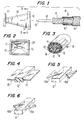
- Fig. 1 shows a dielectric waveguide 10, according to the invention, having a core 12 with a tapered end 13, a cladding 14 surrounding the core 12, an electromagnetic shielding layer 16 surrounding the cladding, and an external absorber 18 surrounding the layer 16.
- a launcher 20 with conventional flange 21 is connected to the dielectric waveguide 10, electromagnetic energy enters the launcher 20.
- An impedance transformation is carried out in the taper 13 of the core 12 of waveguide 10 such that the energy is coupled efficiently into the core 12 of dielectric waveguide 10. Once captured by the core 12, propagation takes place through the core 12 which is surrounded by the cladding 14.
- the core 12 is polytetrafluoroethylene and the cladding 14 is polytetrafluoroethylene, preferably expanded, porous polytetrafluoroethylene tape overwrapped over core 12.
- the cladding layer 14 may be of polytetrafluoroethylene extruded over core 12. Propagation uses the core/cladding interface to harness the energy.
- Mode suppression filters 15 may be secured to the wall of launcher 20.
- the filters 15 are of an electromagnetically lossy material, and are mica cards.
- the electromagnetic shield 16 is provided as well as the external absorber 18.
- the shield is preferably aluminized Kapton (Registered Trade Mark) polyimide tape, and the absorber is preferably carbon-filled PTFE tape.
- the mode suppression filters 15 are secured to the launching horn 20 such that, upon insertion of the waveguide 10 into the horn 20, the filters 15 may or may not penetrate and become embedded within the cladding 14.
- Fig. 4 shows a core 12 with mode suppression filters 15 located adjacent thereto.
- the cladding and outer coverings are omitted for clarity of illustration.
- Fig. 5 shows an alternative embodiment of core 12 having triangular shaped mode suppression filters 15A positioned adjacent thereto.
- Fig. 6 shows a further alternative embodiment of core 12 having triangular shaped mode suppression filters 15B positioned adjacent thereto in an inverted configuration from that of Fig. 5.
- the cladding and outer coverings are omitted from Figs. 5 and 6 for clarity of illustration.
Landscapes
- Control Of Motors That Do Not Use Commutators (AREA)
- Waveguides (AREA)
- Organic Insulating Materials (AREA)
- Developing Agents For Electrophotography (AREA)
- Glass Compositions (AREA)
- Photoreceptors In Electrophotography (AREA)
- Inorganic Insulating Materials (AREA)
- Optical Fibers, Optical Fiber Cores, And Optical Fiber Bundles (AREA)
- Light Guides In General And Applications Therefor (AREA)
- Absorbent Articles And Supports Therefor (AREA)
- Confectionery (AREA)
- Removal Of Floating Material (AREA)
- Laminated Bodies (AREA)
- Shielding Devices Or Components To Electric Or Magnetic Fields (AREA)
Abstract
Description
- This invention relates to a dielectric waveguide for the transmission of electromagnetic waves. More particularly, the invention relates to a dielectric waveguide having higher order mode suppression filters.
- Electromagnetic fields are characterised by the presence of an electric field vector E orthogonal to a magnetic field vector H. The oscillation of these components produce a resultant wave which travels in free space at the velocity of light and is transverse to both of these vectors. The power magnitude and direction of this wave is obtained from the Poynting vector given by:

Electromagnetic waves may exist in both unbounded media (free space) and bounded media (such as coaxial cables and waveguides). This invention is concerned with the behaviour of electromagnetic energy in a bounded medium and, in particular, in a dielectric waveguide. - For propagation of electromagnetic energy to take place in a bounded medium, it is necessary that Maxwell's equations are satisfied when the appropriate boundary conditions are employed.
- In a conventional metal waveguide, these conditions are that the tangential component of the electric field, Et, is zero at the metal boundary and also that the normal component of the magnetic flux density, Bn, is zero.
- The behaviour of such a waveguide structure is well understood. Under excitation from external frequency sources, characteristic field distributions or modes will be set-up. These modes can be controlled by variation of frequency, waveguide shape and/or size. For regular shapes, such as rectangles, squares or circles, the well-defined boundary conditions mean that operation over a specific frequency band using a specific mode is guaranteed. This is the case with most rectangular waveguide systems operating in a pure TE₁₀ mode. This is known as the dominant mode in that it is the first mode to be encountered as the frequency is increased. The TEmn type nomenclature designates the number of half sinusoidal field variations along the x and y axes, respectively.
- Another family of modes in standard rectangular waveguides are the TMmn modes, which are treated in the same way. They are differentiated by the fact that TEmn modes have no Ez component, while TMmn modes have no Hz component.
- The dielectric waveguide disclosed in U.S. Patent 4,463,329 does not have such well-defined boundary conditions. In such a dielectric waveguide, fields will exist in the polytetrafluoroethylene (PTFE) cladding medium. Their magnitude will decay exponentially as a function of distance away from the core medium. This phenomenon also means that, unlike conventional waveguides, numerous modes may, to some degree, be supported in the waveguide depending upon the difference in dielectric constant between the mediums, the frequency of operation and the physical dimensions involved. The presence of these so-called "higher order" modes is undesirable in that they extract energy away from the dominant mode, causing excess loss. They cause, in certain cases, severe amplitude ripple and they contribute to poor phase stability under conditions of flexure.
- US patent 4,344,053 discloses the use of mode suppressor resistance cards located across a conventional waveguide. However, the disclosure is limited to a consideration of hollow waveguides.
- A launching horn employed in conjunction with a waveguide taper performs a complex transformation from conventional waveguide to the dielectric waveguide.
- Techniques such as the finite element method may be used to make this transformation as efficient as possible. However, the presence of any impedance discontinuity will result in the excitation of higher order modes.
- According to the present invention there is provided a dielectric waveguide for the transmission of electromagnetic waves comprising a core of PTFE, one or more layers of PTFE cladding overwrapped around said core; mode suppression filters of an electromagnetically lossy material embedded in said waveguide, said mode suppression filters being mica cards embedded in said cladding; and an electromagnetic shielding layer covering said cladding.
- The mode suppression filters may be affixed to a launcher. The core may be extruded, unsintered PTFE; extruded, sintered PTFE; expanded, unsintered, porous PTFE; or expanded, sintered, porous PTFE. The core may contain a filler. The or each cladding layer may be extruded, unsintered PTFE; extruded, sintered PTFE; expanded, unsintered, porous PTFE; or expanded, sintered, porous PTFE. The cladding layer may contain a filler. The electromagnetic shielding layer covering the cladding preferably is aluminized tape, and most preferably is aluminized Kapton (Registered Trade Mark) polyimide tape. The dielectric waveguide may be further overwrapped with a tape of carbon-filled PTFE.
- A dielectric waveguide emobdying the invention and incorporating mode suppression filters will now be described, by way of example, with reference to the accompanying drawings in which:-
- Fig. 1 is a side elevation of the waveguide, with parts of the waveguide cut away for illustration purposes, and also showing one launcher;
- Fig. 2 is an elevational view, partly in cross section, of the launcher taken along line 2-2 of Fig. 1;
- Fig. 3 is a perspective view, partly in cross section, of the waveguide and mode suppression filters; and
- Figs. 4, 5 and 6 are perspective views of modified waveguide core and mode suppression filters with the cladding and outer layers omitted for clarity of illustration.
- The dielectric waveguide for the transmission of electromagnetic waves comprises a core of polytetrafluoroethylene (PTFE), one or more layers of PTFE cladding overwrapped around the core, the cladding having mode suppression filters of an electromagnetically lossy material embedded therein, and an electromagnetic shielding layer covering the cladding. The mode suppression filters are preferably mica cards.
- The composition of the higher order modes which are created and supported in the dielectric waveguide assembly have field distributions which are unique from the desired, fundamental mode of propagation. Subsequently, it is possible to filter out these unwanted modes by consideration and placement in the waveguide of resistive cards such as mica. Placement of the mica cards should be such that there is little or no interruption of the desired mode.
- Because the desired mode is vertically polarized, it has no component in the same plane as the filters. However, the presence of TEmn and TMmn modes, where n ≠ O, would mean that the filtering action would start to take place on these modes, thus leading to their attenuation. Depending upon the desired effect, these cards can be oriented as desired. They may be of arbitrary shape, but are preferably of the shapes shown in the drawings described below. These shapes ensure that there is a smooth transition into the launcher rather than an abrupt discontinuity, which would mean that the incident energy would be reflected rather than absorbed.
- The filters may be inserted into the cladding by slitting the cladding and fitting them in place. Another method is to cast or secure them in the launching horn.
- In the drawings, Fig. 1 shows a
dielectric waveguide 10, according to the invention, having acore 12 with atapered end 13, acladding 14 surrounding thecore 12, anelectromagnetic shielding layer 16 surrounding the cladding, and anexternal absorber 18 surrounding thelayer 16. When alauncher 20 withconventional flange 21, is connected to thedielectric waveguide 10, electromagnetic energy enters thelauncher 20. An impedance transformation is carried out in thetaper 13 of thecore 12 ofwaveguide 10 such that the energy is coupled efficiently into thecore 12 ofdielectric waveguide 10. Once captured by thecore 12, propagation takes place through thecore 12 which is surrounded by thecladding 14. Thecore 12 is polytetrafluoroethylene and thecladding 14 is polytetrafluoroethylene, preferably expanded, porous polytetrafluoroethylene tape overwrapped overcore 12. Thecladding layer 14 may be of polytetrafluoroethylene extruded overcore 12. Propagation uses the core/cladding interface to harness the energy.Mode suppression filters 15 may be secured to the wall oflauncher 20. Thefilters 15 are of an electromagnetically lossy material, and are mica cards. - To prevent cross-coupling or interference from external sources, the
electromagnetic shield 16 is provided as well as theexternal absorber 18. The shield is preferably aluminized Kapton (Registered Trade Mark) polyimide tape, and the absorber is preferably carbon-filled PTFE tape. - Within the
opening 17 oflauncher 20, shown in Fig. 2, the mode suppression filters 15 are secured to the launchinghorn 20 such that, upon insertion of thewaveguide 10 into thehorn 20, thefilters 15 may or may not penetrate and become embedded within thecladding 14. - In the embodiment of Fig. 3,
rectangular mica cards 15 are inserted into slits in thecladding 14 and are oriented in the horizontal plane as shown adjacent thecore 12. - Fig. 4 shows a core 12 with mode suppression filters 15 located adjacent thereto. The cladding and outer coverings are omitted for clarity of illustration.
- Fig. 5 shows an alternative embodiment of
core 12 having triangular shapedmode suppression filters 15A positioned adjacent thereto. - Fig. 6 shows a further alternative embodiment of
core 12 having triangular shaped mode suppression filters 15B positioned adjacent thereto in an inverted configuration from that of Fig. 5. The cladding and outer coverings are omitted from Figs. 5 and 6 for clarity of illustration.
Claims (7)
- A dielectric waveguide for the transmission of electromagnetic waves, characterised by a core (12) of PTFE, one or more layers of PTFE cladding (14) overwrapped around said core; mode suppression filters (15) of an electromagnetically lossy material embedded in said waveguide, said mode suppression filters being mica cards embedded in said cladding; and an electromagnetic shielding layer (16) covering said cladding.
- A dielectric waveguide according to claim 1, characterised in that said core is extruded, unsintered PTFE; extruded sintered PTFE; expanded, unsintered, porous PTFE, or expanded sintered PTFE.
- A dielectric waveguide according to claim 1, characterised in that said core and/or said cladding contains a filler.
- A dielectric waveguide according to claim 1, characterised in that the or each said cladding layer is extruded, unsintered PTFE; extruded sintered PTFE; expanded unsintered porous PTFE or expanded sintered porous PTFE.
- A dielectric waveguide according to claim 1, characterised in that said shielding layer is aluminized tape.
- A dielectric waveguide according to claim 5 characterised in that it is overwrapped with a tape of carbon-filled PTFE.
- A dielectric waveguide according to claim 1, characterised in that it is used in association with a launching horn, wherein said mode suppression filters are secured to said launching horn.
Priority Applications (1)
| Application Number | Priority Date | Filing Date | Title |
|---|---|---|---|
| AT88307987T ATE97260T1 (en) | 1987-09-29 | 1988-08-30 | DIELECTRIC WAVE GUIDE. |
Applications Claiming Priority (2)
| Application Number | Priority Date | Filing Date | Title |
|---|---|---|---|
| US07/101,987 US4792774A (en) | 1987-09-29 | 1987-09-29 | Dielectric waveguide having higher order mode suppression filters |
| US101987 | 1987-09-29 |
Publications (3)
| Publication Number | Publication Date |
|---|---|
| EP0310243A2 EP0310243A2 (en) | 1989-04-05 |
| EP0310243A3 EP0310243A3 (en) | 1989-05-24 |
| EP0310243B1 true EP0310243B1 (en) | 1993-11-10 |
Family
ID=22287523
Family Applications (1)
| Application Number | Title | Priority Date | Filing Date |
|---|---|---|---|
| EP88307987A Expired - Lifetime EP0310243B1 (en) | 1987-09-29 | 1988-08-30 | A dielectric waveguide |
Country Status (13)
| Country | Link |
|---|---|
| US (1) | US4792774A (en) |
| EP (1) | EP0310243B1 (en) |
| JP (1) | JPH0289402A (en) |
| AT (1) | ATE97260T1 (en) |
| AU (1) | AU600633B2 (en) |
| DE (1) | DE3885566T2 (en) |
| DK (1) | DK537488A (en) |
| FI (1) | FI884237L (en) |
| GB (1) | GB2210732B (en) |
| HK (1) | HK122293A (en) |
| IL (1) | IL87541A0 (en) |
| NO (1) | NO884059L (en) |
| PT (1) | PT88593A (en) |
Families Citing this family (6)
| Publication number | Priority date | Publication date | Assignee | Title |
|---|---|---|---|---|
| US5325457A (en) * | 1991-09-20 | 1994-06-28 | Bottoms Jack Jr | Field protected self-supporting fiber optic cable |
| US6229939B1 (en) * | 1999-06-03 | 2001-05-08 | Trw Inc. | High power fiber ribbon laser and amplifier |
| US10199706B2 (en) | 2016-10-21 | 2019-02-05 | International Business Machines Corporation | Communication system having a multi-layer PCB including a dielectric waveguide layer with a core and cladding directly contacting ground planes |
| US10978773B2 (en) * | 2018-12-03 | 2021-04-13 | At&T Intellectual Property I, L.P. | Guided wave dielectric coupler having a dielectric cable with an exposed dielectric core position for enabling electromagnetic coupling between the cable and a transmission medium |
| EP3995836B1 (en) * | 2020-11-05 | 2024-05-15 | Universidad Carlos III de Madrid | Ultra-wideband interconnection |
| JP2024141455A (en) * | 2023-03-29 | 2024-10-10 | 株式会社Nttドコモ | Dielectric Waveguide Connectors |
Family Cites Families (19)
| Publication number | Priority date | Publication date | Assignee | Title |
|---|---|---|---|---|
| DE1047897B (en) * | 1952-04-15 | 1958-12-31 | Siemens Ag | Waveguide arrangement consisting of one or more layers of dielectric material |
| DE1006029B (en) * | 1954-05-24 | 1957-04-11 | Siemens Ag | Dielectric waveguide for the transmission of surface waves |
| US2849692A (en) * | 1954-08-18 | 1958-08-26 | Bell Telephone Labor Inc | Dielectric guide for electromagnetic waves |
| GB1078304A (en) * | 1963-08-06 | 1967-08-09 | Lignes Telegraph Telephon | Improvements in or relating to electromagnetic wave transmission lines |
| FR1372610A (en) * | 1963-08-06 | 1964-09-18 | Transmission line with dielectric | |
| JPS4933187B1 (en) * | 1968-09-27 | 1974-09-05 | ||
| GB1338384A (en) * | 1969-12-17 | 1973-11-21 | Post Office | Dielectric waveguides |
| JPS5535683B2 (en) * | 1973-08-10 | 1980-09-16 | ||
| GB1473655A (en) * | 1974-11-15 | 1977-05-18 | Post Office | Dielectric waveguides |
| JPS5293254A (en) * | 1976-01-31 | 1977-08-05 | Anritsu Electric Co Ltd | Mode converter |
| US4040061A (en) * | 1976-06-01 | 1977-08-02 | Gte Sylvania Incorporated | Broadband corrugated horn antenna |
| JPS5813702B2 (en) * | 1978-03-16 | 1983-03-15 | 利晴 信達 | Striped steel plate non-slip for stairs |
| US4463329A (en) * | 1978-08-15 | 1984-07-31 | Hirosuke Suzuki | Dielectric waveguide |
| US4344053A (en) * | 1981-02-12 | 1982-08-10 | Litton Systems, Inc. | Mode suppressor for circular waveguides utilizing a plurality of resistance cards |
| JPS58191503A (en) * | 1982-05-01 | 1983-11-08 | Junkosha Co Ltd | Transmission line |
| JPS61163704A (en) * | 1985-01-16 | 1986-07-24 | Junkosha Co Ltd | Dielectric line |
| JPH0667069B2 (en) * | 1986-02-07 | 1994-08-24 | 三菱電機株式会社 | Gas insulated switchgear |
| US4785268A (en) * | 1987-07-30 | 1988-11-15 | W. L Gore & Associates, Inc. | Dielectric waveguide delay line |
| US4875026A (en) * | 1987-08-17 | 1989-10-17 | W. L. Gore & Associates, Inc. | Dielectric waveguide having higher order mode suppression |
-
1987
- 1987-09-29 US US07/101,987 patent/US4792774A/en not_active Expired - Fee Related
-
1988
- 1988-07-08 AU AU18866/88A patent/AU600633B2/en not_active Expired - Fee Related
- 1988-08-23 IL IL8887541A patent/IL87541A0/en unknown
- 1988-08-30 DE DE3885566T patent/DE3885566T2/en not_active Expired - Fee Related
- 1988-08-30 AT AT88307987T patent/ATE97260T1/en not_active IP Right Cessation
- 1988-08-30 GB GB8820516A patent/GB2210732B/en not_active Revoked
- 1988-08-30 EP EP88307987A patent/EP0310243B1/en not_active Expired - Lifetime
- 1988-09-13 NO NO88884059A patent/NO884059L/en unknown
- 1988-09-14 FI FI884237A patent/FI884237L/en not_active IP Right Cessation
- 1988-09-14 JP JP88228870A patent/JPH0289402A/en active Pending
- 1988-09-27 DK DK537488A patent/DK537488A/en not_active Application Discontinuation
- 1988-09-27 PT PT88593A patent/PT88593A/en not_active Application Discontinuation
-
1993
- 1993-11-11 HK HK1222/93A patent/HK122293A/en unknown
Also Published As
| Publication number | Publication date |
|---|---|
| US4792774A (en) | 1988-12-20 |
| AU1886688A (en) | 1989-04-06 |
| FI884237A7 (en) | 1989-03-30 |
| IL87541A0 (en) | 1989-01-31 |
| DK537488D0 (en) | 1988-09-27 |
| EP0310243A3 (en) | 1989-05-24 |
| GB2210732B (en) | 1991-07-24 |
| DK537488A (en) | 1989-03-30 |
| HK122293A (en) | 1993-11-19 |
| AU600633B2 (en) | 1990-08-16 |
| ATE97260T1 (en) | 1993-11-15 |
| NO884059D0 (en) | 1988-09-13 |
| NO884059L (en) | 1989-03-30 |
| DE3885566D1 (en) | 1993-12-16 |
| EP0310243A2 (en) | 1989-04-05 |
| FI884237A0 (en) | 1988-09-14 |
| FI884237L (en) | 1989-03-30 |
| JPH0289402A (en) | 1990-03-29 |
| PT88593A (en) | 1989-07-31 |
| DE3885566T2 (en) | 1994-05-26 |
| GB8820516D0 (en) | 1988-09-28 |
| GB2210732A (en) | 1989-06-14 |
Similar Documents
| Publication | Publication Date | Title |
|---|---|---|
| EP0304141B1 (en) | A dielectric waveguide | |
| US3845426A (en) | Dipole mode electromagnetic waveguides | |
| US3219954A (en) | Surface wave transmission system for telecommunication and power transmission | |
| US4392039A (en) | Dielectric heating applicator | |
| US10615474B2 (en) | Apparatuses and methods for mode suppression in rectangular waveguide | |
| US4238747A (en) | Mode filter apparatus | |
| EP0310243A2 (en) | A dielectric waveguide | |
| EP0301674B1 (en) | A dielectric delay line | |
| EP0318198A1 (en) | A dielectric waveguide | |
| CA1258892A (en) | Attenuation and time delay equalizer for a waveguide filter | |
| US3184695A (en) | Circular electric mode filter | |
| US2534876A (en) | Wave guide coupling arrangement | |
| US3078428A (en) | Spurious mode suppressing wave guide | |
| EP0360415B1 (en) | Dielectric waveguide | |
| GB1597673A (en) | Non reciprocal microwave phase shifters operating in a wide band on edge mode | |
| US2940057A (en) | Selective mode filters | |
| Han et al. | Coupling characteristics of eccentric arranged dielectric disk and ring | |
| EP0335570A1 (en) | Transmission Line | |
| Biswas et al. | Propagation along a dielectric‐coated cylinder immersed in a magnetoplasma | |
| RU2065235C1 (en) | Guide antenna with large beam width | |
| Kim et al. | Small‐sized waveguides with periodically loaded double posts | |
| Sipus et al. | Green's functions for strip-loaded grounded dielectric slab derived without using Floquet mode expansion | |
| JPS61208779A (en) | High frequency heater | |
| Unrau | Spurious mode suppression in quasioptical waveguides by lossy dielectric sidewall coatings | |
| Fan et al. | Edge coupled strip inset dielectric guide |
Legal Events
| Date | Code | Title | Description |
|---|---|---|---|
| PUAI | Public reference made under article 153(3) epc to a published international application that has entered the european phase |
Free format text: ORIGINAL CODE: 0009012 |
|
| PUAL | Search report despatched |
Free format text: ORIGINAL CODE: 0009013 |
|
| AK | Designated contracting states |
Kind code of ref document: A2 Designated state(s): AT BE CH DE ES FR GB GR IT LI LU NL SE |
|
| AK | Designated contracting states |
Kind code of ref document: A3 Designated state(s): AT BE CH DE ES FR GB GR IT LI LU NL SE |
|
| 17P | Request for examination filed |
Effective date: 19891009 |
|
| 17Q | First examination report despatched |
Effective date: 19920408 |
|
| GRAA | (expected) grant |
Free format text: ORIGINAL CODE: 0009210 |
|
| AK | Designated contracting states |
Kind code of ref document: B1 Designated state(s): AT BE CH DE ES FR GB GR IT LI LU NL SE |
|
| PG25 | Lapsed in a contracting state [announced via postgrant information from national office to epo] |
Ref country code: NL Effective date: 19931110 Ref country code: LI Effective date: 19931110 Ref country code: GR Free format text: LAPSE BECAUSE OF FAILURE TO SUBMIT A TRANSLATION OF THE DESCRIPTION OR TO PAY THE FEE WITHIN THE PRESCRIBED TIME-LIMIT Effective date: 19931110 Ref country code: ES Free format text: THE PATENT HAS BEEN ANNULLED BY A DECISION OF A NATIONAL AUTHORITY Effective date: 19931110 Ref country code: CH Effective date: 19931110 Ref country code: BE Effective date: 19931110 Ref country code: AT Effective date: 19931110 |
|
| REF | Corresponds to: |
Ref document number: 97260 Country of ref document: AT Date of ref document: 19931115 Kind code of ref document: T |
|
| ITF | It: translation for a ep patent filed | ||
| REF | Corresponds to: |
Ref document number: 3885566 Country of ref document: DE Date of ref document: 19931216 |
|
| ET | Fr: translation filed | ||
| REG | Reference to a national code |
Ref country code: CH Ref legal event code: PL |
|
| NLV1 | Nl: lapsed or annulled due to failure to fulfill the requirements of art. 29p and 29m of the patents act | ||
| PGFP | Annual fee paid to national office [announced via postgrant information from national office to epo] |
Ref country code: FR Payment date: 19940712 Year of fee payment: 7 |
|
| PGFP | Annual fee paid to national office [announced via postgrant information from national office to epo] |
Ref country code: DE Payment date: 19940725 Year of fee payment: 7 |
|
| PGFP | Annual fee paid to national office [announced via postgrant information from national office to epo] |
Ref country code: GB Payment date: 19940728 Year of fee payment: 7 |
|
| PG25 | Lapsed in a contracting state [announced via postgrant information from national office to epo] |
Ref country code: LU Free format text: LAPSE BECAUSE OF NON-PAYMENT OF DUE FEES Effective date: 19940831 |
|
| PGFP | Annual fee paid to national office [announced via postgrant information from national office to epo] |
Ref country code: SE Payment date: 19940831 Year of fee payment: 7 |
|
| PLBE | No opposition filed within time limit |
Free format text: ORIGINAL CODE: 0009261 |
|
| STAA | Information on the status of an ep patent application or granted ep patent |
Free format text: STATUS: NO OPPOSITION FILED WITHIN TIME LIMIT |
|
| 26N | No opposition filed | ||
| EAL | Se: european patent in force in sweden |
Ref document number: 88307987.3 |
|
| PG25 | Lapsed in a contracting state [announced via postgrant information from national office to epo] |
Ref country code: GB Effective date: 19950830 |
|
| PG25 | Lapsed in a contracting state [announced via postgrant information from national office to epo] |
Ref country code: SE Effective date: 19950831 |
|
| PG25 | Lapsed in a contracting state [announced via postgrant information from national office to epo] |
Ref country code: FR Effective date: 19960430 |
|
| GBPC | Gb: european patent ceased through non-payment of renewal fee |
Effective date: 19950830 |
|
| PG25 | Lapsed in a contracting state [announced via postgrant information from national office to epo] |
Ref country code: DE Effective date: 19960501 |
|
| EUG | Se: european patent has lapsed |
Ref document number: 88307987.3 |
|
| REG | Reference to a national code |
Ref country code: FR Ref legal event code: ST |
|
| PG25 | Lapsed in a contracting state [announced via postgrant information from national office to epo] |
Ref country code: IT Free format text: LAPSE BECAUSE OF NON-PAYMENT OF DUE FEES;WARNING: LAPSES OF ITALIAN PATENTS WITH EFFECTIVE DATE BEFORE 2007 MAY HAVE OCCURRED AT ANY TIME BEFORE 2007. THE CORRECT EFFECTIVE DATE MAY BE DIFFERENT FROM THE ONE RECORDED. Effective date: 20050830 |
|
| PGFP | Annual fee paid to national office [announced via postgrant information from national office to epo] |
Ref country code: IT Payment date: 20070622 Year of fee payment: 20 |
|
| PGRI | Patent reinstated in contracting state [announced from national office to epo] |
Ref country code: IT Effective date: 20091201 |