EP0310047A2 - Double-diffused mos fet - Google Patents
Double-diffused mos fet Download PDFInfo
- Publication number
- EP0310047A2 EP0310047A2 EP88116031A EP88116031A EP0310047A2 EP 0310047 A2 EP0310047 A2 EP 0310047A2 EP 88116031 A EP88116031 A EP 88116031A EP 88116031 A EP88116031 A EP 88116031A EP 0310047 A2 EP0310047 A2 EP 0310047A2
- Authority
- EP
- European Patent Office
- Prior art keywords
- semiconductor regions
- regions
- semiconductor
- region
- periphery
- Prior art date
- Legal status (The legal status is an assumption and is not a legal conclusion. Google has not performed a legal analysis and makes no representation as to the accuracy of the status listed.)
- Withdrawn
Links
- 239000004065 semiconductor Substances 0.000 claims abstract description 46
- 239000000758 substrate Substances 0.000 claims abstract description 11
- 239000012535 impurity Substances 0.000 claims description 10
- 229910021420 polycrystalline silicon Inorganic materials 0.000 claims description 2
- 229920005591 polysilicon Polymers 0.000 claims description 2
- 108091006146 Channels Proteins 0.000 abstract description 28
- 230000003071 parasitic effect Effects 0.000 abstract description 15
- 108010075750 P-Type Calcium Channels Proteins 0.000 abstract description 4
- 239000010410 layer Substances 0.000 description 22
- 230000000875 corresponding effect Effects 0.000 description 8
- 238000009792 diffusion process Methods 0.000 description 6
- XUIMIQQOPSSXEZ-UHFFFAOYSA-N Silicon Chemical compound [Si] XUIMIQQOPSSXEZ-UHFFFAOYSA-N 0.000 description 4
- 229910052710 silicon Inorganic materials 0.000 description 4
- 239000010703 silicon Substances 0.000 description 4
- 230000001939 inductive effect Effects 0.000 description 3
- ZOXJGFHDIHLPTG-UHFFFAOYSA-N Boron Chemical compound [B] ZOXJGFHDIHLPTG-UHFFFAOYSA-N 0.000 description 2
- VYPSYNLAJGMNEJ-UHFFFAOYSA-N Silicium dioxide Chemical compound O=[Si]=O VYPSYNLAJGMNEJ-UHFFFAOYSA-N 0.000 description 2
- XAGFODPZIPBFFR-UHFFFAOYSA-N aluminium Chemical compound [Al] XAGFODPZIPBFFR-UHFFFAOYSA-N 0.000 description 2
- 229910052782 aluminium Inorganic materials 0.000 description 2
- 229910052796 boron Inorganic materials 0.000 description 2
- 230000006378 damage Effects 0.000 description 2
- 229910052814 silicon oxide Inorganic materials 0.000 description 2
- 238000009751 slip forming Methods 0.000 description 2
- OAICVXFJPJFONN-UHFFFAOYSA-N Phosphorus Chemical compound [P] OAICVXFJPJFONN-UHFFFAOYSA-N 0.000 description 1
- 229910052581 Si3N4 Inorganic materials 0.000 description 1
- 229910052787 antimony Inorganic materials 0.000 description 1
- WATWJIUSRGPENY-UHFFFAOYSA-N antimony atom Chemical compound [Sb] WATWJIUSRGPENY-UHFFFAOYSA-N 0.000 description 1
- 229910052785 arsenic Inorganic materials 0.000 description 1
- RQNWIZPPADIBDY-UHFFFAOYSA-N arsenic atom Chemical compound [As] RQNWIZPPADIBDY-UHFFFAOYSA-N 0.000 description 1
- 230000003247 decreasing effect Effects 0.000 description 1
- 239000011229 interlayer Substances 0.000 description 1
- 238000004519 manufacturing process Methods 0.000 description 1
- 229910052698 phosphorus Inorganic materials 0.000 description 1
- 239000011574 phosphorus Substances 0.000 description 1
- 239000011241 protective layer Substances 0.000 description 1
- HQVNEWCFYHHQES-UHFFFAOYSA-N silicon nitride Chemical compound N12[Si]34N5[Si]62N3[Si]51N64 HQVNEWCFYHHQES-UHFFFAOYSA-N 0.000 description 1
Images


Classifications
-
- H—ELECTRICITY
- H01—ELECTRIC ELEMENTS
- H01L—SEMICONDUCTOR DEVICES NOT COVERED BY CLASS H10
- H01L29/00—Semiconductor devices adapted for rectifying, amplifying, oscillating or switching, or capacitors or resistors with at least one potential-jump barrier or surface barrier, e.g. PN junction depletion layer or carrier concentration layer; Details of semiconductor bodies or of electrodes thereof ; Multistep manufacturing processes therefor
- H01L29/66—Types of semiconductor device ; Multistep manufacturing processes therefor
- H01L29/68—Types of semiconductor device ; Multistep manufacturing processes therefor controllable by only the electric current supplied, or only the electric potential applied, to an electrode which does not carry the current to be rectified, amplified or switched
- H01L29/76—Unipolar devices, e.g. field effect transistors
- H01L29/772—Field effect transistors
- H01L29/78—Field effect transistors with field effect produced by an insulated gate
- H01L29/7801—DMOS transistors, i.e. MISFETs with a channel accommodating body or base region adjoining a drain drift region
- H01L29/7802—Vertical DMOS transistors, i.e. VDMOS transistors
-
- H—ELECTRICITY
- H01—ELECTRIC ELEMENTS
- H01L—SEMICONDUCTOR DEVICES NOT COVERED BY CLASS H10
- H01L29/00—Semiconductor devices adapted for rectifying, amplifying, oscillating or switching, or capacitors or resistors with at least one potential-jump barrier or surface barrier, e.g. PN junction depletion layer or carrier concentration layer; Details of semiconductor bodies or of electrodes thereof ; Multistep manufacturing processes therefor
- H01L29/02—Semiconductor bodies ; Multistep manufacturing processes therefor
- H01L29/06—Semiconductor bodies ; Multistep manufacturing processes therefor characterised by their shape; characterised by the shapes, relative sizes, or dispositions of the semiconductor regions ; characterised by the concentration or distribution of impurities within semiconductor regions
- H01L29/0684—Semiconductor bodies ; Multistep manufacturing processes therefor characterised by their shape; characterised by the shapes, relative sizes, or dispositions of the semiconductor regions ; characterised by the concentration or distribution of impurities within semiconductor regions characterised by the shape, relative sizes or dispositions of the semiconductor regions or junctions between the regions
- H01L29/0692—Surface layout
- H01L29/0696—Surface layout of cellular field-effect devices, e.g. multicellular DMOS transistors or IGBTs
-
- H—ELECTRICITY
- H01—ELECTRIC ELEMENTS
- H01L—SEMICONDUCTOR DEVICES NOT COVERED BY CLASS H10
- H01L29/00—Semiconductor devices adapted for rectifying, amplifying, oscillating or switching, or capacitors or resistors with at least one potential-jump barrier or surface barrier, e.g. PN junction depletion layer or carrier concentration layer; Details of semiconductor bodies or of electrodes thereof ; Multistep manufacturing processes therefor
- H01L29/40—Electrodes ; Multistep manufacturing processes therefor
- H01L29/41—Electrodes ; Multistep manufacturing processes therefor characterised by their shape, relative sizes or dispositions
- H01L29/423—Electrodes ; Multistep manufacturing processes therefor characterised by their shape, relative sizes or dispositions not carrying the current to be rectified, amplified or switched
- H01L29/42312—Gate electrodes for field effect devices
- H01L29/42316—Gate electrodes for field effect devices for field-effect transistors
- H01L29/4232—Gate electrodes for field effect devices for field-effect transistors with insulated gate
- H01L29/42372—Gate electrodes for field effect devices for field-effect transistors with insulated gate characterised by the conducting layer, e.g. the length, the sectional shape or the lay-out
- H01L29/4238—Gate electrodes for field effect devices for field-effect transistors with insulated gate characterised by the conducting layer, e.g. the length, the sectional shape or the lay-out characterised by the surface lay-out
Definitions
- the present invention relates to a double-diffused MOS FET used mainly for power control.
- a double-diffused MOS FET is generally used for power control, and is constituted by a plurality of unit FET cells connected in parallel.
- Fig. 1 is a plan view showing an arrangement of a conventional D-MOS comprising unit FET cells each having a square top surface
- Fig. 2 is a sectional view taken along line A - A′ of Fig. 1.
- low-concentration n-type epitaxial layer 11 is deposited on a surface of high-concentration n-type silicon substrate 10.
- Substrate 10 and epitaxial layer 11 together constitute a drain region of each unit FET cell.
- P+-type low-resistance regions 12 are formed separately at a plurality of positions on the surface of epitaxial layer 11, and p-type channel base regions 13 are respectively formed around regions 12.
- N+-type source region 14 is continuously formed on the surfaces of each low-resistance region 12 and each channel base region 13.
- a gate electrode 16 is formed on the surface of each channel base region 13, through gate insulating layer 15, and is patterned in the form of a mesh constituted by a plurality of square openings 17.
- reference numeral 18 denotes a source electrode which is connected to each of low-resistance regions 12 and source regions 14, and which is common to all the unit FET cells.
- drain electrode 19 is connected to the other surface of substrate 10.
- npn bipolar transistor Q constituted by n-type epitaxial region 11 as a collector, p-type channel base region 12 as a base, and source region 14 as an emitter is parasitically generated. Furthermore, parasitic resistance Rb due to a diffusion resistance in low-concentration channel base region 13 is formed between the base and emitter of transistor Q.
- low-resistance region 12 and channel base region 13 are respectively formed into square patterns. Being formed in this manner, the distance between the peripheries of region 12 and channel base region 13 which is located outward therefrom, is quite large at the respective corners of the unit FET cell. As a result, the value of parasitic resistance Rb varies depending on positions in the unit FET cell. For example, the distance from the periphery of low-resistance region 12 to that of channel base region 13, located outward therefrom, becomes relatively small at a position along line a - a′ in Fig. 4. For this reason, the value of parasitic resistance Rb at this position becomes relatively small.
- the present invention has been developed in consideration of the above situation, and has as its object to provide a double-diffused MOS FET has good resistance to destruction caused when a parasitic bipolar transistor is rendered conductive.
- a double-diffused MOS FET comprising a semiconductor substrate having parallel first and second planar surfaces and doped with an impurity of a first conductivity type, a plurality of first semiconductor regions of a second conductivity type, diffused in the form of a mesh in the first planar surface of the substrate, each of the first semiconductor regions having a substantially square periphery with four rounded corners, a plurality of second semiconductor regions of the second conductivity type, each of which is diffused so as to surround a corresponding one of the first semiconductor regions, has a depth less than that of the first semiconductor region, and has a periphery the shape of which corresponds to that of the first semiconductor region, the planar distance from the periphery of each of the first second semiconductor regions to that of a corresponding one of the first semiconductor regions being set to be equal throughout the periphery of each of the first semiconductor regions, a plurality of source regions
- Reference numeral 20 denotes a silicon semiconductor layer.
- Antimony or arsenic is doped as an n-type impurity in semiconductor layer 20, at a concentration of, for example, about 1 x 10¹⁸ to 1 x 10²⁰ (/cm3).
- Semiconductor layer 20 and epitaxial layer 21 constitute n-type substrate 22.
- Semiconductor layer 20 and epitaxial layer 21 serve as a drain for a plurality of unit FETs to be described later.
- P+-type low-resistance regions 23 are formed separately in a plurality of portions of the exposed surface of n-type epitaxial layer 21, and are doped with boron, as a p-type impurity, is doped at a surface concentration of about 1 x 10²⁰ (/cm3).
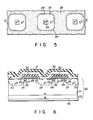
- Low-resistance regions 23 are formed on the exposed surface of n-type epitaxial layer 21 in the form of a mesh, as shown in Fig. 5.
- P-type channel base regions 24 each having a depth less than that of each low-resistance region 23 are respectively formed around low-resistance regions 23. Boron as a p-type impurity is doped in each channel base region 24 at a surface concentration of about 1 .
- a plurality of n-type source regions 25 each having a depth smaller than that of each channel base region 24 are continuously formed on the surfaces of low-resistance regions 23 and channel base regions 24, respectively.
- Each source region 25 is formed such that its periphery is located inward from that of a corresponding channel base region 24 while a predetermined distance is kept between these peripheries.
- Surface region 26 of channel base region 24, which is present between the peripheries of each source region 25 and corresponding channel base region 24, is defined as a channel region of each unit FET cell. Therefore, channel regions 26 of the unit FET cells are formed so as to surround corresponding channel base regions 24.
- Gate insulating layer 27 consisting of silicon oxide is deposited in the form of a mesh so as to surround channel base regions 24 and low-resistance regions 23 and cover channel regions 26 described above.
- gate electrode 28 consisting of polysilicon and having the same shape as that of gate insulating layer 27 is deposited on gate insulating layer 27. As shown in Fig. 5, gate insulating layer 27 and gate electrode 28 formed into the same shape are patterned in the form of a mesh constituted by a plurality of substantially square openings 29 each having rounded four corners.
- a plurality of unit FET cells each constituted by n-type silicon semiconductor and n-type epitaxial layers 20 and 21 as a drain, channel base region 24 as a base, and source region 25 as a source are formed near openings 29.
- Insulating interlayer 30 is deposited on gate electrode 28.
- Source electrode 31 consisting of aluminum is integrally formed on the exposed surfaces of low-resistance regions 23 and source regions 25, so that all source regions 25 are connected to source electrode 31.
- surface protective layer 32 consisting of silicon oxide or silicon nitride is deposited on source electrode 31 by CVD.
- Drain electrode 33 consisting of aluminum is formed on the exposed surface of n-type silicon semiconductor layer 20. Note that each low-resistance region 23 is formed so as to decrease the value of parasitic resistance Rb due to a diffusion resistance between the base and the emitter of parasitic bipolar transistor Q.
- Channel base region 24 is formed by p-type impurity diffusion using gate electrode 28 as a mask. Furthermore, low-resistance region 23 is formed into a shape similar to opening 29. Low-resistance regions 23 are formed by p-type impurity diffusion using a mask (not shown) for impurity diffusion, which has a plurality of openings smaller than openings 29. Then, the mask which is used for forming low-resistance regions 23 is removed.
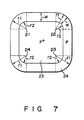
- Fig. 7 is a plan view showing a pattern of channel base region 24 and low-resistance region 23 of one unit FET in the D-MOS of the above embodiment.
- the peripheries of low-resistance region 23 and channel base region 24 are formed into substantially square shapes similar to each other.
- the four corners of regions 23 and 24 respectively constitute parts of concentrical circles respectively defined by radii r1 and r2, and points p1, p2, p3, and p4 as the centers.
- Distance W from the periphery of low-resistance region 23 to that of channel base region 24 is set to be constant at any positions.
- the value of parasitic resistance Rb between the base and the emitter of the bipolar transistor corresponding to parasitic bipolar transistor Q shown in Fig. 3 is set to be constant at any positions in each unit FET.
- the parasitic transistors are turned on in the same manner at any positions in each unit FET, thus solving the problem that only some of the transistors are easily rendered conductive as in the conventional D-MOS.
- the D-MOS of this embodiment has good resistance to destruction caused when an inductive load is driven.
- the D-MOS of this embodiment can be manufactured by only changing the shape of mask pattern for diffusion without specifically adding complex manufacturing processes.
Abstract
Description
- The present invention relates to a double-diffused MOS FET used mainly for power control.
- A double-diffused MOS FET (D-MOS) is generally used for power control, and is constituted by a plurality of unit FET cells connected in parallel. Fig. 1 is a plan view showing an arrangement of a conventional D-MOS comprising unit FET cells each having a square top surface, and Fig. 2 is a sectional view taken along line A - A′ of Fig. 1.
- Referring to Fig. 1, low-concentration n-type epitaxial layer 11 is deposited on a surface of high-concentration n-type silicon substrate 10. Substrate 10 and epitaxial layer 11 together constitute a drain region of each unit FET cell. P⁺-type low-
resistance regions 12 are formed separately at a plurality of positions on the surface of epitaxial layer 11, and p-typechannel base regions 13 are respectively formed aroundregions 12. N⁺-type source region 14 is continuously formed on the surfaces of each low-resistance region 12 and eachchannel base region 13. Agate electrode 16 is formed on the surface of eachchannel base region 13, throughgate insulating layer 15, and is patterned in the form of a mesh constituted by a plurality ofsquare openings 17. The respective unit FET cells are formed nearcorresponding openings 17. Note thatreference numeral 18 denotes a source electrode which is connected to each of low-resistance regions 12 andsource regions 14, and which is common to all the unit FET cells. In addition,drain electrode 19 is connected to the other surface of substrate 10. - In the D-MOS having such an arrangement, as shown in the sectional view of Fig. 3, npn bipolar transistor Q constituted by n-type epitaxial region 11 as a collector, p-type
channel base region 12 as a base, andsource region 14 as an emitter is parasitically generated. Furthermore, parasitic resistance Rb due to a diffusion resistance in low-concentrationchannel base region 13 is formed between the base and emitter of transistor Q. - When a D-MOS is used to control an inductive load, a high voltage is generated upon switching of the D-MOS and causes the above-described parasitic transistor Q to be partially operated, with the result that a large current flows between the source and the drain. As a result, the D-MOS may be destroyed. For this reason, in the conventional D-MOS, the value of resistance Rb is decreased by forming above low-
resistance region 12 so that parasitic transistor Q cannot be easily rendered conductive. - However, as is shown in the plan view of Fig. 4, low-
resistance region 12 andchannel base region 13 are respectively formed into square patterns. Being formed in this manner, the distance between the peripheries ofregion 12 andchannel base region 13 which is located outward therefrom, is quite large at the respective corners of the unit FET cell. As a result, the value of parasitic resistance Rb varies depending on positions in the unit FET cell. For example, the distance from the periphery of low-resistance region 12 to that ofchannel base region 13, located outward therefrom, becomes relatively small at a position along line a - a′ in Fig. 4. For this reason, the value of parasitic resistance Rb at this position becomes relatively small. In contrast to this, the distance from the periphery of low-resistance region 12 to that ofchannel base region 13 located outward therefrom becomes relatively large at a position along line b - b′ in Fig. 4. For this reason, the value of parasitic resistance Rb at a position along line b - b′ is increased with an increase in distance acrosschannel base region 13. - In the conventional D-MOS, parasitic bipolar transistors which are easily turned on at the corners of each unit FET. Therefore, when an inductive load is to be driven, whether the D-MOS itself is destroyed or not is determined by the parasitic bipolar transistors which are generated at the corners and easily turned on.
- The present invention has been developed in consideration of the above situation, and has as its object to provide a double-diffused MOS FET has good resistance to destruction caused when a parasitic bipolar transistor is rendered conductive.
- According to the present invention, there is provided a double-diffused MOS FET comprising a semiconductor substrate having parallel first and second planar surfaces and doped with an impurity of a first conductivity type, a plurality of first semiconductor regions of a second conductivity type, diffused in the form of a mesh in the first planar surface of the substrate, each of the first semiconductor regions having a substantially square periphery with four rounded corners, a plurality of second semiconductor regions of the second conductivity type, each of which is diffused so as to surround a corresponding one of the first semiconductor regions, has a depth less than that of the first semiconductor region, and has a periphery the shape of which corresponds to that of the first semiconductor region, the planar distance from the periphery of each of the first second semiconductor regions to that of a corresponding one of the first semiconductor regions being set to be equal throughout the periphery of each of the first semiconductor regions, a plurality of source regions of the first conductivity type, which are diffused in the plurality of first and second semiconductor regions on the first planar surface and are shallower than the first and second semiconductor regions, the periphery of each of the source regions being located a predetermined distance inward from that of a corresponding one of the second semiconductor regions, a plurality of channel regions constituted by the second semiconductor regions respectively defined between the peripheries of the source and second semiconductor regions, a gate insulating layer extending in the form of a mesh between the first and second semiconductor regions, so as to surround the first and second semiconductor regions and cover the plurality of channel regions, a gate electrode deposited in the form of a mesh on the gate insulating layer, a common source electrode connected to the plurality of source and first semiconductor regions and extending on the first planar surface, and a drain electrode connected to the second planar surface of the substrate.
- This invention can be more fully understood from the following detailed description when taken in conjunction with the accompanying drawings, in which:
- Fig. 1 is a plan view showing a pattern of a conventional double-diffused MOS FET;
- Fig. 2 is a sectional view taken along line A - A′ of Fig. 1;
- Fig. 3 is a schematic sectional view showing an enlarged portion of the sectional view of Fig. 2;
- Fig. 4 is a partial plan view of the pattern shown in Fig. 1;
- Fig. 5 is a plan view showing a pattern of a MOS FET according to an embodiment of the present invention;
- Fig. 6 is a sectional view taken along line B - B′ of Fig. 5; and
- Fig. 7 is a partial view of the pattern shown in Fig. 5.
- A case wherein the present invention is applied to an n-channel D-MOS will be described below with reference to Figs. 5 and 6.
-
Reference numeral 20 denotes a silicon semiconductor layer. Antimony or arsenic is doped as an n-type impurity insemiconductor layer 20, at a concentration of, for example, about 1 x 10¹⁸ to 1 x 10²⁰ (/cm³). N-typeepitaxial layer 21, which is doped with phosphorus as an n-type impurity at a relatively high concentration, e.g., about 1 x 10¹⁵ (/cm³), is formed on one surface ofsemiconductor layer 20.Semiconductor layer 20 andepitaxial layer 21 constitute n-type substrate 22.Semiconductor layer 20 andepitaxial layer 21 serve as a drain for a plurality of unit FETs to be described later. - P⁺-type low-
resistance regions 23 are formed separately in a plurality of portions of the exposed surface of n-typeepitaxial layer 21, and are doped with boron, as a p-type impurity, is doped at a surface concentration of about 1 x 10²⁰ (/cm³). Low-resistance regions 23 are formed on the exposed surface of n-typeepitaxial layer 21 in the form of a mesh, as shown in Fig. 5. P-typechannel base regions 24 each having a depth less than that of each low-resistance region 23 are respectively formed around low-resistance regions 23. Boron as a p-type impurity is doped in eachchannel base region 24 at a surface concentration of about 1 . 10¹⁷ (/cm³). A plurality of n-type source regions 25 each having a depth smaller than that of eachchannel base region 24 are continuously formed on the surfaces of low-resistance regions 23 andchannel base regions 24, respectively. Eachsource region 25 is formed such that its periphery is located inward from that of a correspondingchannel base region 24 while a predetermined distance is kept between these peripheries.Surface region 26 ofchannel base region 24, which is present between the peripheries of eachsource region 25 and correspondingchannel base region 24, is defined as a channel region of each unit FET cell. Therefore,channel regions 26 of the unit FET cells are formed so as to surround correspondingchannel base regions 24. -
Gate insulating layer 27 consisting of silicon oxide is deposited in the form of a mesh so as to surroundchannel base regions 24 and low-resistance regions 23 andcover channel regions 26 described above. In addition,gate electrode 28 consisting of polysilicon and having the same shape as that ofgate insulating layer 27 is deposited ongate insulating layer 27. As shown in Fig. 5,gate insulating layer 27 andgate electrode 28 formed into the same shape are patterned in the form of a mesh constituted by a plurality of substantiallysquare openings 29 each having rounded four corners. A plurality of unit FET cells each constituted by n-type silicon semiconductor and n-typeepitaxial layers channel base region 24 as a base, andsource region 25 as a source are formed nearopenings 29.Insulating interlayer 30 is deposited ongate electrode 28.Source electrode 31 consisting of aluminum is integrally formed on the exposed surfaces of low-resistance regions 23 andsource regions 25, so that allsource regions 25 are connected tosource electrode 31. In addition, surfaceprotective layer 32 consisting of silicon oxide or silicon nitride is deposited onsource electrode 31 by CVD.Drain electrode 33 consisting of aluminum is formed on the exposed surface of n-typesilicon semiconductor layer 20. Note that each low-resistance region 23 is formed so as to decrease the value of parasitic resistance Rb due to a diffusion resistance between the base and the emitter of parasitic bipolar transistor Q. -
Channel base region 24 is formed by p-type impurity diffusion usinggate electrode 28 as a mask. Furthermore, low-resistance region 23 is formed into a shape similar to opening 29. Low-resistance regions 23 are formed by p-type impurity diffusion using a mask (not shown) for impurity diffusion, which has a plurality of openings smaller thanopenings 29. Then, the mask which is used for forming low-resistance regions 23 is removed. - Fig. 7 is a plan view showing a pattern of
channel base region 24 and low-resistance region 23 of one unit FET in the D-MOS of the above embodiment. As shown in Fig. 7, the peripheries of low-resistance region 23 andchannel base region 24 are formed into substantially square shapes similar to each other. The four corners ofregions resistance region 23 to that ofchannel base region 24 is set to be constant at any positions. With this arrangement, in the D-MOS of this embodiment, the value of parasitic resistance Rb between the base and the emitter of the bipolar transistor corresponding to parasitic bipolar transistor Q shown in Fig. 3 is set to be constant at any positions in each unit FET. As a result, the parasitic transistors are turned on in the same manner at any positions in each unit FET, thus solving the problem that only some of the transistors are easily rendered conductive as in the conventional D-MOS. As a result, the D-MOS of this embodiment has good resistance to destruction caused when an inductive load is driven. - In addition, the D-MOS of this embodiment can be manufactured by only changing the shape of mask pattern for diffusion without specifically adding complex manufacturing processes.
Claims (3)
a semiconductor substrate (22) having parallel first and second planar surfaces and doped with an impurity of a first conductivity type;
a plurality of first semiconductor regions (23) of a second conductivity type diffused in the form of a mesh in the first planar surface of said substrate, each of said first semiconductor regions having a substantially square periphery with rounded four corners;
a plurality of second semiconductor regions (24) of the second conductivity type, each of which is diffused to surround a corresponding one of said first semiconductor regions, has a depth less than that of said first semiconductor region, and has a periphery of a shape which corresponds to that of said first semiconductor region, a planar distance from the periphery of each of said first second semiconductor regions to that of a corresponding one of said first semiconductor regions being set to be equal throughout the periphery of each of said first semiconductor regions;
a plurality of source regions (25) of the first conductivity type, which are diffused in said plurality of first and second semiconductor regions on the first planar surface and are shallower than said first and second semiconductor regions, a periphery of each of said source regions being located a predetermined distance inward from that of a corresponding one of said second semiconductor regions;
a plurality of channel regions (26) constituted by said second semiconductor regions respectively defined between the peripheries of said source and second semiconductor regions;
a gate insulating layer (27) in the form of a mesh extending between said first and second semiconductor regions to surround said first and second semiconductor regions and to cover said plurality of channel regions;
a gate electrode (28) deposited in the form of a mesh on said gate insulating layer;
a common source electrode (31) connected to said plurality of source and first semiconductor regions, and extending on the first planar surface; and
a drain electrode (33) connected to the second planar surface of said substrate.
Applications Claiming Priority (2)
| Application Number | Priority Date | Filing Date | Title |
|---|---|---|---|
| JP246013/87 | 1987-09-30 | ||
| JP62246013A JPS6489465A (en) | 1987-09-30 | 1987-09-30 | Double-diffusion type mos field effect transistor |
Publications (2)
| Publication Number | Publication Date |
|---|---|
| EP0310047A2 true EP0310047A2 (en) | 1989-04-05 |
| EP0310047A3 EP0310047A3 (en) | 1990-01-31 |
Family
ID=17142161
Family Applications (1)
| Application Number | Title | Priority Date | Filing Date |
|---|---|---|---|
| EP88116031A Withdrawn EP0310047A3 (en) | 1987-09-30 | 1988-09-28 | Double-diffused mos fet |
Country Status (3)
| Country | Link |
|---|---|
| EP (1) | EP0310047A3 (en) |
| JP (1) | JPS6489465A (en) |
| KR (1) | KR910008714B1 (en) |
Cited By (11)
| Publication number | Priority date | Publication date | Assignee | Title |
|---|---|---|---|---|
| EP0492991A2 (en) * | 1990-12-21 | 1992-07-01 | SILICONIX Incorporated | A method of gettering and for defect formation control during the fabrication of double-diffused integrated circuit cells and cell produced therewith |
| US5521409A (en) * | 1990-12-21 | 1996-05-28 | Siliconix Incorporated | Structure of power mosfets, including termination structures |
| EP0776048A3 (en) * | 1995-11-21 | 1998-07-29 | Fuji Electric Co., Ltd. | MOS gated device base region with high breakdown resistance |
| WO1999007018A1 (en) * | 1997-07-31 | 1999-02-11 | Siemens Aktiengesellschaft | Semiconductor structure with a silicon carbide material base, with several electrically different sub-regions |
| US9431249B2 (en) | 2011-12-01 | 2016-08-30 | Vishay-Siliconix | Edge termination for super junction MOSFET devices |
| US9484451B2 (en) | 2007-10-05 | 2016-11-01 | Vishay-Siliconix | MOSFET active area and edge termination area charge balance |
| US9508596B2 (en) | 2014-06-20 | 2016-11-29 | Vishay-Siliconix | Processes used in fabricating a metal-insulator-semiconductor field effect transistor |
| US9614043B2 (en) | 2012-02-09 | 2017-04-04 | Vishay-Siliconix | MOSFET termination trench |
| US9842911B2 (en) | 2012-05-30 | 2017-12-12 | Vishay-Siliconix | Adaptive charge balanced edge termination |
| US9882044B2 (en) | 2014-08-19 | 2018-01-30 | Vishay-Siliconix | Edge termination for super-junction MOSFETs |
| US9887259B2 (en) | 2014-06-23 | 2018-02-06 | Vishay-Siliconix | Modulated super junction power MOSFET devices |
Families Citing this family (1)
| Publication number | Priority date | Publication date | Assignee | Title |
|---|---|---|---|---|
| JP5687128B2 (en) * | 2011-05-06 | 2015-03-18 | 三菱電機株式会社 | Semiconductor device and manufacturing method thereof |
Citations (1)
| Publication number | Priority date | Publication date | Assignee | Title |
|---|---|---|---|---|
| US4639762A (en) * | 1984-04-30 | 1987-01-27 | Rca Corporation | MOSFET with reduced bipolar effects |
Family Cites Families (1)
| Publication number | Priority date | Publication date | Assignee | Title |
|---|---|---|---|---|
| JPS6180859A (en) * | 1984-09-28 | 1986-04-24 | Hitachi Ltd | Power mosfet |
-
1987
- 1987-09-30 JP JP62246013A patent/JPS6489465A/en active Pending
-
1988
- 1988-09-28 EP EP88116031A patent/EP0310047A3/en not_active Withdrawn
- 1988-09-30 KR KR1019880012751A patent/KR910008714B1/en not_active IP Right Cessation
Patent Citations (1)
| Publication number | Priority date | Publication date | Assignee | Title |
|---|---|---|---|---|
| US4639762A (en) * | 1984-04-30 | 1987-01-27 | Rca Corporation | MOSFET with reduced bipolar effects |
Non-Patent Citations (2)
| Title |
|---|
| NEW ELECTRONICS, vol. 16, no. 4, 22nd February 1983, pages 30-32, London, GB; P. DEWSBURY: "Mospower f.e.t.s. and support i.c.s." * |
| SIEMENS RESEARCH & DEVELOPMENT REPORTS, vol. 9, no. 4, 1980, pages 181-189, Springer-Verlag, Berlin, DE; J. TIHANYI: "A qualitative study of the DC perormance of SIPMOS transistors" * |
Cited By (17)
| Publication number | Priority date | Publication date | Assignee | Title |
|---|---|---|---|---|
| US5521409A (en) * | 1990-12-21 | 1996-05-28 | Siliconix Incorporated | Structure of power mosfets, including termination structures |
| EP0492991B1 (en) * | 1990-12-21 | 1999-06-23 | SILICONIX Incorporated | Method of fabricating double diffused integrated MOSFET cells |
| EP0492991A2 (en) * | 1990-12-21 | 1992-07-01 | SILICONIX Incorporated | A method of gettering and for defect formation control during the fabrication of double-diffused integrated circuit cells and cell produced therewith |
| EP0776048A3 (en) * | 1995-11-21 | 1998-07-29 | Fuji Electric Co., Ltd. | MOS gated device base region with high breakdown resistance |
| WO1999007018A1 (en) * | 1997-07-31 | 1999-02-11 | Siemens Aktiengesellschaft | Semiconductor structure with a silicon carbide material base, with several electrically different sub-regions |
| US6225680B1 (en) | 1997-07-31 | 2001-05-01 | Siced Electronics Development Gmbh & Co. Kg | Semiconductor structure based on silicon carbide material, with a plurality electrically different partial regions |
| US9484451B2 (en) | 2007-10-05 | 2016-11-01 | Vishay-Siliconix | MOSFET active area and edge termination area charge balance |
| US9431249B2 (en) | 2011-12-01 | 2016-08-30 | Vishay-Siliconix | Edge termination for super junction MOSFET devices |
| US9935193B2 (en) | 2012-02-09 | 2018-04-03 | Siliconix Technology C. V. | MOSFET termination trench |
| US9614043B2 (en) | 2012-02-09 | 2017-04-04 | Vishay-Siliconix | MOSFET termination trench |
| US9842911B2 (en) | 2012-05-30 | 2017-12-12 | Vishay-Siliconix | Adaptive charge balanced edge termination |
| US10229988B2 (en) | 2012-05-30 | 2019-03-12 | Vishay-Siliconix | Adaptive charge balanced edge termination |
| US9508596B2 (en) | 2014-06-20 | 2016-11-29 | Vishay-Siliconix | Processes used in fabricating a metal-insulator-semiconductor field effect transistor |
| US9887259B2 (en) | 2014-06-23 | 2018-02-06 | Vishay-Siliconix | Modulated super junction power MOSFET devices |
| US10283587B2 (en) | 2014-06-23 | 2019-05-07 | Vishay-Siliconix | Modulated super junction power MOSFET devices |
| US9882044B2 (en) | 2014-08-19 | 2018-01-30 | Vishay-Siliconix | Edge termination for super-junction MOSFETs |
| US10340377B2 (en) | 2014-08-19 | 2019-07-02 | Vishay-Siliconix | Edge termination for super-junction MOSFETs |
Also Published As
| Publication number | Publication date |
|---|---|
| JPS6489465A (en) | 1989-04-03 |
| EP0310047A3 (en) | 1990-01-31 |
| KR890005895A (en) | 1989-05-17 |
| KR910008714B1 (en) | 1991-10-19 |
Similar Documents
| Publication | Publication Date | Title |
|---|---|---|
| EP2302683B1 (en) | Field effect semiconductor device and manufacturing method thereof | |
| US6724044B2 (en) | MOSFET device having geometry that permits frequent body contact | |
| US6657262B2 (en) | Monolithically integrated electronic device and fabrication process therefor | |
| US5897355A (en) | Method of manufacturing insulated gate semiconductor device to improve ruggedness | |
| US5451531A (en) | Method of fabricating an insulated gate semiconductor device | |
| US4931846A (en) | Vertical MOSFET having voltage regulator diode at shallower subsurface position | |
| US4779123A (en) | Insulated gate transistor array | |
| EP0310047A2 (en) | Double-diffused mos fet | |
| US4975751A (en) | High breakdown active device structure with low series resistance | |
| US5091336A (en) | Method of making a high breakdown active device structure with low series resistance | |
| JP2635044B2 (en) | Semiconductor device | |
| EP1081768A2 (en) | Insulated gate field-effect transistor and method of making the same | |
| US5786622A (en) | Bipolar transistor with a ring emitter | |
| US6563169B1 (en) | Semiconductor device with high withstand voltage and a drain layer having a highly conductive region connectable to a diffused source layer by an inverted layer | |
| US4599635A (en) | Semiconductor integrated circuit device and method of producing same | |
| JPH01238174A (en) | Vertical mosfet | |
| US6459128B1 (en) | Field-effect transistor | |
| JPH0621359A (en) | Field-effect transistor provided with deep p-type main-body contact source plug | |
| JPS6353972A (en) | Composite semiconductor device | |
| KR102417149B1 (en) | Power semiconductor device | |
| KR102369057B1 (en) | Power semiconductor device and method of fabricating the same | |
| JP2988047B2 (en) | Semiconductor device | |
| KR0118637Y1 (en) | Integrated injection logic device | |
| JP2845469B2 (en) | Semiconductor device | |
| KR100255126B1 (en) | Lateral bipolar transistor and the manufacturing method thereof |
Legal Events
| Date | Code | Title | Description |
|---|---|---|---|
| PUAI | Public reference made under article 153(3) epc to a published international application that has entered the european phase |
Free format text: ORIGINAL CODE: 0009012 |
|
| 17P | Request for examination filed |
Effective date: 19881025 |
|
| AK | Designated contracting states |
Kind code of ref document: A2 Designated state(s): DE FR GB IT |
|
| PUAL | Search report despatched |
Free format text: ORIGINAL CODE: 0009013 |
|
| AK | Designated contracting states |
Kind code of ref document: A3 Designated state(s): DE FR GB IT |
|
| 17Q | First examination report despatched |
Effective date: 19911022 |
|
| STAA | Information on the status of an ep patent application or granted ep patent |
Free format text: STATUS: THE APPLICATION IS DEEMED TO BE WITHDRAWN |
|
| 18D | Application deemed to be withdrawn |
Effective date: 19920505 |