EP0309330B1 - Access priority control system for main storage for computer - Google Patents
Access priority control system for main storage for computer Download PDFInfo
- Publication number
- EP0309330B1 EP0309330B1 EP88402360A EP88402360A EP0309330B1 EP 0309330 B1 EP0309330 B1 EP 0309330B1 EP 88402360 A EP88402360 A EP 88402360A EP 88402360 A EP88402360 A EP 88402360A EP 0309330 B1 EP0309330 B1 EP 0309330B1
- Authority
- EP
- European Patent Office
- Prior art keywords
- access request
- storage
- access
- busy
- bus
- Prior art date
- Legal status (The legal status is an assumption and is not a legal conclusion. Google has not performed a legal analysis and makes no representation as to the accuracy of the status listed.)
- Expired - Lifetime
Links
Images



Classifications
-
- G—PHYSICS
- G06—COMPUTING OR CALCULATING; COUNTING
- G06F—ELECTRIC DIGITAL DATA PROCESSING
- G06F13/00—Interconnection of, or transfer of information or other signals between, memories, input/output devices or central processing units
- G06F13/14—Handling requests for interconnection or transfer
- G06F13/16—Handling requests for interconnection or transfer for access to memory bus
- G06F13/18—Handling requests for interconnection or transfer for access to memory bus based on priority control
Definitions
- the present invention relates to an access priority control system for a main storage for a computer.
- the system according to the present invention is used for access to a main storage for a computer in which the storage space of the main storage is hierarchically divided.
- the system according to the present invention can be used for control of an access priority order of a main storage in which a very high probability of existence of successive data of reading or writing, such as vector data, in the same divided storage space is utilized as in the multiple system.
- the system according to the present invention is applicable to a vector computer wherein a high speed vector calculation of scientific computation for carrying out a calculation in parallel or in the pipe-line manner is used, as well as to a general purpose computer.
- a main storage unit for a computer in which the storage space is divided into a plurality of segments having different buses and different storage banks, when an access request for read/write is received from a plurality of processors or other external devices, the priority order of the access requests must be determined and a bus conflict between the buses and a busy condition of the storage banks must be controlled.
- a prior art access priority control system for a main storage for a computer is explained with reference to Figs. 1 and 2.
- central processor units CPU(0) 10, CPU(1) 11, CPU(2) 12, CPU(3) 13, and CPU(4) 14; a first sequence 2 of latch circuits (LA) 20, 21, 22, 23, and 24, as a first sequence of access request ports; a bus conflict check circuit 31; a logical storage busy check circuit 32, a prohibition condition check circuit 33, a main priority control circuit 4′ ; a second sequence 6 of latch circuits (LA) 600, 601, 602, 603, 610, 611, 612, and 613, as a second sequence of access request ports; and main storage units MSU(0) 70 and MSU(1) 71.
- the main storage unit MSU(0) 70 is divided into a sequence of segments SEGMENT(0), SEGMENT(1), SEGMENT(2), and SEGMENT(3), and each of these segments is divided into, for example, 16 storage banks, which are called logical storages.
- the segments are connected with corresponding buses.
- the second sequence of latch circuits 600 to 603 corresponds to the sequence of segments SEGMENT(0) TO SEGMENT(3).
- a valid signal from the main priority control circuit 4′ is latched in the latch circuit 6, use of a bus and a storage bank corresponding to the valid signal is approved.
- Each main storage unit is constituted by 4 segments, and each segment is constituted by 16 storage banks, and therefore, the main storage units 70 and 71 include 128 storage banks.
- the busy check of the access to the storage banks is carried out such that a read and write cannot be carried out at a storage bank in the busy state, but a read and write can be carried out at a storage bank in the non-busy state.
- a non-busy storage bank must be selected when simultaneous accesses to two or more storage banks related to the same bus are required. Also, an unused bus must be selected, to avoid a bus conflict which might occur if a bus is required to transmit a plurality of data.
- the access request address signal When a storage access request is received from an external device, the access request address signal is latched in the latch circuit 2 in a given cycle, and the access request address signal is supplied to the bus conflict check circuit 31 through a signal line, to the logical storage busy check circuit 32 through a signal line, and to the prohibition condition check circuit 33 through a signal line, simultaneously, in the next cycle.
- the outputs of the bus conflict check circuit 31, the logical storage busy check circuit 32, and the prohibition condition check circuit 33 are supplied to the main priority control circuit 4′ in the same priority cycle, and the resulting output of the main priority control circuit 4′ is set in the latch circuit 6.
- the address signal to be latched in the latch circuit 2 is, for example, an address signal of seven bits: A6, A5, A4, A3, A2, A1, A0, which can access one of 128 storage banks.
- the A6 bit designates one of the main storage units 70 and 71
- the A5 and A4 bits designate one of the segments of the main storage unit. Accordingly, the upper 3 bits: A6, A5, A4, can be used to check the existence of a bus conflict with regard to eight segments of the main storage.
- the bus conflict check circuit 31 is supplied with the upper address bits: A6, A5, A4 of the address signal, checks whether or not the supplied address bits coincide with the code corresponding to the bus being used, and delivers a coincidence/non-coincidence signal to be supplied to the main priority control circuit 4′ through a signal line.
- the logical storage busy check circuit 32 is supplied with the entire 7 bits: A6 to A0, of the address signal, decodes the supplied address bits, checks whether or not the decoded 128 signals coincide with the busy signals indicating busy states of the 128 storage banks, and delivers a coincidence/non-coincidence signal to be supplied to the main priority control circuit 4′ through a signal line.
- the prohibition condition check circuit 33 is supplied with the address signal, decodes the supplied address bits, compares the decoded signal with the prohibition condition signal to produce a coincidence/non-coincidence signal, and supplies the produced coincidence/non-coincidence signal to the main priority control circuit 4′ through a signal line.
- a memory access request from the central processor unit or other external device is carried out; in the next priority cycle, a checking of all conflict conditions and prohibition conditions for all access ports and a checking of all priority orders are carried out, based on the setting of a request address in the latch circuit 2; and, in the next main storage unit transmitting cycle, a memory access is started based on the setting of the signal determined in the above-mentioned next priority cycle in the latch circuit 6.
- the structure of a part of a prior art logical storage busy check circuit 32 used for the prior art system of Fig. 1 is shown in Fig. 2.
- the logical storage busy check circuit of Fig. 2 is constituted by a sequence of GATE-00 to GATE-07, a sequence of GATE-10 to GATE-13, GATE-2, GATE-3, GATE-4, and GATE-5.
- Each of the GATE-00 to GATE-07, GATE-10 to GATE-13, GATE-3, and GATE-5 is constituted by an emitter coupled logic (ECL) circuit.
- ECL emitter coupled logic
- the address signal of 7 bits: A6, A5, A4, A3, A2, A1, A0 is supplied to GATE-00 through GATE-07.
- GATE-2 and GATE-4 are emitter dot type OR gates and do not cause delay problems.
- Fig. 2 Although only a part of the logical storage busy check circuit is shown in Fig. 2, there are actually 128 gate pairs including the shown 4 gate pairs GATE-00 and GATE-01; GATE-02 and GATE-03; GATE-04 and GATE-05; and GATE-06 and GATE-07, so that, in practice, the extent of circuit of the logical storage busy check circuit is 32 times that of the Fig. 2 circuit.
- GATE-00 and GATE-01 which are delivered when all of the input signal to GATE-00 and GATE-01 are logic "0's", are supplied to GATE-10, and GATE-10 delivers a logic "1" when the signals supplied from GATE-00 and GATE-01 are logic "0, 0" and the busy signal: BUSY(0) is logic "0".
- GATE-11, GATE-12, and GATE-13 operate in the same manner.
- the delay time of the logical storage busy check circuit of Fig. 2 is 4 ⁇ .
- There are 393 gates for one port, and when 5 ports exist, the number of gates is 393 x 5 1965, which is very large number.
- the busy checks must be carried out in parallel for request for a plurality of ports 2, and accordingly, a number of circuits of Fig. 2 corresponding to the number of the ports 2, must be provided.
- the system of Fig. 3 is constituted by a sequence of central processor units (CPU) 10 to 14, a first sequence 2 of latch circuits (LA) 20 to 24 as a first sequence of access ports, a bus conflict check and prohibition condition check circuit 3, a second sequence 5 of latch circuits (LA) 500 to 503 and 510 to 513 as a second sequence of access ports, a sequence 4 of logical storage busy check circuits 400 t0 403 and 410 to 413, a third sequence 6 of latch circuits 600 to 603 and 610 to 613, and main storage units (MSU) 70 to 71.
- CPU central processor units
- LA latch circuits
- MSU main storage units
- Each of the main storage units is divided into segments: SEGMENT(0) to SEGMENT(3), and each of the segments is divided into, for example, 16 storage banks, as logical storages as shown in Fig. 4.
- the third sequence of latch circuits 600 to 603 and 610 to 613 corresponds to the segments of the main storage units 70 and 71. When a valid signal is latched in one of the latch circuits 600 to 603 and 610 to 613, use of a storage bank corresponding to the valid signal is approved.
- Each of the main storage units 70 and 71 is constituted by 4 segments, and each segment is constituted by 16 storage banks and therefore, the main storage units 70 and 71 are constituted by 128 storage banks.
- the logical storage busy check circuit 4 decodes the lower 4 bit address A3, A2, A1, A0 as an intra-segment address latched in the second latch circuit 5, and checks whether or not the decoded signal coincides with the busy signal. When it is determined to be in the busy state the read/write operation of the storage bank in question is not approved, but when it is determined to be in the non-busy state, the read/write operation of the storage bank in question is approved.
- the checking by the bus conflict check and prohibition condition check circuit 3 is carried out in a first priority cycle, to select a bus, and the storage bank busy checking by the logical storage busy check circuit 4 is carried out in a second priority cycle.
- the bus conflict check and prohibition condition check circuit 3 using the upper address bits: A6, A5, A4 set in the first latch circuit 2, carries out the bus selection based on the checking of the bus conflict.
- This checking is carried out to determine whether or not the lower 4 address bits as the intra-segment address bits: A3, A2, A1, A0 can be set in the second latch circuit 5, and the setting of the lower 4 address bits: A3, A2, A1, A0, to the second latch circuit 5 is carried out. Then, in the second priority cycle, the logical storage busy check circuit 4 checks the intra-segment conflict condition, and a determination of the transmission of the request to the main storage unit based on the result of the checking is carried out.
- the setting of the request address to the first latch circuit 2 in the first priority cycle can be carried out in the request transfer cycle.
- the upper 3 bits: A6, A5, A4, designating one of eight buses of the 7 bit address for designating one of the 128 storage banks: A6, A5, A4, A3, A2, A1, A0, are set in the first latch circuit 2.
- the bus conflict check and prohibition condition check circuit 3 receives this upper 3 bit address: A6, A5, A4, compares the upper 3 bit address: A6, A5, A4 with the code corresponding to the bus under use by the 3 bit comparison member to detect whether or not a coincidence exists, and determines whether or not the requested bus among the 8 buses corresponding to the 8 segments can be used.
- the selection of this requested bus is carried out.
- the request in question must wait until the use by the other access request is terminated and the use of the requested bus is approved.
- bus conflict check and prohibition condition check circuit 3 is constituted basically by comparator members, the length of the longest logic path of this circuit 3 is relatively short, and the amount of hardware needed for this circuit 3 is relatively small.
- the logical storage busy check circuit 4 decodes the lower 4 bit address; A3, A2, A1, A0 for designating one of 16 storage banks, and compares the decoded signal with the busy signal.
- the logical storage busy check circuit 4 can be constituted such that the amount of hardware needed is much less than needed by the prior art logical storage busy check circuit, and the length of the longest logic path is much shorter than that of the prior art logical storage busy check circuit.
- the structure of the logical storage busy check circuit 4 used for the system of Fig. 3 is shown in Fig. 5.
- the logical storage busy check circuit of Fig. 5 is constituted by a sequence of GATE-00 to GATE-03, a sequence of GATE-10 to GATE-13, a sequence of GATE-20 to GATE-23, and GATE-3.
- the supplied 4 bit address: A3, A2, A1, A0 is decoded, and it is determined whether or not the 16 decoded signals coincide with the busy signal for the 16 storage banks in a segment.
- GATE-00 to GATE-03, GATE-10 to GATE-13, and GATE-20 to GATE-23 is constituted by an emitter coupled logic circuit.
- GATE-3 is an emitter dot type OR gate.
- the input signal: +ADDRESS BIT(A0), +ADDRESS BIT(A1), +ADDRESS BIT(A2), +ADDRESS BIT(A3), for GATE-00, is a signal having all logic "0 s" when the address "A0, A1, A2, A3" is logically "0, 0, 0, 0”;
- the input signal: +ADDRESS BIT(A0), +ADDRESS BIT(A1), +ADDRESS BIT(A2), -ADDRESS BIT(A3), for GATE-01 is a signal having all logic "0,s” when the address "A0, A1, A2, A3” is logically "0, 0, 0, 1”;
- the input signal: +ADDRESS BIT(A0), +ADDRESS BIT(A1), -ADDRESS BIT(A2), +ADDRESS BIT(A3), for GATE-02 is a signal having all logic "0's" when the address "A0, A1, A2, A
- GATE-00, GATE-01, GATE-02 GATE-03 are shown as a first sequence in Fig. 5, 16 gates in all exist for all of the segments.
- GATE-00 delivers an output "0" when the input signal: +ADDRESS BIT(A0), +ADDRESS BIT(A1), +ADDRESS BIT(A2), +ADDRESS BIT(A3), are all logic "0's", and the delivered output is supplied to GATE-10.
- GATE-10 delivers an output "1" when one input supplied from GATE-10 is “0” and the other input of -BUSY(0) is "0".
- the output signals of GATE-10 to GATE-13 are supplied to GATE-20.
- the output signal of GATE-20 is a signal which is logic "1" when at least one of the output signals of GATE-10 to GATE-13 is logic "1".
- a check is made to detect a coincidence between the decoded 16 signals and the busy signal of 16 storage banks in a segment, and it is not necessary for a gate to be connected to the output terminal of GATE-3.
- the comparison of the delay time, the number of gates per unit, and the total number of gates between the device of Fig. 5 and the device of Fig. 2 is as follows.
- the delay time is 3 ⁇ for the device of Fig. 5, but 4 ⁇ for the device of Fig. 2 where ⁇ is the delay time for a unit gate.
- the system can be constituted by including at least one access request bus between the processor and the main storage corresponding to a unit data length, an access request from the processor to the main storage being transmitted with the unit data length or a multiple of the unit data length, and a block access from the processor to the main storage being divided into a plurality of smaller access units corresponding to the unit data length in the processor.
- This embodiment will be explained with reference to Figs. 3, 4, 5, 6, 7, and 8.
- the data of a block access of an access request from a processor is constituted by a sequence of elements (unit data): 0, 1, 2, 3, 4, 5, 6, 7.
- the logical storage bank busy condition is released (i.e., priority is acquired) for element 0 and element 2, and thus the access request can be transmitted. Since there is no logical storage bank conflict in CYCLE-1, the elements which have acquired priority are transmitted to the main storage.
- CYCLE-2 the logical storage bank busy condition is released for element 1 and element 3, and since the element 1 and element 3 have acquired priority, they are transmitted to the main storage.
- the completion of the block access in question i.e., the completion of transmitting of the data block, is acknowledged by a priority acquisition control table in a priority acquisition control portion.
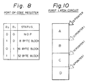
- the port OP code register (B0 , B1) is set to logic "1, 1", and according to the truth value table shown in Fig. 8, the output of GATE-820 becomes logic "1" and supplied to GATE-830.
- GATE-810 to GATE-813 the logical sum forming operation for the input signal and the output signal of the control table (E0 , E1 , E2 , E3) is carried out.
- the state of E0 , E1 , and E2 of the control table is logic "1, 1, 1”
- the output of GATE-830 becomes logic "1” through GATE-810 to GATE-813, and the output signal of GATE-86 is delivered to reset the control table (E0 , E1 , E2 , E3) so that the completion of the block access is acknowledged.
- the control table (E0 , E1 , E2 , E3) is constituted by flip-flop circuits of the set-priority type.
- the control table (E0 , E1 , E2 , E3) gives priority to the set operation. Accordingly, the control of the block access is achieved without logic delay.
- the system can be constituted by including at least one access request bus between the processor and the main storage corresponding to a unit data length, and at least one first request port, concerning an access request from the processor to the main storage, for setting an access request corresponding to an access request element which is an element having a unit data length or a length shorter than this unit data length, the order of the access request elements being designated with regard to the execution of a program of operation of the system, a selection of access bus according to address indication position of a request being carried out concerning the output signal of the first access port, and non-occurrence of a reversal of the order designated for execution of the program of the system being ensured in the case where a setting is carried out to a second access port corresponding to the access request bus.
- This embodiment will be explained with reference to Figs. 3, 7, 8, 9, 10, 11, and 12.
- the logical storage busy condition is checked to determine, for example, that an element 0 corresponding to access port A is busy, while elements 1, 2, and 3 are busy-released (i.e., priority is acquired).
- a busy-released status is marked by an asterisk. Since there is no conflict between the logical storage banks, the access requests of the elements 1, 2, and 3 for which busy conditions are released are transmitted to the main storage, as shown in CYCLE-2.
- CYCLE-2 since the logical storage bank busy condition for element 0 corresponding to access port A is not released, the status of CYCLE-2 is maintained.
- the subsequent elements 4, 5, 6, and 7 are not allowed be set in the second latch circuit 5, and thus the sequential order of the execution of program is maintained.
- CYCLE-4 In CYCLE-4, the pointer is moved successively to access ports B, C, D and A.
- the elements 4, 5, 6, and 7 are transmitted to the second latch circuit 5 where the logical storage bank busy conditions are checked, and thus the sequential order of the execution of program is maintained.
- a PORT SET ENABLE POINTA ⁇ AEN + POINTB ⁇ BEN ⁇ CEN ⁇ DEN ⁇ AEN ⁇ BCMTCH ⁇ ⁇ CDMTCH ⁇ ⁇ DAMTCH ⁇ ⁇ BDMTCH ⁇ ⁇ BAMTCH ⁇ ⁇ CAMTCH ⁇ + POINTC ⁇ CEN ⁇ DEN ⁇ AEN ⁇ DCMTCH ⁇ ⁇ CAMTCH ⁇ ⁇ DAMTCH ⁇ + POINTD ⁇ DEN ⁇ AEN ⁇ DAMTCH ⁇
- This setting condition equation (1) represents a condition of setting to the second latch circuits 5 to ensure the sequential order of execution of a program with regard to the access port A of the first latch circuit 2.
- "POINTA ⁇ AEN” represents a condition for enabling a setting of the element data of the access port A to the second latch circuit 5.
- AEN denotes that the bus corresponding to the destination address of element data set in access port A is “usable” or the access request occupying the bus in question is now “request-released”.
- the representations of "BEN”, “CEN” and “DEN” are similar.
- BCMTCH represents the bus conflict (bus match) from the first latch circuit 2 to the second latch circuit 5, preventing the transmission of an element of, for example, access port B to the second latch circuit 5.
- the representations of "CDMTCH”, “DAMTCH”, “BDMTCH”, “BAMTCH” and “CAMTCH” are similar.
- BCMTCH (inverted BCMTCH) and the like represents the non-existence of a bus conflict.
- the first term at the right side of the equation (1) represents the condition which enables the setting to the second latch circuit 5 when the pointer is directed to access port A
- the second term of the right side of equation (1) represents the condition which enables the setting to the second latch circuit 5 when the pointer is directed to access port B
- the third term of the right side of equation (1) represents the condition which enables the setting to the second latch circuit 5 when the pointer is directed to access port C
- the fourth term of the right side of equation (1) represents the condition which enables the setting to the second latch circuit 5 when the pointer is directed to access port D.
- the setting condition equations which represent the conditions of setting to the second latch circuit 5 to ensure the sequential order of execution of program, with regard to access ports B, C, and D of the first latch circuit 2 can be established in the same way.
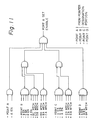
- FIG. 11 An example of the circuit for performing the setting condition equation is shown in Fig. 11.
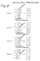
- FIG. 12 An example of the changes of designation by the pointer is shown in Fig. 12.
- the pointer In STEP-1, the pointer is directed to the access port A of the first latch circuit. Elements 0 and 1 satisfy the setting condition equation, and thus elements 0 and 1 are set to the second latch circuit, and accordingly, the pointer is moved to access port C.
Landscapes
- Engineering & Computer Science (AREA)
- Theoretical Computer Science (AREA)
- Physics & Mathematics (AREA)
- General Engineering & Computer Science (AREA)
- General Physics & Mathematics (AREA)
- Multi Processors (AREA)
Description
- The present invention relates to an access priority control system for a main storage for a computer. The system according to the present invention is used for access to a main storage for a computer in which the storage space of the main storage is hierarchically divided. The system according to the present invention can be used for control of an access priority order of a main storage in which a very high probability of existence of successive data of reading or writing, such as vector data, in the same divided storage space is utilized as in the multiple system.
- The system according to the present invention is applicable to a vector computer wherein a high speed vector calculation of scientific computation for carrying out a calculation in parallel or in the pipe-line manner is used, as well as to a general purpose computer.
- With regard to a main storage unit for a computer in which the storage space is divided into a plurality of segments having different buses and different storage banks, when an access request for read/write is received from a plurality of processors or other external devices, the priority order of the access requests must be determined and a bus conflict between the buses and a busy condition of the storage banks must be controlled.
- It is very important to reduce the length of the longest logic path of the control circuit for controlling the priority order and the busy condition checking in a predetermined cycle of the clock signal.
- Nevertheless, in the prior art system, the checking of the bus conflict, storage bank busy condition, and prohibition condition is carried out in a single cycle, and the determination of an approval of access to the main storage is carried out in that single cycle. Therefore, the checking of the bus conflict, storage bank busy condition, and prohibition condition must be carried out in a single cycle for all of the access parts, and accordingly, problems arise in that the delay time is very long and the amount of hardware needed is large.
- Also, in the prior art system, since the number of access ports is increased and the wirings cause a capacitance effect, the delay time of the longest logic path is increased, and accordingly, an extension of time is required, which has an undesirable effect on the selection of a machine cycle of the system.
- For an example of a prior art system corresponding substantially to the preamble of
claim 1, reference can be made to US-A-3 812 473. - It is an object of the present invention to provide an improved access priority control system for a main storage for a computer in which the delay time in a priority cycle is reduced, and the time for one clock cycle is reduced.
- It is another object of the present invention to reduce the amount of hardware needed for an access priority control system for a main storage for a computer.
- According to the present invention, the above objects are met by the access priority control system defined in
claim 1. - In the drawings,
- Fig. 1 shows a prior art access priority control system for a main storage for a computer;
- Fig. 2 shows the structure of a part of the logical storage busy check circuit used for the prior art system;
- Fig. 3 shows an access priority control system for a main storage for a computer according to the embodiments of the present invention;
- Fig. 4 shows a structure of the main storage unit in the system of Fig. 3;
- Fig. 5 shows a structure of a part of the logical storage busy check circuit used for the system of Fig. 3;
- Fig. 6 illustrates the transmission of access requests according to an embodiment of the present invention;
- Fig. 7 shows an arrangement of the priority acquisition control table in the priority acquisition control portion;
- Fig. 8 shows the truth value table of the port OP code register;
- Fig. 9 illustrates the operation of a system according to an embodiment of the present invention;
- Fig. 10 shows a sequence of access ports of the first latch circuits;
- Fig. 11 shows an example of the circuit for obtaining the setting condition equation; and
- Fig. 12 illustrates the changes of destination by the pointer.
- Before describing the embodiments of the present invention, a prior art access priority control system for a main storage for a computer is explained with reference to Figs. 1 and 2. In the prior art system of Fig. 1, there are provided central processor units CPU(0) 10, CPU(1) 11, CPU(2) 12, CPU(3) 13, and CPU(4) 14; a
first sequence 2 of latch circuits (LA) 20, 21, 22, 23, and 24, as a first sequence of access request ports; a busconflict check circuit 31; a logical storagebusy check circuit 32, a prohibitioncondition check circuit 33, a mainpriority control circuit 4′ ; asecond sequence 6 of latch circuits (LA) 600, 601, 602, 603, 610, 611, 612, and 613, as a second sequence of access request ports; and main storage units MSU(0) 70 and MSU(1) 71. - The main storage unit MSU(0) 70 is divided into a sequence of segments SEGMENT(0), SEGMENT(1), SEGMENT(2), and SEGMENT(3), and each of these segments is divided into, for example, 16 storage banks, which are called logical storages. The segments are connected with corresponding buses.
- The second sequence of
latch circuits 600 to 603 corresponds to the sequence of segments SEGMENT(0) TO SEGMENT(3). When a valid signal from the mainpriority control circuit 4′ is latched in thelatch circuit 6, use of a bus and a storage bank corresponding to the valid signal is approved. Each main storage unit is constituted by 4 segments, and each segment is constituted by 16 storage banks, and therefore, themain storage units - The busy check of the access to the storage banks is carried out such that a read and write cannot be carried out at a storage bank in the busy state, but a read and write can be carried out at a storage bank in the non-busy state.
- A non-busy storage bank must be selected when simultaneous accesses to two or more storage banks related to the same bus are required. Also, an unused bus must be selected, to avoid a bus conflict which might occur if a bus is required to transmit a plurality of data.
- In the prior art system of Fig. 1, the bus conflict check, the logical storage busy check, and the prohibition condition check are carried out simultaneously in the same cycle of a clock signal, and accordingly, the decision on whether or not the access to the main storage is approved is carried out in a single cycle.
- When a storage access request is received from an external device, the access request address signal is latched in the
latch circuit 2 in a given cycle, and the access request address signal is supplied to the busconflict check circuit 31 through a signal line, to the logical storagebusy check circuit 32 through a signal line, and to the prohibitioncondition check circuit 33 through a signal line, simultaneously, in the next cycle. The outputs of the busconflict check circuit 31, the logical storagebusy check circuit 32, and the prohibitioncondition check circuit 33 are supplied to the mainpriority control circuit 4′ in the same priority cycle, and the resulting output of the mainpriority control circuit 4′ is set in thelatch circuit 6. - The address signal to be latched in the
latch circuit 2 is, for example, an address signal of seven bits: A6, A5, A4, A3, A2, A1, A0, which can access one of 128 storage banks. The A6 bit designates one of themain storage units - The bus
conflict check circuit 31 is supplied with the upper address bits: A6, A5, A4 of the address signal, checks whether or not the supplied address bits coincide with the code corresponding to the bus being used, and delivers a coincidence/non-coincidence signal to be supplied to the mainpriority control circuit 4′ through a signal line. - The logical storage
busy check circuit 32 is supplied with the entire 7 bits: A6 to A0, of the address signal, decodes the supplied address bits, checks whether or not the decoded 128 signals coincide with the busy signals indicating busy states of the 128 storage banks, and delivers a coincidence/non-coincidence signal to be supplied to the mainpriority control circuit 4′ through a signal line. - The prohibition
condition check circuit 33 is supplied with the address signal, decodes the supplied address bits, compares the decoded signal with the prohibition condition signal to produce a coincidence/non-coincidence signal, and supplies the produced coincidence/non-coincidence signal to the mainpriority control circuit 4′ through a signal line. - In the prior art system of Fig. 1, in the request transfer cycle, a memory access request from the central processor unit or other external device is carried out; in the next priority cycle, a checking of all conflict conditions and prohibition conditions for all access ports and a checking of all priority orders are carried out, based on the setting of a request address in the
latch circuit 2; and, in the next main storage unit transmitting cycle, a memory access is started based on the setting of the signal determined in the above-mentioned next priority cycle in thelatch circuit 6. - The structure of a part of a prior art logical storage
busy check circuit 32 used for the prior art system of Fig. 1 is shown in Fig. 2. The logical storage busy check circuit of Fig. 2 is constituted by a sequence of GATE-00 to GATE-07, a sequence of GATE-10 to GATE-13, GATE-2, GATE-3, GATE-4, and GATE-5. Each of the GATE-00 to GATE-07, GATE-10 to GATE-13, GATE-3, and GATE-5 is constituted by an emitter coupled logic (ECL) circuit. The address signal of 7 bits: A6, A5, A4, A3, A2, A1, A0 is supplied to GATE-00 through GATE-07. GATE-2 and GATE-4 are emitter dot type OR gates and do not cause delay problems. - GATE-00 and GATE-01 are supplied with a 7 bit address signal: A6, A5, A4, A3, A2, A1, A0 as an input signal, which signal comprises all logic "0's" when the address A6, A5, A4, A3, A2, A1, A0 is logic "0, 0, 0, 0, 0, 0, 0"; GATE-02 and GATE-03 are supplied with a 7 bit address signal, which signal comprises all logic "0 s" when the address: A6, A5, A4, A3, A2, A1, A0 is logic "0, 0, 0, 0, 0, 0, 1"; GATE-04 and GATE-05 are supplied with a 7 bit address signal, which signal comprises all logic "0's" when the address: A6, A5, A4, A3, A2, A1, A0 is logic "0, 0, 0, 0, 0, 1, 0"; and GATE-06 and GATE-07 are supplied with a 7 bit address signal, which signal comprises all logic "0,s" when the address: A6, A5, A4, A3, A2, A1, A0 is logic "0, 0, 0, 0, 0, 1, 1". Although only a part of the logical storage busy check circuit is shown in Fig. 2, there are actually 128 gate pairs including the shown 4 gate pairs GATE-00 and GATE-01; GATE-02 and GATE-03; GATE-04 and GATE-05; and GATE-06 and GATE-07, so that, in practice, the extent of circuit of the logical storage busy check circuit is 32 times that of the Fig. 2 circuit. The logic "0" outputs of GATE-00 and GATE-01, which are delivered when all of the input signal to GATE-00 and GATE-01 are logic "0's", are supplied to GATE-10, and GATE-10 delivers a logic "1" when the signals supplied from GATE-00 and GATE-01 are logic "0, 0" and the busy signal: BUSY(0) is logic "0". GATE-11, GATE-12, and GATE-13 operate in the same manner.
- Assuming that the delay time per unit gate is τ, the delay time of the logical storage busy check circuit of Fig. 2 is 4τ. There are 393 gates for one port, and when 5 ports exist, the number of gates is 393 x 5 = 1965, which is very large number. The busy checks must be carried out in parallel for request for a plurality of
ports 2, and accordingly, a number of circuits of Fig. 2 corresponding to the number of theports 2, must be provided. - An access priority control system for a main storage for a computer according to an embodiment of the present invention will be explained with reference to Fig. 3.
- It should be noted that, in Fig. 3 as well as in Fig. 1, only signal lines for a priority control in question are drawn between the blocks and illustration of address buses and data buses is omitted for convenience. Also, only signal lines for start signals for storage segments are drawn from the
third latch circuit 6 to thestorage segments - The system of Fig. 3 is constituted by a sequence of central processor units (CPU) 10 to 14, a
first sequence 2 of latch circuits (LA) 20 to 24 as a first sequence of access ports, a bus conflict check and prohibitioncondition check circuit 3, asecond sequence 5 of latch circuits (LA) 500 to 503 and 510 to 513 as a second sequence of access ports, asequence 4 of logical storagebusy check circuits 400t0 third sequence 6 oflatch circuits 600 to 603 and 610 to 613, and main storage units (MSU) 70 to 71. - Each of the main storage units is divided into segments: SEGMENT(0) to SEGMENT(3), and each of the segments is divided into, for example, 16 storage banks, as logical storages as shown in Fig. 4. The third sequence of
latch circuits 600 to 603 and 610 to 613 corresponds to the segments of themain storage units latch circuits 600 to 603 and 610 to 613, use of a storage bank corresponding to the valid signal is approved. - Each of the
main storage units main storage units - The logical storage
busy check circuit 4 decodes the lower 4 bit address A3, A2, A1, A0 as an intra-segment address latched in thesecond latch circuit 5, and checks whether or not the decoded signal coincides with the busy signal. When it is determined to be in the busy state the read/write operation of the storage bank in question is not approved, but when it is determined to be in the non-busy state, the read/write operation of the storage bank in question is approved. - In the system of Fig. 3, when a conflict occurs between a plurality of requests on one segment, one request is selected in the bus conflict check and prohibition
condition check circuit 3, and this selected request is supplied to a logical storagebusy check circuit 4. Accordingly, in a segment correspondence portion of the logical storagebusy check circuit 4, no conflict occurs between a plurality of requests and a request is always delivered to a storage segment unless a busy state is detected. - In the system of Fig. 3, the checking by the bus conflict check and prohibition
condition check circuit 3 is carried out in a first priority cycle, to select a bus, and the storage bank busy checking by the logical storagebusy check circuit 4 is carried out in a second priority cycle. - In the system of Fig. 3, in the first priority cycle, the bus conflict check and prohibition
condition check circuit 3, using the upper address bits: A6, A5, A4 set in thefirst latch circuit 2, carries out the bus selection based on the checking of the bus conflict. - This checking is carried out to determine whether or not the lower 4 address bits as the intra-segment address bits: A3, A2, A1, A0 can be set in the
second latch circuit 5, and the setting of the lower 4 address bits: A3, A2, A1, A0, to thesecond latch circuit 5 is carried out. Then, in the second priority cycle, the logical storagebusy check circuit 4 checks the intra-segment conflict condition, and a determination of the transmission of the request to the main storage unit based on the result of the checking is carried out. - The setting of the request address to the
first latch circuit 2 in the first priority cycle can be carried out in the request transfer cycle. - In the system of Fig. 3, when a memory access request is received from an external device, the upper 3 bits: A6, A5, A4, designating one of eight buses of the 7 bit address for designating one of the 128 storage banks: A6, A5, A4, A3, A2, A1, A0, are set in the
first latch circuit 2. The bus conflict check and prohibitioncondition check circuit 3 receives this upper 3 bit address: A6, A5, A4, compares the upper 3 bit address: A6, A5, A4 with the code corresponding to the bus under use by the 3 bit comparison member to detect whether or not a coincidence exists, and determines whether or not the requested bus among the 8 buses corresponding to the 8 segments can be used. - When the requested bus can be used, the selection of this requested bus is carried out. When the requested bus in question is being used for other access requests, the request in question must wait until the use by the other access request is terminated and the use of the requested bus is approved.
- Nevertheless, since in the case of the processing of vector data, after the use of a bus is approved, usually the probability of a subsequent access request for the same bus is very high, the selection first of the bus will not have an adverse affect on the performance of the system.
- Since the bus conflict check and prohibition
condition check circuit 3 is constituted basically by comparator members, the length of the longest logic path of thiscircuit 3 is relatively short, and the amount of hardware needed for thiscircuit 3 is relatively small. - In the system of Fig. 3, the logical storage
busy check circuit 4 decodes the lower 4 bit address; A3, A2, A1, A0 for designating one of 16 storage banks, and compares the decoded signal with the busy signal. - The logical storage
busy check circuit 4 can be constituted such that the amount of hardware needed is much less than needed by the prior art logical storage busy check circuit, and the length of the longest logic path is much shorter than that of the prior art logical storage busy check circuit. - The structure of the logical storage
busy check circuit 4 used for the system of Fig. 3 is shown in Fig. 5. The logical storage busy check circuit of Fig. 5 is constituted by a sequence of GATE-00 to GATE-03, a sequence of GATE-10 to GATE-13, a sequence of GATE-20 to GATE-23, and GATE-3. - In the logical storage busy check circuit of Fig. 5, the supplied 4 bit address: A3, A2, A1, A0 is decoded, and it is determined whether or not the 16 decoded signals coincide with the busy signal for the 16 storage banks in a segment.
- Each of GATE-00 to GATE-03, GATE-10 to GATE-13, and GATE-20 to GATE-23 is constituted by an emitter coupled logic circuit. GATE-3 is an emitter dot type OR gate.
- The input signal: +ADDRESS BIT(A0), +ADDRESS BIT(A1), +ADDRESS BIT(A2), +ADDRESS BIT(A3), for GATE-00, is a signal having all logic "0 s" when the address "A0, A1, A2, A3" is logically "0, 0, 0, 0"; the input signal: +ADDRESS BIT(A0), +ADDRESS BIT(A1), +ADDRESS BIT(A2), -ADDRESS BIT(A3), for GATE-01 is a signal having all logic "0,s" when the address "A0, A1, A2, A3" is logically "0, 0, 0, 1"; the input signal: +ADDRESS BIT(A0), +ADDRESS BIT(A1), -ADDRESS BIT(A2), +ADDRESS BIT(A3), for GATE-02, is a signal having all logic "0's" when the address "A0, A1, A2, A3" is "0, 0, 1, 0"; and the input signal: +ADDRESS BIT(A0), +ADDRESS BIT(A1), -ADDRESS BIT(A2), -ADDRESS BIT(A3), for GATE-03, is a signal having all logic "0's" when the address "A0, A1, A2, A3" is "0, 0, 1, 1".
- Although 4 gates: GATE-00, GATE-01, GATE-02 GATE-03 are shown as a first sequence in Fig. 5, 16 gates in all exist for all of the segments.
- GATE-00 delivers an output "0" when the input signal: +ADDRESS BIT(A0), +ADDRESS BIT(A1), +ADDRESS BIT(A2), +ADDRESS BIT(A3), are all logic "0's", and the delivered output is supplied to GATE-10. GATE-10 delivers an output "1" when one input supplied from GATE-10 is "0" and the other input of -BUSY(0) is "0".
- The output signals of GATE-10 to GATE-13 are supplied to GATE-20. The output signal of GATE-20 is a signal which is logic "1" when at least one of the output signals of GATE-10 to GATE-13 is logic "1". In the device of Fig. 5, there are 4 gates: GATE-20, GATE-21, GATE-22, GATE-23, and the output signals of these 4 gates are supplied to an emitter dot type OR gate: GATE-03. A check is made to detect a coincidence between the decoded 16 signals and the busy signal of 16 storage banks in a segment, and it is not necessary for a gate to be connected to the output terminal of GATE-3.
- The comparison of the delay time, the number of gates per unit, and the total number of gates between the device of Fig. 5 and the device of Fig. 2 (prior art) is as follows. The delay time is 3τ for the device of Fig. 5, but 4τ for the device of Fig. 2 where τ is the delay time for a unit gate.
- There are 36 gates per unit for the device of Fig. 5, and 393 gates per unit for the device of Fig. 2. The total number is 36 x 16 = 576 (16 buses) for the device of Fig. 5, and 393 x 5 = 1965 (5 ports) for the device of Fig. 2.
- This comparison shows that the delay time in the cycle of priority determination and the amount of hardware are reduced in the device of Fig. 5 according to an embodiment of the present invention.
- As another embodiment of the present invention, the system can be constituted by including at least one access request bus between the processor and the main storage corresponding to a unit data length, an access request from the processor to the main storage being transmitted with the unit data length or a multiple of the unit data length, and a block access from the processor to the main storage being divided into a plurality of smaller access units corresponding to the unit data length in the processor. This embodiment will be explained with reference to Figs. 3, 4, 5, 6, 7, and 8.
- The transmission of access requests is illustrated in Fig. 6.
- It is assumed that the data of a block access of an access request from a processor is constituted by a sequence of elements (unit data): 0, 1, 2, 3, 4, 5, 6, 7. In CYCLE-1 of the
second latch circuit 5, the logical storage bank busy condition is released (i.e., priority is acquired) forelement 0 andelement 2, and thus the access request can be transmitted. Since there is no logical storage bank conflict in CYCLE-1, the elements which have acquired priority are transmitted to the main storage. - In CYCLE-2, the logical storage bank busy condition is released for
element 1 andelement 3, and since theelement 1 andelement 3 have acquired priority, they are transmitted to the main storage. - Accordingly, in CYCLE-3, the logical storage bank busy condition is checked for the subsequent sequence of
elements - In the block access transmitted with a multiple of unit data length, to maintain the regular order of transmitting a plurality of unit data constituting the block, the completion of the block access in question, i.e., the completion of transmitting of the data block, is acknowledged by a priority acquisition control table in a priority acquisition control portion.
- The arrangement of the priority acquisition control table in the priority acquisition control portion is shown in Fig. 7.
- When priorities are acquired for access requests from the
second latch circuit 5 in the second priority cycle, logic "1" is transmitted to the priority acquisition table. In the device of Fig. 7, it is assumed that the block access is carried out for, for example, an 8 byte block, a 16 byte block, or a 32 byte block. - In the case of a 32 byte block access in the device of Fig. 7, the port OP code register (B₀ , B₁) is set to logic "1, 1", and according to the truth value table shown in Fig. 8, the output of GATE-820 becomes logic "1" and supplied to GATE-830.
- Then, priority is acquired for the access request signal from the
second latch circuit 5, and when the elements E₀ , E₁ , E₂ , and E₃ of the control table become all logic "1's", it is acknowledged that a 32 byte block access request has been transmitted, the output of GATE-830 becomes logic "1" through the operations of GATE-810 to GATE-813, and an output signal is delivered from GATE-86 to reset the priority acquisition control table. - In GATE-810 to GATE-813, the logical sum forming operation for the input signal and the output signal of the control table (E₀ , E₁ , E₂ , E₃) is carried out. Assuming that the state of E₀ , E₁ , and E₂ of the control table is logic "1, 1, 1", when a priority of access request signal corresponding to element No. 3 (corresponding to E₃) is received in the next cycle, the output of GATE-830 becomes logic "1" through GATE-810 to GATE-813, and the output signal of GATE-86 is delivered to reset the control table (E₀ , E₁ , E₂ , E₃) so that the completion of the block access is acknowledged.
- The above operations are similar in the case of a 16 byte block access or an 8 byte block access.
- The control table (E₀ , E₁ , E₂ , E₃) is constituted by flip-flop circuits of the set-priority type. When a priority acquisition signal for the next access request is supplied from the
second latch circuit 5 while the above-mentioned control table resetting signal is being delivered, the control table (E₀ , E₁ , E₂ , E₃) gives priority to the set operation. Accordingly, the control of the block access is achieved without logic delay. - As still another embodiment of the present invention, the system can be constituted by including at least one access request bus between the processor and the main storage corresponding to a unit data length, and at least one first request port, concerning an access request from the processor to the main storage, for setting an access request corresponding to an access request element which is an element having a unit data length or a length shorter than this unit data length, the order of the access request elements being designated with regard to the execution of a program of operation of the system, a selection of access bus according to address indication position of a request being carried out concerning the output signal of the first access port, and non-occurrence of a reversal of the order designated for execution of the program of the system being ensured in the case where a setting is carried out to a second access port corresponding to the access request bus. This embodiment will be explained with reference to Figs. 3, 7, 8, 9, 10, 11, and 12.
- The operation of the system according to this embodiment is explained with reference to Fig. 9, as follows. It is assumed that a sequence of element data: 0, 1, 2, 3 is set in the
first latch circuit 2, in the first priority cycle, as sequence-1. The bus conflict checkings for this element data: 0, 1, 2, 3 are carried out, and based on the access port number indicated by the pointer, the element data, which has passed the bus conflict checkings, is set to thesecond latch circuit 5 as CYCLE-1, the sequential order of the execution of program being ensured. - In the second priority cycle, the logical storage busy condition is checked to determine, for example, that an
element 0 corresponding to access port A is busy, whileelements elements - In CYCLE-2, since the logical storage bank busy condition for
element 0 corresponding to access port A is not released, the status of CYCLE-2 is maintained. Thesubsequent elements second latch circuit 5, and thus the sequential order of the execution of program is maintained. - In CYCLE-3, the logical storage bank busy condition for
element 0 corresponding to access port A is released, and thiselement 0 is transmitted to the main storage. But, since the pointer is still directed to access port A, a setting of thesubsequent elements - In CYCLE-4, the pointer is moved successively to access ports B, C, D and A. The
elements second latch circuit 5 where the logical storage bank busy conditions are checked, and thus the sequential order of the execution of program is maintained. - An example of the setting condition equation of the control of the request pointer with regard to a sequence of the first access ports: A, B, C, and D shown in Fig. 10 is as follows.

- This setting condition equation (1) represents a condition of setting to the
second latch circuits 5 to ensure the sequential order of execution of a program with regard to the access port A of thefirst latch circuit 2. - "POINTA·AEN" represents a condition for enabling a setting of the element data of the access port A to the
second latch circuit 5. "AEN" denotes that the bus corresponding to the destination address of element data set in access port A is "usable" or the access request occupying the bus in question is now "request-released". The representations of "BEN", "CEN" and "DEN" are similar. - "BCMTCH" represents the bus conflict (bus match) from the
first latch circuit 2 to thesecond latch circuit 5, preventing the transmission of an element of, for example, access port B to thesecond latch circuit 5. The representations of "CDMTCH", "DAMTCH", "BDMTCH", "BAMTCH" and "CAMTCH" are similar. - Assuming that the pointer is directed to access port B of the
first latch circuit 2, where "BEN", "CEN", "DEN", and "AEN", which are destination conditions of element data of access ports B, C, D and A, are all "usable" or "request-released", and no bus conflicts exist concerning thesecond latch circuit 5, the element data of access port A of thefirst latch circuit 2 can be set to thesecond latch circuit 5. - "
BCMTCH " (inverted BCMTCH) and the like represents the non-existence of a bus conflict. - In setting the condition equation (1), the first term at the right side of the equation (1) represents the condition which enables the setting to the
second latch circuit 5 when the pointer is directed to access port A, the second term of the right side of equation (1) represents the condition which enables the setting to thesecond latch circuit 5 when the pointer is directed to access port B, the third term of the right side of equation (1) represents the condition which enables the setting to thesecond latch circuit 5 when the pointer is directed to access port C, and the fourth term of the right side of equation (1) represents the condition which enables the setting to thesecond latch circuit 5 when the pointer is directed to access port D. - The setting condition equations which represent the conditions of setting to the
second latch circuit 5 to ensure the sequential order of execution of program, with regard to access ports B, C, and D of thefirst latch circuit 2 can be established in the same way. - An example of the circuit for performing the setting condition equation is shown in Fig. 11.
- An example of the changes of designation by the pointer is shown in Fig. 12. In STEP-1, the pointer is directed to the access port A of the first latch circuit.
Elements elements - In STEP-2,
elements B. Elements elements - In STEP-3,
elements A. Elements 5 satisfies the setting condition equation, and is set to the second latch circuit, and accordingly, the pointer is moved to access port C to proceed to STEP-4.
Claims (11)
- An access priority control system for a main storage (70,71) for a computer, for controlling a signal transmission to the main storage upon receiving a plurality of storage access requests from at least one processor (10-14) related to the main storage, said system comprising:
first access request port means (20-24) for holding at least temporarily a segment address of the storage access requests from the processor;
characterized in that it further comprises :
first control means (3) responsive to the output of said first access request port means for checking bus conflict conditions and prohibition conditions for a destination storage segment determined by the address of the storage access request;
second access request port means (500-503; 510-513) responsive to the output of said first control means for holding at least temporarily an intra-segment address of said storage access request; and
second control means (400-403 ; 410-413) responsive to the output of said second access request port means for checking logical storage busy conditions in the storage segments,
wherein the checking of the bus conflict condition and the prohibition condition and the checking of the logical storage busy condition are carried out in different clock cycles. - A system according to claim 1, wherein said first control means comprises a comparator circuit for comparing the segment address of the storage access request with the segment address indicating a bus-in-use state.
- A system according to claim 1, wherein said second control means (400-403 ; 410-413) is a busy check circuit for decoding the intra-segment address of the storage access request and checking the coincidence between the decoded signal and a busy signal for the storage banks of the main storage (70,71).
- A system according to claim 1, wherein a cycle in which the checking by said first control means (3) is carried out corresponds to a request transfer cycle.
- A system according to any one of claims 1 to 4, further comprising at least one access request bus between the processor and the main storage corresponding to a unit data length,
an access request from the processor to the main storage (70,71) being transmitted with the unit data length or a multiple of the unit data length,
a block access from the processor (10-14) to the main storage being divided into a plurality of smaller access units corresponding to the unit data length in the processor. - A system according to claim 5, wherein an access request is transmitted to the main storage (70,71) for each unit data length so that the transmitting orders of block accesses are optionally controlled.
- A system according to claim 5, wherein said first control means for the processor check bus conflicts between the first access request ports corresponding to segments of the main storage (70,71) and said second control means for the processor (10-14) check logical storage busy conditions,
a checking of conflicts between buses corresponding to the first access request ports being carried out by said first control means,
a checking of busy conditions of logical storage banks for each bus being carried out by said second control means,
an access request being transmitted to a logical storage bank for each unit data when the result of the busy condition checking indicates a non-busy state. - A system according to claim 5, wherein said system comprises priority acquisition control table means (81) for controlling a priority acquisition for unit data from each first access request port in the second priority cycle,
a completion of transmitting of all unit data of a block constituted by a plurality of unit data from the first access request ports being detected according to priority information for each unit data of said priority acquisition control table means,
a completion of the block access being determined on the basis of the results of said detection of a completion of all unit data transmitting. - A system according to claim 1, further comprising at least one access request bus between the processor (10-14) and the main storage (70,71) corresponding to a unit data length, and at least one first access request port, for an access request from the processor (10-14) to the main storage, for setting an access request corresponding to an access request element which is an element having a unit data length or a length shorter than this unit data length,
the order of the access request elements being designated with regard to the execution of a program of operation of the system,
a selection of access bus according to address indication position of a request being carried out concerning the output signal of the first access request port,
non-occurrence of a reversal of the order designated for execution of the program of the system being ensured where a setting is carried out to a second access request port corresponding to the access request bus. - A system according to claim 9, wherein a checking of conflicts only in an access request bus in question is carried out for the output signal of the second access request port, to determine whether or not a transmitting of an access request in question is approved.
- A system according to claim 9, wherein said first control means set access requests in the second access request port in the regular sequence in accordance with a result of a checking of bus conflicts between the first access request ports corresponding to main storage segments and a pointer (82) for designating an order in a program execution sequence, and said second control means check logical storage busy conditions for unit data in main storage segments,
an access request being selected and set in the second access request port by the first control means by giving the highest priority to the result of conflict checking between buses corresponding to the first access request ports and to the port designation by the pointer,
a logical storage bank busy checking in a bus in question being carried out for each second access request port by the second control means, and, when the result of the logical storage bank busy checking indicates a non-busy state, a transmitting of access request for each unit data is carried out.
Applications Claiming Priority (6)
| Application Number | Priority Date | Filing Date | Title |
|---|---|---|---|
| JP23370487A JPS6478337A (en) | 1987-09-19 | 1987-09-19 | Control system for main memory access priority order |
| JP233704/87 | 1987-09-19 | ||
| JP62256794A JPH0199143A (en) | 1987-10-12 | 1987-10-12 | Main memory access control system |
| JP256794/87 | 1987-10-12 | ||
| JP62314745A JPH0610801B2 (en) | 1987-12-10 | 1987-12-10 | Main memory access controller |
| JP314745/87 | 1987-12-10 |
Publications (3)
| Publication Number | Publication Date |
|---|---|
| EP0309330A2 EP0309330A2 (en) | 1989-03-29 |
| EP0309330A3 EP0309330A3 (en) | 1991-05-08 |
| EP0309330B1 true EP0309330B1 (en) | 1994-11-30 |
Family
ID=27332027
Family Applications (1)
| Application Number | Title | Priority Date | Filing Date |
|---|---|---|---|
| EP88402360A Expired - Lifetime EP0309330B1 (en) | 1987-09-19 | 1988-09-19 | Access priority control system for main storage for computer |
Country Status (6)
| Country | Link |
|---|---|
| US (1) | US5073871A (en) |
| EP (1) | EP0309330B1 (en) |
| AU (1) | AU592717B2 (en) |
| CA (1) | CA1310429C (en) |
| DE (1) | DE3852261T2 (en) |
| ES (1) | ES2064364T3 (en) |
Families Citing this family (11)
| Publication number | Priority date | Publication date | Assignee | Title |
|---|---|---|---|---|
| US5214769A (en) * | 1987-12-24 | 1993-05-25 | Fujitsu Limited | Multiprocessor control system |
| JPH01169565A (en) * | 1987-12-24 | 1989-07-04 | Fujitsu Ltd | Multiprocessor control system |
| JPH01303543A (en) * | 1988-05-31 | 1989-12-07 | Fujitsu Ltd | Memory access control system |
| FR2644260B1 (en) * | 1989-03-08 | 1993-10-29 | Nec Corp | MEMORY ACCESS CONTROL DEVICE FOR SIMPLE CONTROL |
| KR930002316B1 (en) * | 1989-05-10 | 1993-03-29 | 미쯔비시덴끼 가부시끼가이샤 | Bus control method and image processing device |
| JPH0648477B2 (en) * | 1990-09-17 | 1994-06-22 | 日通工株式会社 | Bus acquisition method in multiprocessor system |
| US5515523A (en) * | 1991-06-03 | 1996-05-07 | Digital Equipment Corporation | Method and apparatus for arbitrating conflicts by monitoring number of access requests per unit of time in multiport memory systems |
| US5423008A (en) * | 1992-08-03 | 1995-06-06 | Silicon Graphics, Inc. | Apparatus and method for detecting the activities of a plurality of processors on a shared bus |
| JP3010947B2 (en) * | 1992-11-26 | 2000-02-21 | 日本電気株式会社 | Memory access control device |
| US6055607A (en) * | 1996-12-23 | 2000-04-25 | Unisys Corporation | Interface queue with bypassing capability for main storage unit |
| DE10110578B4 (en) * | 2000-03-29 | 2004-06-03 | International Business Machines Corporation | Hierarchical priority filter with integrated serialization |
Family Cites Families (7)
| Publication number | Priority date | Publication date | Assignee | Title |
|---|---|---|---|---|
| US3812473A (en) * | 1972-11-24 | 1974-05-21 | Ibm | Storage system with conflict-free multiple simultaneous access |
| US4212057A (en) * | 1976-04-22 | 1980-07-08 | General Electric Company | Shared memory multi-microprocessor computer system |
| US4314335A (en) * | 1980-02-06 | 1982-02-02 | The Perkin-Elmer Corporation | Multilevel priority arbiter |
| US4395753A (en) * | 1980-06-26 | 1983-07-26 | Gte Automatic Electric Labs Inc. | Allocation controller providing for access of multiple common resources by a plurality of central processing units |
| US4445174A (en) * | 1981-03-31 | 1984-04-24 | International Business Machines Corporation | Multiprocessing system including a shared cache |
| US4875161A (en) * | 1985-07-31 | 1989-10-17 | Unisys Corporation | Scientific processor vector file organization |
| JPH0628051B2 (en) * | 1986-04-25 | 1994-04-13 | 株式会社日立製作所 | Memory control method |
-
1988
- 1988-09-15 CA CA000577485A patent/CA1310429C/en not_active Expired - Lifetime
- 1988-09-16 AU AU22318/88A patent/AU592717B2/en not_active Ceased
- 1988-09-19 US US07/246,087 patent/US5073871A/en not_active Expired - Lifetime
- 1988-09-19 ES ES88402360T patent/ES2064364T3/en not_active Expired - Lifetime
- 1988-09-19 EP EP88402360A patent/EP0309330B1/en not_active Expired - Lifetime
- 1988-09-19 DE DE3852261T patent/DE3852261T2/en not_active Expired - Fee Related
Also Published As
| Publication number | Publication date |
|---|---|
| DE3852261D1 (en) | 1995-01-12 |
| CA1310429C (en) | 1992-11-17 |
| ES2064364T3 (en) | 1995-02-01 |
| AU2231888A (en) | 1989-05-04 |
| US5073871A (en) | 1991-12-17 |
| AU592717B2 (en) | 1990-01-18 |
| EP0309330A2 (en) | 1989-03-29 |
| DE3852261T2 (en) | 1995-04-06 |
| EP0309330A3 (en) | 1991-05-08 |
Similar Documents
| Publication | Publication Date | Title |
|---|---|---|
| US5016167A (en) | Resource contention deadlock detection and prevention | |
| US4600986A (en) | Pipelined split stack with high performance interleaved decode | |
| US4481572A (en) | Multiconfigural computers utilizing a time-shared bus | |
| US4500958A (en) | Memory controller with data rotation arrangement | |
| US4371928A (en) | Interface for controlling information transfers between main data processing systems units and a central subsystem | |
| US4195342A (en) | Multi-configurable cache store system | |
| CA1184311A (en) | Peripheral interface adapter circuit for use in i/o controller card having multiple modes of operation | |
| US5293500A (en) | Parallel processing method and apparatus | |
| US4675812A (en) | Priority circuit for channel subsystem having components with diverse and changing requirement for system resources | |
| EP0450233A2 (en) | Bus access for digital computer system | |
| EP0515165B1 (en) | A Memory access device | |
| US5142638A (en) | Apparatus for sharing memory in a multiprocessor system | |
| JPS6327738B2 (en) | ||
| EP0170021B1 (en) | Data processing system with a plurality of processors accessing a common bus to interleaved storage | |
| US6026451A (en) | System for controlling a dispatch of requested data packets by generating size signals for buffer space availability and preventing a dispatch prior to a data request granted signal asserted | |
| US4371924A (en) | Computer system apparatus for prefetching data requested by a peripheral device from memory | |
| US4843543A (en) | Storage control method and apparatus | |
| US20040177231A1 (en) | Data processor | |
| US4509115A (en) | Two-port memory controller | |
| US5073871A (en) | Main storage access priority control system that checks bus conflict condition and logical storage busy condition at different clock cycles | |
| US4697233A (en) | Partial duplication of pipelined stack with data integrity checking | |
| EP0245029A2 (en) | High speed memory systems | |
| US4441152A (en) | Data processing system having ring-like connected multiprocessors relative to key storage | |
| US5742842A (en) | Data processing apparatus for executing a vector operation under control of a master processor | |
| US5568631A (en) | Multiprocessor system with a shared control store accessed with predicted addresses |
Legal Events
| Date | Code | Title | Description |
|---|---|---|---|
| PUAI | Public reference made under article 153(3) epc to a published international application that has entered the european phase |
Free format text: ORIGINAL CODE: 0009012 |
|
| AK | Designated contracting states |
Kind code of ref document: A2 Designated state(s): DE ES FR GB |
|
| PUAL | Search report despatched |
Free format text: ORIGINAL CODE: 0009013 |
|
| AK | Designated contracting states |
Kind code of ref document: A3 Designated state(s): DE ES FR GB |
|
| 17P | Request for examination filed |
Effective date: 19911008 |
|
| 17Q | First examination report despatched |
Effective date: 19930201 |
|
| GRAA | (expected) grant |
Free format text: ORIGINAL CODE: 0009210 |
|
| AK | Designated contracting states |
Kind code of ref document: B1 Designated state(s): DE ES FR GB |
|
| REF | Corresponds to: |
Ref document number: 3852261 Country of ref document: DE Date of ref document: 19950112 |
|
| REG | Reference to a national code |
Ref country code: ES Ref legal event code: FG2A Ref document number: 2064364 Country of ref document: ES Kind code of ref document: T3 |
|
| ET | Fr: translation filed | ||
| PLBE | No opposition filed within time limit |
Free format text: ORIGINAL CODE: 0009261 |
|
| STAA | Information on the status of an ep patent application or granted ep patent |
Free format text: STATUS: NO OPPOSITION FILED WITHIN TIME LIMIT |
|
| 26N | No opposition filed | ||
| PGFP | Annual fee paid to national office [announced via postgrant information from national office to epo] |
Ref country code: ES Payment date: 19980921 Year of fee payment: 11 |
|
| PG25 | Lapsed in a contracting state [announced via postgrant information from national office to epo] |
Ref country code: ES Free format text: LAPSE BECAUSE OF NON-PAYMENT OF DUE FEES Effective date: 19990920 |
|
| REG | Reference to a national code |
Ref country code: GB Ref legal event code: IF02 |
|
| PGFP | Annual fee paid to national office [announced via postgrant information from national office to epo] |
Ref country code: FR Payment date: 20030909 Year of fee payment: 16 |
|
| PGFP | Annual fee paid to national office [announced via postgrant information from national office to epo] |
Ref country code: GB Payment date: 20030917 Year of fee payment: 16 |
|
| PGFP | Annual fee paid to national office [announced via postgrant information from national office to epo] |
Ref country code: DE Payment date: 20031002 Year of fee payment: 16 |
|
| REG | Reference to a national code |
Ref country code: ES Ref legal event code: FD2A Effective date: 20001013 |
|
| PG25 | Lapsed in a contracting state [announced via postgrant information from national office to epo] |
Ref country code: GB Free format text: LAPSE BECAUSE OF NON-PAYMENT OF DUE FEES Effective date: 20040919 |
|
| PG25 | Lapsed in a contracting state [announced via postgrant information from national office to epo] |
Ref country code: DE Free format text: LAPSE BECAUSE OF NON-PAYMENT OF DUE FEES Effective date: 20050401 |
|
| GBPC | Gb: european patent ceased through non-payment of renewal fee |
Effective date: 20040919 |
|
| PG25 | Lapsed in a contracting state [announced via postgrant information from national office to epo] |
Ref country code: FR Free format text: LAPSE BECAUSE OF NON-PAYMENT OF DUE FEES Effective date: 20050531 |
|
| REG | Reference to a national code |
Ref country code: FR Ref legal event code: ST |