EP0304032B1 - Light controlled thyristor - Google Patents
Light controlled thyristor Download PDFInfo
- Publication number
- EP0304032B1 EP0304032B1 EP88113350A EP88113350A EP0304032B1 EP 0304032 B1 EP0304032 B1 EP 0304032B1 EP 88113350 A EP88113350 A EP 88113350A EP 88113350 A EP88113350 A EP 88113350A EP 0304032 B1 EP0304032 B1 EP 0304032B1
- Authority
- EP
- European Patent Office
- Prior art keywords
- zone
- auxiliary emitter
- electrode
- base
- auxiliary
- Prior art date
- Legal status (The legal status is an assumption and is not a legal conclusion. Google has not performed a legal analysis and makes no representation as to the accuracy of the status listed.)
- Expired - Lifetime
Links
- 239000003990 capacitor Substances 0.000 claims description 22
- 239000004065 semiconductor Substances 0.000 claims description 13
- 238000010276 construction Methods 0.000 claims 2
- 238000006073 displacement reaction Methods 0.000 description 8
- 239000004020 conductor Substances 0.000 description 3
- 206010034960 Photophobia Diseases 0.000 description 1
- 206010034972 Photosensitivity reaction Diseases 0.000 description 1
- 230000000903 blocking effect Effects 0.000 description 1
- 230000015556 catabolic process Effects 0.000 description 1
- 239000002800 charge carrier Substances 0.000 description 1
- 230000002349 favourable effect Effects 0.000 description 1
- 208000013469 light sensitivity Diseases 0.000 description 1
- 230000036211 photosensitivity Effects 0.000 description 1
Images


Classifications
-
- H—ELECTRICITY
- H01—ELECTRIC ELEMENTS
- H01L—SEMICONDUCTOR DEVICES NOT COVERED BY CLASS H10
- H01L31/00—Semiconductor devices sensitive to infrared radiation, light, electromagnetic radiation of shorter wavelength or corpuscular radiation and specially adapted either for the conversion of the energy of such radiation into electrical energy or for the control of electrical energy by such radiation; Processes or apparatus specially adapted for the manufacture or treatment thereof or of parts thereof; Details thereof
- H01L31/08—Semiconductor devices sensitive to infrared radiation, light, electromagnetic radiation of shorter wavelength or corpuscular radiation and specially adapted either for the conversion of the energy of such radiation into electrical energy or for the control of electrical energy by such radiation; Processes or apparatus specially adapted for the manufacture or treatment thereof or of parts thereof; Details thereof in which radiation controls flow of current through the device, e.g. photoresistors
- H01L31/10—Semiconductor devices sensitive to infrared radiation, light, electromagnetic radiation of shorter wavelength or corpuscular radiation and specially adapted either for the conversion of the energy of such radiation into electrical energy or for the control of electrical energy by such radiation; Processes or apparatus specially adapted for the manufacture or treatment thereof or of parts thereof; Details thereof in which radiation controls flow of current through the device, e.g. photoresistors characterised by potential barriers, e.g. phototransistors
- H01L31/101—Devices sensitive to infrared, visible or ultraviolet radiation
- H01L31/111—Devices sensitive to infrared, visible or ultraviolet radiation characterised by at least three potential barriers, e.g. photothyristors
- H01L31/1113—Devices sensitive to infrared, visible or ultraviolet radiation characterised by at least three potential barriers, e.g. photothyristors the device being a photothyristor
Definitions
- Such a thyristor is e.g. B. in DE-A 27 15 482 or in Patent Abstracts of Japan, Volume 7, No. 72 (E-166) [1217], March 25, 1983 p. 127 E166 and JP-A-583 280.
- the main requirements for a light-controllable thyristor are high light sensitivity with good du / dt strength.
- the dv / dt strength is generally set by emitter base shunts. In the case of current-controllable thyristors, this measure can be applied both to the auxiliary thyristor and to the main thyristor.
- the light output offered is generally very low, so that the emitter base shunts in the auxiliary thyristor must be applied very weakly and the du / dt strength is correspondingly low.
- the aim of the invention is to increase the du / dt strength of the auxiliary thyristor without having to significantly increase the light output.
- this aim is achieved by a base electrode arranged between the light-sensitive region and the auxiliary emitter zone and contacting the base zone and by a capacitor connected between the base electrode and the auxiliary emitter electrode.
- this object is achieved in that the light-sensitive area is covered by the auxiliary emitter zone, in that the auxiliary emitter electrode and the base electrode are strip-shaped and are arranged radially with respect to the auxiliary emitter zone and in that the light-sensitive area (3) is covered by the auxiliary emitter zone (14) is that the auxiliary emitter electrode (17) and the base electrode are strip-shaped and are arranged radially with respect to the auxiliary emitter zone (14) and that a capacitor (c) is connected between the base electrode and the auxiliary emitter electrode.
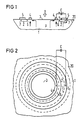
- FIGS. 1 and 2 A semiconductor body is shown in FIGS. 1 and 2, the base zone of which on the cathode side is designated by 1. For example, it is p-doped.
- An auxiliary emitter zone 2 is embedded in the surface of the base zone 1.
- the auxiliary emitter zone 2 is an annulus, which includes a light-sensitive area 3.
- the light-sensitive region is understood to mean that region which is intended for the incidence of light. The incident light is indicated by a thick arrow.
- the auxiliary emitter zone 2 has a pn junction, the inner edge of which is adjacent to the light-sensitive region 3 and is designated by 6. Its edge facing away from the light-sensitive area is designated by 7. Adjacent to the photosensitive region 3 there is a base electrode 4 on the base zone 1, which only contacts the base zone 1 and surrounds the photosensitive region 3.
- the base electrode 4 is, for example, also ring-shaped.
- the auxiliary emitter zone 2 is connected to an auxiliary emitter electrode 5, which is also ring-shaped.
- the auxiliary emitter electrode 5 contacts the auxiliary emitter zone 2 and the base zone 1 on the side facing the emitter zone 20 of the main thyristor.
- the outer edge 7 of the auxiliary emitter zone 2 is thus short-circuited.
- a capacitor C is connected between the electrodes 4 and 5. The capacitor therefore bridges the auxiliary emitter zone 2 in the direction from the photosensitive region 3 to the main emitter zone 20.
- a voltage current applied to the thyristor in the blocking direction generates a displacement current that comes from inside of the semiconductor body flows to the cathode side. This stream is symbolized by the thin upward arrows. A large part of this current flows through the electrode 4 into the capacitor C and charges it. A smaller part of the displacement current flows radially outwards under the auxiliary emitter zone 2 to the electrode 5. The current flowing to the electrode 5 biases the auxiliary emitter. Because a large part of the displacement current does not flow radially under the auxiliary emitter to the electrode 5 but instead into the capacitor, the displacement current, ie the du / dt at the thyristor, can be increased without the auxiliary thyristor igniting.
- SMD surface mounted device
- a typical area requirement of a capacitor of the above capacity is 2.0 x 1.2 mm2.
- the capacitor can also be integrated. can be applied, for example, with an oxide as a dielectric. In this case, the space requirement is greater.
- the capacitance of 8 nF it is around 0.2 cm2.
- FIGS. 3 and 4 An embodiment with a capacitor integrated on the thyristor is shown in FIGS. 3 and 4.
- the same or functionally identical parts as in FIGS. 1 and 2 have the same reference numerals.
- the base electrode 4 is connected to a conductor track 8, which is applied to an oxide layer 9 and lies in a gap in the auxiliary emitter electrode 5.
- the oxide layer 9, which can also be another insulating layer, insulates the conductor track 8 from the auxiliary emitter zone 2.
- the auxiliary emitter electrode 5 is connected to a contact finger 10, which is also on an insulating layer, e.g. an oxide layer 11 can be arranged.
- the mode of operation is the same as that mentioned in connection with FIGS. 1 and 2.
- the exemplary embodiments according to FIGS. 1 to 4 are characterized in that the light-sensitive area is the base zone 1 lying on the surface. However, as is known, the light-sensitive area can also be covered by the auxiliary emitter zone. Such an embodiment is shown in FIGS. 5 and 6.
- the auxiliary emitter zone is designated here by 14, the photosensitive region again by 3.
- the auxiliary emitter zone 14 is provided with an auxiliary emitter electrode 17 which also contacts the base zone 1.
- the base zone 1 is contacted with a base electrode 16 adjacent to the photosensitive region 3.
- the capacitor C is connected to the electrodes 16 and 17.
- a displacement current flowing out of the semiconductor body due to a du / dt load generates a current which is characterized by the thin, upward-pointing arrows. Most of the displacement current flows laterally under the emitter zone 14 or directly vertically to the electrode 16. The capacitor is thus charged in the specified polarity. A fraction of the displacement current flows laterally in the base zone below the auxiliary emitter zone 14 to the auxiliary emitter electrode 17 and from there to the main thyristor. Its path resistance is indicated by the dashed resistance symbol R.
- FIG. 6 5 is a section along the line V - V through FIG. 6.
- the auxiliary emitter zone 14 is provided with a strip-shaped extension 15 which extends radially to the zone 14.
- the length L of this extension determines the size of R for a given width.
- the extension is covered with a strip-shaped auxiliary emitter electrode 17. It also contacts the base zone 1 and lies opposite the emitter zone 20 of the main emitter.
- the base electrode 16 is also formed by a conductor strip which also extends essentially radially to the auxiliary emitter zone 14.
- the strips 16 and 17 are shaped such that an SMD capacitor can be mounted. However, they can also be shaped differently. Basically, the area of the strip 16 should be as small as possible.
- the contact 16 is surrounded by a trench 18.
- the trench 18 expediently also delimits the auxiliary emitter zone 14 and the long sides of the extension 15.
- the photo current generated under the zone 14 in the space charge zone is thus forced to flow under the extension 15.
- the trench can also extend to that side of the auxiliary emitter electrode which is opposite the base electrode 16.
- the photosensitivity is reduced until the capacitor C is charged. If it is charged, there is only the shunt caused by the auxiliary electrode between the auxiliary emitter zone 2 and the base zone 1.
Landscapes
- Physics & Mathematics (AREA)
- Condensed Matter Physics & Semiconductors (AREA)
- Electromagnetism (AREA)
- General Physics & Mathematics (AREA)
- Engineering & Computer Science (AREA)
- Computer Hardware Design (AREA)
- Microelectronics & Electronic Packaging (AREA)
- Power Engineering (AREA)
- Thyristors (AREA)
- Light Receiving Elements (AREA)
Description
Die Erfindung bezieht sich auf einen lichtsteuerbaren Thyristor mit einem Halbleiterkörper mit den Merkmalen
- a) der Halbleiterkörper hat einen lichtempfindlichen Bereich, eine Basiszone, eine Hilfsemitterzone und eine Hauptemitterzone,
- b) die Hilfsemitterzone ist mit einer Hilfsemitterelektrode kontaktiert,
- c) die Hilfsemitterelektrode kontaktiert einerseits die Hilfsemitterzone und andererseits die Basiszone auf der der Hauptemitterzone gegenüberliegenden Seite.
- a) the semiconductor body has a light-sensitive area, a base zone, an auxiliary emitter zone and a main emitter zone,
- b) the auxiliary emitter zone is contacted with an auxiliary emitter electrode,
- c) the auxiliary emitter electrode contacts on the one hand the auxiliary emitter zone and on the other hand the base zone on the side opposite the main emitter zone.
Ein solcher Thyristor ist z. B. in DE-A 27 15 482 oder in Patent Abstracts of Japan, Band 7, Nr. 72 (E-166)[1217], 25. März 1983 S. 127 E166 und JP-A-583 280 beschrieben worden. Die hauptsächlichen Anforderungen an einen lichtsteuerbaren Thyristor sind hohe Lichtempfindlichkeit bei gleichzeitig guter du/dt-Festigkeit. Die du/dt-Festigkeit wird im allgemeinen durch Emitter-Basisnebenschlüsse eingestellt. Bei durch Strom steuerbaren Thyristoren läßt sich diese Maßnahme sowohl beim Hilfsthyristor als auch beim Hauptthyristor anwenden.Such a thyristor is e.g. B. in DE-A 27 15 482 or in Patent Abstracts of Japan, Volume 7, No. 72 (E-166) [1217], March 25, 1983 p. 127 E166 and JP-A-583 280. The main requirements for a light-controllable thyristor are high light sensitivity with good du / dt strength. The dv / dt strength is generally set by emitter base shunts. In the case of current-controllable thyristors, this measure can be applied both to the auxiliary thyristor and to the main thyristor.
Bei durch Licht steuerbaren Thyristoren ist im allgemeinen die angebotene Lichtleistung sehr gering, so daß die Emitter-Basisnebenschlüsse im Hilfsthyristor sehr schwach angelegt werden müssen und die du/dt-Festigkeit dementsprechend gering ist.In the case of thyristors which can be controlled by light, the light output offered is generally very low, so that the emitter base shunts in the auxiliary thyristor must be applied very weakly and the du / dt strength is correspondingly low.
Ziel der Erfindung ist es, die du/dt-Festigkeit des Hilfsthyristors zu erhöhen, ohne die Lichtleistung wesentlich steigern zu müssen.The aim of the invention is to increase the du / dt strength of the auxiliary thyristor without having to significantly increase the light output.
Dieses Ziel wird gemäß einer ersten Alternative erreicht durch eine zwischen dem lichtempfindlichen Bereich und der Hilfsemitterzone angeordnete, die Basiszone kontaktierende Basiselektrode und durch einen Kondensator, der zwischen der Basiselektrode und der Hilfsemitterelektrode angeschlossen ist.According to a first alternative, this aim is achieved by a base electrode arranged between the light-sensitive region and the auxiliary emitter zone and contacting the base zone and by a capacitor connected between the base electrode and the auxiliary emitter electrode.
Gemäß einer zweiten Alternative wird dieses Ziel dadurch erreicht, daß der lichtempfindliche Bereich von der Hilfsemitterzone überdeckt ist, daß die Hilfsemitterelektrode und die Basiselektrode streifenförmig ausgebildet und bezüglich der Hilfsemitterzone radial angeordnet sind und daß der lichtempfindliche Bereich (3) von der Hilfsemitterzone (14) überdeckt ist, daß die Hilfsemitterelektrode (17) und die Basiselektrode streifenförmig ausgebildet und bezüglich der Hilfsemitterzone (14) radial angeordnet sind und daß ein Kondensator (c) zwischen der Basiselektrode und der Hilfsemitterelektrode angeschlossen ist.According to a second alternative, this object is achieved in that the light-sensitive area is covered by the auxiliary emitter zone, in that the auxiliary emitter electrode and the base electrode are strip-shaped and are arranged radially with respect to the auxiliary emitter zone and in that the light-sensitive area (3) is covered by the auxiliary emitter zone (14) is that the auxiliary emitter electrode (17) and the base electrode are strip-shaped and are arranged radially with respect to the auxiliary emitter zone (14) and that a capacitor (c) is connected between the base electrode and the auxiliary emitter electrode.
Die Erfindung wird anhand von Ausführungsbeispielen in Verbindung mit den Figuren 1 bis 6 näher erläutert. Es zeigen.
- Figur 1 und 2 den Schnitt und die Aufsicht auf ein erstes Ausführungsbeispiel,
Figur 3 und 4 den Schnitt und die Aufsicht auf ein zweites Ausführungsbeispiel,Figur 5 und 6 den Schnitt und die Aufsicht auf ein drittes Ausführungsbeispiel.
- 1 and 2 show the section and the supervision of a first embodiment,
- 3 and 4 the section and the supervision of a second embodiment,
- Figures 5 and 6 the section and the supervision of a third embodiment.
In den Figuren 1 und 2 ist ein Halbleiterkörper dargestellt, dessen katodenseitige Basiszone mit 1 bezeichnet ist. Sie ist beispielsweise p-dotiert. In die Oberfläche der Basiszone 1 ist eine Hilfsemitterzone 2 eingebettet. Die Hilfsemitterzone 2 ist ein Kreisring, der einen lichtempfindlichen Bereich 3 einschließt. Unter lichtempfindlichem Bereich wird bei diesem und den folgenden Ausführungsbeispielen derjenige Bereich verstanden, der zum Lichteinfall bestimmt ist. Das einfallende Licht ist durch einen dicken Pfeil gekennzeichnet.A semiconductor body is shown in FIGS. 1 and 2, the base zone of which on the cathode side is designated by 1. For example, it is p-doped. An
Die Hilfsemitterzone 2 hat einen pn-Übergang, dessen an den lichtempfindlichen Bereich 3 angrenzender Innenrand mit 6 bezeichnet ist. Sein vom lichtempfindlichen Bereich abgewandter Rand ist mit 7 bezeichnet. Angrenzend an den lichtempfindlichen Breich 3 liegt auf der Basiszone 1 eine Basiselektrode 4, die nur die Basiszone 1 kontaktiert und den lichtempfindlichen Bereich 3 umschließt. Die Basiselektrode 4 ist beispielsweise ebenfalls ringförmig aufgebildet. Die Hilfsemitterzone 2 ist mit einer Hilfsemitterelektrode 5 verbunden, die ebenfalls ringförmig ist. Die Hilfsemitterelektrode 5 kontaktiert die Hilfsemitterzone 2 und die Basiszone 1 auf der der Emitterzone 20 des Hauptthyristors zugewandten Seite. Der Außenrand 7 der Hilfsemitterzone 2 ist damit kurzgeschlossen. Zwischen den Elektroden 4 und 5 ist ein Kondensator C angeschlossen. Der Kondensator überbrückt also die Hilfsemitterzone 2 in Richtung vom lichtempfindlichen Bereich 3 zur Hauptemitterzone 20.The
Ein am Thyristor in Blockierrichtung anliegender Spannungsstrom erzeugt einen Verschiebungsstrom, der aus dem Inneren des Halbleiterkörpers zur Kathodenseite fließt. Dieser Strom ist durch die dünnen aufwärts gerichteten Pfeile symbolisiert. Ein großer Teil dieses Stroms fließt über die Elektrode 4 in den Kondensator C und lädt diesen auf. Ein geringerer Teil des Verschiebungsstroms fließt radial unter der Hilfsemitterzone 2 nach außen zur Elektrode 5 ab. Der zur Elektrode 5 abfließende Strom spannt den Hilfsemitter vor. Dadurch, daß ein großer Teil des Verschiebungsstroms nicht radial unter dem Hilfsemitter zur Elektrode 5 fließt sondern in den Kondensator, kann der Verschiebungsstrom, d.h. das du/dt am Thyristor erhöht werden, ohne daß der Hilfsthyristor zündet.A voltage current applied to the thyristor in the blocking direction generates a displacement current that comes from inside of the semiconductor body flows to the cathode side. This stream is symbolized by the thin upward arrows. A large part of this current flows through the
Eine Abschätzung der Größe des Kondensators C ergibt sich aus der Überlegung, daß die maximal verschiebbare Ladung pro Flächeneinheit im Halbleiterkörper des Thyristors bei 1,6 x 10⁻⁷ As/cm² entsprechend 10¹² Ladungsträger/cm² liegt. Die maximal mögliche Ladung pro Flächeneinheit ist dies deswegen, weil bei höherer Ladung die kritische Feldstärke erreicht und der Lawinendurchbruch einsetzen würde. Bei einem Radius des lichtempfindlichen Bereichs 3 von z.B. 0,7 mm ergibt sich damit eine Flächenladung von 2,5 x 10⁻⁹ As. Für die Kapazität ergibt sich, wenn der Kondensator auf 0,3 V aufgeladen werden soll somit
Der Kondensator C läßt sich am platzsparendsten in hybrider Form als auf einer Oberfläche montierbares Bauelement (SMD = surface mounted device) auf dem Halbleiterkörper des Thyristors aufbringen. Ein typischer Flächenbedarf eines Kondensators der obengenannten Kapazität ist 2,0 x 1,2 mm². Der Kondensator kann jedoch auch in integrierter Form. z.B. mit einem Oxid als Dielektrikum aufgebracht werden. In diesem Fall ist der Platzbedarf größer. Er liegt für die oben angegebene Kapazität von 8 nF bei rund 0,2 cm².The most space-saving capacitor C can be applied in a hybrid form as a surface-mountable device (SMD = surface mounted device) on the semiconductor body of the thyristor. A typical area requirement of a capacitor of the above capacity is 2.0 x 1.2 mm². However, the capacitor can also be integrated. can be applied, for example, with an oxide as a dielectric. In this case, the space requirement is greater. For the above-mentioned capacitance of 8 nF, it is around 0.2 cm².
Ein Ausführungsbeispiel mit einem auf dem Thyristor integrierten Kondensator ist in den FIG 3 und 4 angegeben. Hierbei haben gleiche oder funktionsgleiche Teile wie in den FIG 1 und 2 gleiche Bezugszeichen. Die Basiselektrode 4 ist mit einer Leiterbahn 8 verbunden, die auf einer Oxidschicht 9 aufgebracht ist und in einer Lücke der Hilfsemitterelektrode 5 liegt. Die Oxidschicht 9, die auch eine andere Isolierschicht sein kann, isoliert die Leiterbahn 8 gegen die Hilfsemitterzone 2. Die Hilfsemitterelektrode 5 ist mit einem Kontaktfinger 10 verbunden, der ebenfalls auf einer Isolierschicht, z.B. einer Oxidschicht 11 angeordnet sein kann. Die Wirkungsweise ist die gleiche wie die in Verbindung mit den FIG 1 und 2 erwähnte.An embodiment with a capacitor integrated on the thyristor is shown in FIGS. 3 and 4. The same or functionally identical parts as in FIGS. 1 and 2 have the same reference numerals. The
Die Ausführungsbeispiele nach den FIG 1 bis 4 sind dadurch charakterisiert, daß der lichtempfindliche Bereich die an der Oberfläche liegende Basiszone 1 ist. Der lichtempfindliche Bereich kann jedoch bekanntlich auch durch die Hilfsemitterzone abgedeckt sein. In FIG 5 und 6 ist ein solches Ausführungsbeispiel dargestellt. Die Hilfsemitterzone ist hier mit 14 bezeichnet, der lichtempfindliche Bereich wieder mit 3. Die Hilfsemitterzone 14 ist mit einer Hilfsemitterelektrode 17 versehen, die auch die Basiszone 1 kontaktiert. Die Basiszone 1 ist benachbart dem lichtempfindlichen Bereich 3 mit einer Basiselektrode 16 kontaktiert. An die Elektroden 16 und 17 ist der Kondensator C angeschlossen.The exemplary embodiments according to FIGS. 1 to 4 are characterized in that the light-sensitive area is the base zone 1 lying on the surface. However, as is known, the light-sensitive area can also be covered by the auxiliary emitter zone. Such an embodiment is shown in FIGS. 5 and 6. The auxiliary emitter zone is designated here by 14, the photosensitive region again by 3. The
Ein aus dem Halbleiterkörper aufgrund einer du/dt-Belastung fließender Verschiebungsstrom erzeugt einen Strom, der durch die dünnen, aufwärts gerichteten Pfeile charakterisiert ist. Der größte Teil des Verschiebungsstroms fließt lateral unter der Emitterzone 14 bzw. direkt vertikal zur Elektrode 16. Damit wird der Kondensator in der angegebenen Polarität aufgeladen. Ein Bruchteil des Verschiebungsstroms fließt in der Basiszone lateral unter der Hilfsemitterzone 14 zur Hilfsemitterelektrode 17 und von dort zum Hauptthyristor ab. Sein Bahnwiderstand ist durch das gestrichelte Widerstandssymbol R bezeichnet.A displacement current flowing out of the semiconductor body due to a du / dt load generates a current which is characterized by the thin, upward-pointing arrows. Most of the displacement current flows laterally under the
Eine günstige Ausführungsform ist in FIG 6 dargestellt. Die FIG 5 ist ein Schnitt entlang der Linie V - V durch die FIG 6. Die Hilfsemitterzone 14 ist mit einem streifenförmigen Fortsatz 15 versehen, der sich radial zur Zone 14 erstreckt. Die Länge L dieses Fortsatzes bestimmt bei gegebener Breite die Größe von R. Der Fortsatz ist mit einer streifenförmigen Hilfsemitterelektrode 17 bedeckt. Sie kontaktiert auch die Basiszone 1 und liegt der Emitterzone 20 des Hauptemitters gegenüber. Die Basiselektrode 16 wird ebenfalls durch einen Leiterstreifen gebildet, der sich im wesentlichen ebenfalls radial zur Hilfsemitterzone 14 erstreckt. Die Streifen 16 und 17 sind dabei derart geformt, daß sich ein SMD-Kondensator montieren läßt. Sie können jedoch auch anders geformt sein. Grundsätzlich sollte die Fläche des Streifens 16 so klein wie möglich sein.A favorable embodiment is shown in FIG. 6. 5 is a section along the line V - V through FIG. 6. The
Um sicherzustellen, daß der Verschiebungsstrom in den Kondensator fließt und nicht entlang der relativ hoch dotierten Oberfläche der Basiszone 1 zur Hilfsemitterelektrode abfließt, ist der Kontakt 16 von einem Graben 18 umgeben. Der Graben 18 begrenzt zweckmäßigerweise auch die Hilfsemitterzone 14 und die Längsseiten des Fortsatzes 15. Damit wird der unter der Zone 14 in der Raumladungszone erzeugte Fotostrom gezwungen, unter dem Fortsatz 15 zu fließen. Dort findet er einen relativ hohen Bahnwiderstand R vor. Dadurch erzeugt auch ein kleiner Fotostrom den zum Zünden notwendigen Spannungsabfall von etwa 0,5 V. Der Graben kann sich auch auf diejenige Seite der Hilfsemitterelektrode erstrecken, die der Basiselektrode 16 gegenüberliegt.To ensure that the displacement current flows into the capacitor and does not flow along the relatively highly doped surface of the base zone 1 to the auxiliary emitter electrode, the
Für alle Ausführungsbeispiele gilt, daß die Lichtempfindlichkeit so lange herabgesetzt ist, bis der Kondensator C aufgeladen ist. Ist er aufgeladen, so besteht nur noch der durch die Hilfselektrode bewirkte Nebenschluß zwischen der Hilfsemitterzone 2 und der Basiszone 1.For all exemplary embodiments, the photosensitivity is reduced until the capacitor C is charged. If it is charged, there is only the shunt caused by the auxiliary electrode between the
Claims (7)
- Light-controllable thyristor having a semiconductor body with the features:a) the semiconductor body has a photosensitive area (3), a base zone (1), an auxiliary emitter zone (2; 14) and a main emitter zone (20),b) the auxiliary emitter zone is in contact with an auxiliary emitter electrode (5; 17),c) the auxiliary emitter electrode (5; 17) is in contact, on the one hand, with the auxiliary emitter zone (2) and, on the other hand, the base zone (1) on the side situated opposite the main emitter zone (20),characterised by a base electrode (4) disposed between the photosensitive area (3) and the auxiliary emitter zone (2) and in contact with the base zone (1), and by a capacitor (C) connected between the base electrode (4) and the auxiliary emitter electrode.
- Light-controllable thyristor according to Claim 1, characterised in that the base electrode (4) and the auxiliary emitter zone (2) are of annular construction and surround the photosensitive area (3).
- Light-controllable thyristor having a semiconductor body with the features:a) the semiconductor body has a photosensitive area (3), a base zone (1), an auxiliary emitter zone (2; 14) and a main emitter zone (20),b) the auxiliary emitter zone is in contact with an auxiliary emitter electrode (5; 17),c) the auxiliary emitter electrode (5; 17) is in contact, on the one hand, with the auxiliary emitter zone (2) and, on the other hand, with the base zone (1) on the side situated opposite the main emitter zone (20),characterised in that the photosensitive area (3) is covered by the auxiliary emitter zone (14), in that the auxiliary emitter electrode (17) and the base electrode are of strip-type construction and are disposed radially with respect to the auxiliary emitter zone (14), and in that a capacitor (C) is connected between the base electrode and the auxiliary emitter electrode.
- Thyristor according to Claim 3, characterised in that the auxiliary emitter zone (14) has a strip-type extension (15), and in that the auxiliary emitter zone, the base electrode (16) and both long sides of the extension are surrounded by a trench (18) situated in the base zone (1) and deeper than the auxiliary emitter zone.
- Thyristor according to one of Claims 1 to 5, characterised in that the capacitor (C) is mounted on the semiconductor body.
- Thyristor according to Claim 5, characterised in that the capacitor (C) is a surface-mountable component and is mounted directly on the auxiliary emitter electrode (17) and the base electrode (16) by means of its connections.
- Thyristor according to Claim 5, characterised in that the capacitor (C) is disposed in integrated form on the surface of the semiconductor body.
Applications Claiming Priority (2)
| Application Number | Priority Date | Filing Date | Title |
|---|---|---|---|
| DE3727820 | 1987-08-20 | ||
| DE3727820 | 1987-08-20 |
Publications (2)
| Publication Number | Publication Date |
|---|---|
| EP0304032A1 EP0304032A1 (en) | 1989-02-22 |
| EP0304032B1 true EP0304032B1 (en) | 1993-01-27 |
Family
ID=6334143
Family Applications (1)
| Application Number | Title | Priority Date | Filing Date |
|---|---|---|---|
| EP88113350A Expired - Lifetime EP0304032B1 (en) | 1987-08-20 | 1988-08-17 | Light controlled thyristor |
Country Status (3)
| Country | Link |
|---|---|
| EP (1) | EP0304032B1 (en) |
| JP (1) | JPH01120063A (en) |
| DE (1) | DE3877858D1 (en) |
Families Citing this family (1)
| Publication number | Priority date | Publication date | Assignee | Title |
|---|---|---|---|---|
| JP4175379B2 (en) | 2006-04-25 | 2008-11-05 | 日本電気株式会社 | File sharing method and file sharing system |
Family Cites Families (4)
| Publication number | Priority date | Publication date | Assignee | Title |
|---|---|---|---|---|
| DE2458401C2 (en) * | 1974-12-10 | 1982-06-24 | Siemens AG, 1000 Berlin und 8000 München | Thyristor controllable with light |
| DE2538549C2 (en) * | 1975-08-29 | 1985-06-13 | Siemens AG, 1000 Berlin und 8000 München | Thyristor controllable with light |
| DE2715482C2 (en) * | 1977-04-06 | 1985-06-13 | Siemens AG, 1000 Berlin und 8000 München | Thyristor controllable with light |
| US4489340A (en) * | 1980-02-04 | 1984-12-18 | Nippon Telegraph & Telephone Public Corporation | PNPN Light sensitive semiconductor switch with phototransistor connected across inner base regions |
-
1988
- 1988-08-17 DE DE8888113350T patent/DE3877858D1/en not_active Expired - Fee Related
- 1988-08-17 EP EP88113350A patent/EP0304032B1/en not_active Expired - Lifetime
- 1988-08-19 JP JP63206220A patent/JPH01120063A/en active Pending
Also Published As
| Publication number | Publication date |
|---|---|
| JPH01120063A (en) | 1989-05-12 |
| DE3877858D1 (en) | 1993-03-11 |
| EP0304032A1 (en) | 1989-02-22 |
Similar Documents
| Publication | Publication Date | Title |
|---|---|---|
| DE2625917A1 (en) | SEMI-CONDUCTOR ARRANGEMENT | |
| DE2932152A1 (en) | OVERVOLTAGE PROTECTION FOR THE PROTECTION OF UNITS THAT CONTAIN SEMICONDUCTOR ELEMENTS FOR SMALL PERFORMANCE | |
| DE19653615A1 (en) | Power semiconductor device fabricating method | |
| CH668505A5 (en) | SEMICONDUCTOR COMPONENT. | |
| EP0039943B1 (en) | Thyristor having controllable emitter shorts and process for its operation | |
| DE2716874C2 (en) | Thyristor | |
| DE3521079C2 (en) | ||
| DE3631136C2 (en) | ||
| DE3401407C2 (en) | ||
| DE2922301C2 (en) | Light controllable thyristor and method for its manufacture | |
| DE3102851C2 (en) | PNPN semiconductor switch | |
| EP0014435B1 (en) | Thyristor controlled by field effect transistor | |
| DE1216435B (en) | Switchable semiconductor component with four zones | |
| DE4022022A1 (en) | HIGH VOLTAGE SEMICONDUCTOR DEVICE | |
| EP0430133B1 (en) | Power semiconductor device having emitter shorts | |
| DE3502180A1 (en) | SOLID RELAY | |
| DE2915885C2 (en) | Thyristor controlled by field effect transistor | |
| EP0304032B1 (en) | Light controlled thyristor | |
| DE2329398B2 (en) | Thyristor component conducting in the reverse direction | |
| EP0559945B1 (en) | Turn-off power semi-conductor device | |
| DE2425364A1 (en) | GATE-CONTROLLED SEMI-CONDUCTOR RECTIFIER | |
| DE4439012A1 (en) | Bidirectional thyristor for high voltage blocking | |
| DE1210490B (en) | Controllable semiconductor component with a pnpn or npnp zone sequence and method for manufacturing | |
| DE2346256C3 (en) | Thyristor | |
| DE2449089C3 (en) | Controllable semiconductor rectifier |
Legal Events
| Date | Code | Title | Description |
|---|---|---|---|
| PUAI | Public reference made under article 153(3) epc to a published international application that has entered the european phase |
Free format text: ORIGINAL CODE: 0009012 |
|
| AK | Designated contracting states |
Kind code of ref document: A1 Designated state(s): CH DE FR GB LI SE |
|
| 17P | Request for examination filed |
Effective date: 19890726 |
|
| 17Q | First examination report despatched |
Effective date: 19910411 |
|
| GRAA | (expected) grant |
Free format text: ORIGINAL CODE: 0009210 |
|
| AK | Designated contracting states |
Kind code of ref document: B1 Designated state(s): CH DE FR GB LI SE |
|
| REF | Corresponds to: |
Ref document number: 3877858 Country of ref document: DE Date of ref document: 19930311 |
|
| ET | Fr: translation filed | ||
| GBT | Gb: translation of ep patent filed (gb section 77(6)(a)/1977) |
Effective date: 19930401 |
|
| PGFP | Annual fee paid to national office [announced via postgrant information from national office to epo] |
Ref country code: GB Payment date: 19930714 Year of fee payment: 6 |
|
| PGFP | Annual fee paid to national office [announced via postgrant information from national office to epo] |
Ref country code: SE Payment date: 19930813 Year of fee payment: 6 |
|
| PGFP | Annual fee paid to national office [announced via postgrant information from national office to epo] |
Ref country code: FR Payment date: 19930819 Year of fee payment: 6 |
|
| PGFP | Annual fee paid to national office [announced via postgrant information from national office to epo] |
Ref country code: DE Payment date: 19931020 Year of fee payment: 6 |
|
| PGFP | Annual fee paid to national office [announced via postgrant information from national office to epo] |
Ref country code: CH Payment date: 19931116 Year of fee payment: 6 |
|
| PLBE | No opposition filed within time limit |
Free format text: ORIGINAL CODE: 0009261 |
|
| STAA | Information on the status of an ep patent application or granted ep patent |
Free format text: STATUS: NO OPPOSITION FILED WITHIN TIME LIMIT |
|
| 26N | No opposition filed | ||
| PG25 | Lapsed in a contracting state [announced via postgrant information from national office to epo] |
Ref country code: GB Effective date: 19940817 |
|
| PG25 | Lapsed in a contracting state [announced via postgrant information from national office to epo] |
Ref country code: SE Effective date: 19940818 |
|
| PG25 | Lapsed in a contracting state [announced via postgrant information from national office to epo] |
Ref country code: LI Effective date: 19940831 Ref country code: CH Effective date: 19940831 |
|
| EAL | Se: european patent in force in sweden |
Ref document number: 88113350.8 |
|
| GBPC | Gb: european patent ceased through non-payment of renewal fee |
Effective date: 19940817 |
|
| PG25 | Lapsed in a contracting state [announced via postgrant information from national office to epo] |
Ref country code: FR Effective date: 19950428 |
|
| REG | Reference to a national code |
Ref country code: CH Ref legal event code: PL |
|
| PG25 | Lapsed in a contracting state [announced via postgrant information from national office to epo] |
Ref country code: DE Effective date: 19950503 |
|
| EUG | Se: european patent has lapsed |
Ref document number: 88113350.8 |
|
| REG | Reference to a national code |
Ref country code: FR Ref legal event code: ST |