EP0303230B1 - PCM signal reproducing/recording apparatus - Google Patents
PCM signal reproducing/recording apparatus Download PDFInfo
- Publication number
- EP0303230B1 EP0303230B1 EP88112939A EP88112939A EP0303230B1 EP 0303230 B1 EP0303230 B1 EP 0303230B1 EP 88112939 A EP88112939 A EP 88112939A EP 88112939 A EP88112939 A EP 88112939A EP 0303230 B1 EP0303230 B1 EP 0303230B1
- Authority
- EP
- European Patent Office
- Prior art keywords
- data
- sub
- code
- code data
- pcm
- Prior art date
- Legal status (The legal status is an assumption and is not a legal conclusion. Google has not performed a legal analysis and makes no representation as to the accuracy of the status listed.)
- Expired - Lifetime
Links
- 238000001514 detection method Methods 0.000 claims description 42
- 230000005540 biological transmission Effects 0.000 claims description 11
- 238000010586 diagram Methods 0.000 description 7
- 230000006870 function Effects 0.000 description 5
- 238000006243 chemical reaction Methods 0.000 description 3
- 230000005236 sound signal Effects 0.000 description 2
- 239000013078 crystal Substances 0.000 description 1
- 238000013500 data storage Methods 0.000 description 1
- 230000004048 modification Effects 0.000 description 1
- 238000012986 modification Methods 0.000 description 1
Images


Classifications
-
- G—PHYSICS
- G11—INFORMATION STORAGE
- G11B—INFORMATION STORAGE BASED ON RELATIVE MOVEMENT BETWEEN RECORD CARRIER AND TRANSDUCER
- G11B27/00—Editing; Indexing; Addressing; Timing or synchronising; Monitoring; Measuring tape travel
- G11B27/10—Indexing; Addressing; Timing or synchronising; Measuring tape travel
- G11B27/19—Indexing; Addressing; Timing or synchronising; Measuring tape travel by using information detectable on the record carrier
- G11B27/28—Indexing; Addressing; Timing or synchronising; Measuring tape travel by using information detectable on the record carrier by using information signals recorded by the same method as the main recording
- G11B27/30—Indexing; Addressing; Timing or synchronising; Measuring tape travel by using information detectable on the record carrier by using information signals recorded by the same method as the main recording on the same track as the main recording
- G11B27/3027—Indexing; Addressing; Timing or synchronising; Measuring tape travel by using information detectable on the record carrier by using information signals recorded by the same method as the main recording on the same track as the main recording used signal is digitally coded
- G11B27/3063—Subcodes
-
- G—PHYSICS
- G11—INFORMATION STORAGE
- G11B—INFORMATION STORAGE BASED ON RELATIVE MOVEMENT BETWEEN RECORD CARRIER AND TRANSDUCER
- G11B20/00—Signal processing not specific to the method of recording or reproducing; Circuits therefor
- G11B20/10—Digital recording or reproducing
- G11B20/10527—Audio or video recording; Data buffering arrangements
-
- G—PHYSICS
- G11—INFORMATION STORAGE
- G11B—INFORMATION STORAGE BASED ON RELATIVE MOVEMENT BETWEEN RECORD CARRIER AND TRANSDUCER
- G11B27/00—Editing; Indexing; Addressing; Timing or synchronising; Monitoring; Measuring tape travel
- G11B27/02—Editing, e.g. varying the order of information signals recorded on, or reproduced from, record carriers
- G11B27/031—Electronic editing of digitised analogue information signals, e.g. audio or video signals
- G11B27/032—Electronic editing of digitised analogue information signals, e.g. audio or video signals on tapes
-
- G—PHYSICS
- G11—INFORMATION STORAGE
- G11B—INFORMATION STORAGE BASED ON RELATIVE MOVEMENT BETWEEN RECORD CARRIER AND TRANSDUCER
- G11B27/00—Editing; Indexing; Addressing; Timing or synchronising; Monitoring; Measuring tape travel
- G11B27/10—Indexing; Addressing; Timing or synchronising; Measuring tape travel
- G11B27/19—Indexing; Addressing; Timing or synchronising; Measuring tape travel by using information detectable on the record carrier
- G11B27/28—Indexing; Addressing; Timing or synchronising; Measuring tape travel by using information detectable on the record carrier by using information signals recorded by the same method as the main recording
- G11B27/30—Indexing; Addressing; Timing or synchronising; Measuring tape travel by using information detectable on the record carrier by using information signals recorded by the same method as the main recording on the same track as the main recording
- G11B27/3027—Indexing; Addressing; Timing or synchronising; Measuring tape travel by using information detectable on the record carrier by using information signals recorded by the same method as the main recording on the same track as the main recording used signal is digitally coded
-
- G—PHYSICS
- G11—INFORMATION STORAGE
- G11B—INFORMATION STORAGE BASED ON RELATIVE MOVEMENT BETWEEN RECORD CARRIER AND TRANSDUCER
- G11B2220/00—Record carriers by type
- G11B2220/90—Tape-like record carriers
-
- G—PHYSICS
- G11—INFORMATION STORAGE
- G11B—INFORMATION STORAGE BASED ON RELATIVE MOVEMENT BETWEEN RECORD CARRIER AND TRANSDUCER
- G11B2220/00—Record carriers by type
- G11B2220/90—Tape-like record carriers
- G11B2220/91—Helical scan format, wherein tracks are slightly tilted with respect to tape direction, e.g. VHS, DAT, DVC, AIT or exabyte
- G11B2220/913—Digital audio tape [DAT] format
Definitions
- the present invention relates to a system for reproducing PCM data and sub-code data from a first recording medium and recording the PCM data and sub-code data onto a second recording medium according to claim 1, to a PCM signal reproducing apparatus for reproducing PCM data and sub-code data according to claim 3 and to a PCM signal recording apparatus for recording PCM data and sub-code data according to claim 6.
- European Patent Application EP-A-0 209 141 on which the preamble of claim 1 is based discloses a PCM signal recording and reproducing apparatus, in which two memory circuits (RAMs) are provided. While PCM signals are read and written using one of the two memory circuits, PCM signals stored in the other memory circuit are error-corrected. At the end of writing with respect to the former memory circuit, the two memory circuits are interchanged to read the error-corrected PCM signals stored in the latter memory circuit. The read-out error-corrected PCM signals are then recorded on another magnetic tape, thus dispensing with a parity adding circuit necessary for recording and realizing inexpensive copying.
- PCM data main data
- sub-code data including sub-data and sub-ID for adding auxiliary information to the PCM data are recorded on a magnetic tape.
- the sub-code data is for recording information such as order and time of the PCM data and has information of 64 bites per set. Eight sets of the same information are recorded on one track on a tape.
- the whole of the data reproduced by the reproducing device is transmitted to the recording device so as to be recorded as it is.
- the recording device has no function to record the raw reproduced-data as it is, and therefore it is necessary that the recording device is additionally provided with a function to extract a necessary part, that is, the PCM data and sub-code data, from the received raw reproduced data to thereby reconstruct recording data.
- a function is the same as that in the reproducing device to extract the PCM data and sub-code data from the data reproduced by the reproducing device. Accordingly, provision of such a function in the recording device means that the same function is provided wastefully in each of the reproducing device and the recording device.
- a system combining a PCM signal reproducing apparatus and a PCM signal recording apparatus is provided as a system for reproducing PCM data and sub-code data from a first recording medium and recording the PCM data and sub-code data onto a second recording medium, said sub-code data having sub-data for adding auxiliary information to said PCM data, said sub-code data and said PCM data being recorded on said first and on said second recording medium in a frame format together with error detection codes for the PCM data as well as for the sub-code data, said system comprising a reproducing device for reproducing said data from the first recording medium, a recording device for recording said data on the second recording medium and transmission means for transmitting said data from the reproducing device to the recording device, in which said reproducing device includes means for reproducing said data, means for de-formatting the data reproduced and means for detecting errors in the sub-code data, and
- This system combines the advantages of the PCM signal reproducing apparatus and the PCM signal recording apparatus. These advantages will be described in connection with the reproducing apparatus and the recording apparatus.
- the PCM signal reproducing/recording apparatus for reproducing PCM data and sub-code data is arranged so that said sub-code data having sub-data for adding auxiliary information to said PCM data, said sub-code data and said PCM data being recorded on a medium together with error detection codes for the PCM data as well as for the sub-code data, said apparatus comprising a reproducing device for reproducing said data from said recording medium, in which said reproducing device includes means for reproducing said data, means for detecting errors in the sub-code data, means responsive to said error detection means for generating validity flags indicating the correctness of incorrectness of the sub-code data, means for formatting the PCM data, the sub-code data and the corresponding validity flags in a sub-frame comprising, a sub-code portion, a PCM data portion and said flags and means for outputting the said sub-frames. Only a minimum number of signal lines for transmission is required.
- the PCM signal recording apparatus for recording PCM data and sub-code data, said sub-code data having sub-data for adding auxiliary information to said PCM data, according to the present invention es arranged so that said sub-code data and said PCM data being reproduced from a medium which is recorded in a frame format together with error detection codes for the PCM data as well as for the sub-code data, in each said frame sub-code data related to the same PCM data is repeated a plurality of times
- said apparatus comprising a recording device for recording said data on the said recording medium, in which said recording device includes means for receiving reproduced sub-code data and validity flags indicating the correctness or incorrectness of each of said plurality of sub-code data in said frame, means for supplying error detection codes related to said sub-code data, means for formatting said sub-code data and said error detection codes in said frame format, means for recording said formatted data, and said recording device including means for selecting a correct one out of said plurality of sub-code data on the basis of the said received validity flags, and
- the arrangement of the sub-code data is performed by the frame of the reproduced data, it is possible to make simple the operation of the recording device in which the transmitted sub-code data is received and processed to obtain a magnetic tape having the same contents as that of the reproduced magnetic tape.
- the sub-ID has program NO and control ID and the program NO and control ID are transmitted only once in one frame of the reproduced data, the task for receiving and processing the sub-data is reduced correspondingly and efficiently.
- the sub-data recording can be performed with high reliability in the recording device in which the data is received.
- the recording apparatus when the sub-code data is read out from a RAM so as to be recorded on a magnetic tape, only the data in the sub-code write region is made access repeatedly eight times by a record data address generation circuit so that eight sets of one and the same valid sub-code data are multiplex-recorded on the tape to thereby prevent recording of erroneous data.
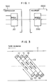
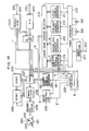
- Fig. 1 shows that the PCM signal reproducing/recording apparatus according to the present invention is constituted by a reproducing device 500 including at least a modulation circuit 20, and a recording device 1500 including at least a demodulation circuit 300.
- Fig. 2 is a block diagram showing the reproducing device of the PCM signal reproducing/recording apparatus according to the present invention.
- the arrangement includes: a magnetic tape 11 on which main data of PCM audio data, and sub-data, etc., are recorded; a rotary drum 12 having a pair of heads 121 and 122; a reproduction amplifier 13; a demodulation circuit 14; a memory (RAM) 16; an error correction circuit (ECU) 17; and an address control circuit 18.
- the magnetic tape 11 has a recording format thereon as shown in Fig. 3.
- the magnetic tape 11 has sub-data area 111 and 112 in which sub-data is recorded and a main data area 113 in which main data composed of PCM audio data is recorded.
- the sub-data areas 111 and 112 8 blocks per track, that is, 16 blocks in total, of the sub-data is recorded in each of the sub-data areas 111 and 112, while 128 blocks of main data is recorded in the main data area 113.
- each of the 16 sub-data blocks forming each of the sub-data areas 111 and 112 is composed of sync.
- sub-ID SW1 and SW2
- sub-ID parity sub-data
- sub-data sub-data
- the sync is formed on one symbol
- the sub-ID parity is formed on one symbol
- the sub-data is composed of 32 symbols.
- One sub-data block has sub-data of 32 symbols, and the sub-data blocks include two kinds of blocks, one including only data, the other including not only data but parity.
- the respective symbols have numbers 0 ... 31 in the order along the direction of record.
- the sub-data is composed of data (SD 0,0 - SD 15,23 ) and parity (SP 1,24 - SP 15,31 ) and the sub-data per track has data of 448 symbols and parity of 64 symbols.
- the parity is used as a code for data error detection and correction.
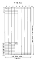
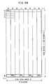
- the positioning of the sub-data is as shown in Fig. 5.
- Pack ID shows the number of packs included in the sub-data in two blocks starting from an even-numbered block.
- the sub-data is composed of only packs, and the maximum capacity of the sub-data is 7 packs per two blocks. The number of packs used actually is indicated by the pack ID and all the remainder of the pack area of the sub-data is made to be "0".
- the pack ID of SW2 indicates the number of packs in the sub-data, and the pack areas 1 - 7 are arranged as shown in Fig. 6.
- the pack data is successively recorded in accordance with the area number.
- the aforementioned data recorded on the magnetic tape 11 is reproduced by the pair of heads 121 and 122 provided on the rotary drum 12. After amplified by the reproduction amplifier 13, the reproduced data is demodulated by the 10-8 demodulation circuit 14. The demodulated data is applied to the memory 16 through a data bus 15.
- the error correction circuit 17 corrects an error in the data by use of the parity (correction code) contained in the data and causes the memory 16 to store C1 correction flag indicating the state of error.
- the address control circuit 18 generates a predetermined address signal in synchronism with a predetermined timing signal generated by a not-shown decoder on the basis of a data selection signal.
- the address signal is applied to the memory 16 through an address bus 19 so that the data stored in the address of the memory 16 designated by the address signal is read out through the data bus 15.
- the main data and C1 correction flag read out from the memory 16 are supplied to the interface modulation circuit 20.
- the respective outputs from a frame sync generation circuit 21, a preamble generation circuit 22, a sub-ID detection circuit 23, a sub-data generation circuit 24, and a main data ID detection circuit 25 are supplied to the interface modulation circuit 20, and then, after biphase-modulated in the interface modulation circuit 20, supplied to the recording device 1500 shown in Fig. 14.
- Fig. 7 shows a format of a signal transmitted from the modulation circuit 20 to the recording device shown in Fig. 14.
- the format is composed of 192 frames and each frame is composed of two sub-frames.
- the format of each sub-frame is composed of a preamble portion to which 4 time slots are allotted, an AUX-DATA portion to which 8 time slots are allotted, a PCM data portion to which 16 time slots are allotted, and a remainder portion of 4 times slots, as shown in Fig. 8.
- each sub-frame is composed of 32 time slots.
- the remainder portion of 4 times slots has a validity indicating bit V, a user's bit U, a channel status bit C, and a parity bit P. the validity indicating bit V, the user's bit U, and the channel status bit C are used by the 192 frames.
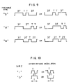
- the preamble portion three kinds of patterns B, W and M are included.
- the pattern B is added to the CH1 at the head of a block
- the pattern M is added to the CH1 other than the CH1 at the head of a block
- the pattern W is added to the head of each of the sub-frames CH2, CH3, 07.
- Those patterns B, W and M have such specific patterns as shown in Fig. 9.
- the "1" and "0" of NRZ are modulated into biphase patterns with T and 2T as shown in Fig. 10.
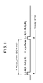
- Fig. 11 shows the signal format at that time.
- main data L0 is allotted to the PCM data portion
- program NO1 of the sub-ID and control ID are allotted to the AUX-DATA portion, in the first sub-frame
- main data R0 is allotted to the PCM data portion
- program NO2 and program NO3 of the sub-ID are allotted to the AUX-DATA portion, in the next sub-frame.
- L1, R1, L2, and R2 are allotted to the PCM data portion and nothing is allotted to the AUX-DATA portion.
- L3 is allotted to the PCM data portion and pack ID of the sub-ID and Data ID are allotted to the AUX-DATA portion in the first sub-frame, and R3 is allotted to the PCM data portion and a C1 flag is allotted to the AUX-DATA portion in the next sub-frame.
- main data L4, .., L31, R4, ..., R31 are allotted to the respective PCM portions and packs 1, 3, 5, 7, 2, 4, 6 of sub-data are allotted in order to the AUX-DATA portions.
- transmission of sub-ID and sub-data for two blocks has been completed.
- transmission of sub-data for the next two blocks is performed from the 33rd frame.
- the program NO and control ID of sub-ID are not transmitted but only the remainder of the sub-ID and sub-data are transmitted as shown in Fig. 13.
- Fig. 13 shows the sub-ID and sub-data in AUX-DATA portions transmitted in one revolution of the rotary drum, that is, in one frame of reproduced data. Since the control ID of the sub-ID does not change during one frame, only once transmission of the control ID sufficies so that the burden on the transmission side as well as the reception side can be reduced.
- the frame sync. generation circuit 21 generates frame sync. in synchronism with the rotation of the rotary drum 12 and the preamble generation circuit 22 generates one of the three kinds of patterns at the head of each sub-frame on the basis of the sync., the pattern being supplied to the modulation circuit 20.
- the sub-ID detection circuit 23 supplies various ID data of the detected sub-ID to the modulation circuit 20 at predetermined timing at the head of one revolution of the rotary drum and the head of every two blocks of the sub-data.
- the sub-data generation circuit 24 generates sub-data, that is, pack data 1-7 at predetermined timing on the basis of the data read out from the memory 16 and supplies the thus generated sub-data to the modulation circuit 20.
- the main data ID detection circuit 25 detects various data on the basis of the data read out from the memory 16 and supplies the detected data to modulation circuit 20 for providing V, U, C and P.
- the modulation circuit 20 biphase-modulates the main data which has been read-out from the memory 16 and supplied thereto, and supplies the biphase-modulated main data to the recording device 1500.
- Fig. 14 is a block diagram of the recording device 1500 of the PCM signal reproducing/recording apparatus.
- the recording device 1500 is provided with a demodulation circuit 300 for demodulating the PCM data (main data) and sub-code data (sub-data, sub-ID, etc.) received from the modulation circuit 20 through a data input terminal 301 and for generating a sub-code input command 1; an A/D conversion circuit 200 for converting an analog signal into a PCM signal; a magnetic tape 221; a rotary cylinder 200; heads 222 and 223; a recording circuit 209 constituted by a recording amplifier and so on; a modulation circuit 208; a RAM 207 which is a storage circuit for temporarily storing data and which has a capacity of 256 Kbits; a coding circuit 205 for generating parity; a reset circuit 206 for zero-resetting the input data to the RAM 207; a write control circuit 219 for sending a write command to the RAM 207; a higher-rank address generation circuit 218 for controlling the higher-rank three bits of the address of the RAM 207; a coding address generation circuit
- An analog signal is supplied through the audio signal input terminal and converted into a PCM signal by the A/D conversion circuit 200.
- the thus converted PCM signal is stored in the RAM 207 at the address controlled by the PCM data address generation circuit 212.
- Data is read out from the RAM 207 with the address controlled by the coding address generation circuit 211, and parity is generated by the coding circuit 205 and written into the RAM 207.
- data is read out from the RAM 207, modulated in the modulation circuit 208, amplified in the recording circuit 209, and recorded on the magnetic tape 221 by the heads 222 and 223.
- the PCM data is supplied from the demodulation circuit 300, stored in the RAM 207 with the address controlled by the sub-code input address generation circuit 214, subject to the same processing as above, and recorded on the magnetic tape 221.
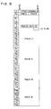
- Fig. 15 is an RAM map showing the region where those sub-code data 34 and C1 parity 35 are stored.
- Fig. 15 shows the data storage region of one track and this one face is a capacity of one track.
- the sub-code is stored in the central region indicated by a thick solid line 46. In this region, data is stored in the vertical direction along the direction of recording on the tape. This region is composed of 512 bites arranged in four columns. In Fig. 15, the coordinates represent the address of the RAM 207 with hexadecimal notation.
- the region 34 is used also as a region for the C2 parity for the PCM data, and in the actual case of write, after PCM data has been written on the magnetic tape 221 succeeding PCM data is inputted and written in the interval before parity is generated.
- a hatched region 47 is called a sub-code write-in region which will be described later.
- Sub-code input command 1 is supplied from the demodulation circuit 300 and sub-code data is also inputted from the demodulation circuit 300 in synchronism with the sub-code input command 1.
- the sub-code input address generation circuit 214 detects the timing of input of the ID data and flag data and sends detection commands 4 and 5 to the validity detection circuit 233 which checks whether all the check bit, data ID and C1 flag are "0" or not.
- the validity detection circuit 233 sends a "0" detection signal 2 to the write control circuit 219 which transfers a write command 3 to the RAM 207 so that the RAM 207 stores the sub-code data.
- the sub-code input address generation circuit 214 makes access only to a specific region composed of 64 bites so that write is made at a specific address independently of the position of valid sub-code data.
- the region is called a sub-code write-in region.
- the validity detection circuit 233 Upon detection of completion of transfer of the sub-code data of two tracks (64 bites) by the sub-code input address generation circuit 214, the validity detection circuit 233 is controlled to stop the "0" detection signal 2 so as to reset the write command 3 to thereby terminate the storing operation into the RAM 207.
- the validity detection circuit 233 Upon completion of input of the sub-code data of two tracks (1024 bites), the validity detection circuit 233 returns into a reset state and then performs validity detection.
- the recording data address generation circuit 213 is caused to repeatedly make access only to the sub-code write-in region 47 so that the sub-code data is read out from the region 47 and recorded in the sub-code recording area on the tape.
- valid data can be recorded in octuple on the tape.
- the recording device 1500 it is possible to prevent recording of sub-code data having errors and sub-code data having a format other than a specified one.
- Fig. 16 shows an example of the sub-code input address generation circuit 214 and the validity detection circuit 233.
- the sub-code input address generation circuit 214 includes a counter 70 and a timing decoding circuit 71 for deriving a necessary timing from the counter 70
- the validity detection circuit 233 includes latches 72 - 75, OR circuits 76 - 78, an AND circuit 79, NAND circuits 80 - 83, and inverters 84 - 88.
- the reference numeral 5 represents a clear signal.
- Each of the counter 70, and the latch circuits 72 - 75 is actuated to operate at a trailing edge of a clock.
- the reset of the latch circuits 74 and 75 is actuated by a high level and the set of the latch circuit 75 is actuated by a low level.
- the Q-output signal 113 of the latch circuit 75 is inverted by the inverter 88 so that the sub-code input command 1 is gated by the AND circuit 79 and transferred as the "0" detection signal 2 into the write control circuit 219. Accordingly, control is made so that the input sub-code data is written into the RAM 207 when the signal 113 is in low level while the write is inhibited when the signal 113 is in high level.
- the reference numerals 5 and 4 represent a latch clock for ID data check and a latch clock for flag data check.
- LSB and MSB labeled at the input sub-code data 6 represent the least significant bit and the most significant bit respectively.
- Fig. 17 shows the operation in the case where only the third set of ID data and flag data are indicated to be valid (hatched data).
- the latch circuits 75 and 74 are reset because the signal 101 is high, the signals 106 and 113 become low, and the input sub-code data 6 is written in the RAM 207.
- the high level is latched by the latch circuit 72 or 73, the output 104 of the OR circuit 78 is made high, and the output 115 of the inverter 87 is made low, so that the output 108 of the NAND circuit 84 becomes high. Accordingly, the high level is latched by the latch circuit 75 at a trailing edge 91 of a signal 109, and the signal 113 becomes high to thereby inhibit write of the RAM (hereinafter referred to as "RAM write").
- the output 105 of the NAND circuit 82 is low, so that the signal 106 is left as it is in low level at a trailing edge 92 of a signal 110.
- the latch circuit 75 is reset by the low section of the signal 101, the signal 113 becomes low, and the RAM write is started.
- the RAM write of a sub-code data 121 located between the edge 91 and the section 93 can be inhibited.
- the RAM write of a sub-code 122 can be inhibited.
- both the latch circuits 72 and 73 latch the low level, so that the signal 104 is changed to low. Accordingly, the signals 105 and 115 become high, the signal 108 becomes low, and the low level is latched at a trailing edge 97 of the signal 109, so that the signal 113 is left in low as it is. Accordingly, the state of RAM write is maintained.
- the output 106 of the latch circuit 74 and the signal 114 become high and low respectively at a trailing edge 98 of the signal 110, so that the level of the signal 105 is not influenced by the signal 104 until the clear signal 107 is inputted to reset the latch circuit 74.
- the signal 106 is high, the latch circuit 75 is set, and the signal 113 becomes high, so that the RAM write is inhibited. Then, the signal 106 is high, so that the latch circuit 75 is not reset by the signal 101, and the signal 113 is kept high independently of the level of the signal 104.
- ID data 50, flag data 51 (portions hatched with oblique lines), and sub-code data 123 can be written in the RAM 207, and then the sub-code data 123 is never rewritten until the clear signal 107 is produced.
- six data between the timing 99 through 120 are arranged to be written in the RAM 207, all the first six-data are "1", so that there is problem.
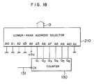
- Fig. 18 shows an example of the circuit for making access to the sub-code write region 47 of the RAM 207 of Fig. 15.
- a counter 130 of 6 bits in which the least significant bit and the most significant bit are represented by Q1 and Q2 respectively.
- the lower-rank address selection circuit 210 has input of 11 bits in which the least significant bit and the most significant bit are represented by A0 and A11.
- the counter 130 has a terminal which receives a data access command signal 131 corresponding to, for example, a sub-code input command 1 in the sub-code input address generation circuit 214.
- data has been judged to be valid when the C1 flag is "0". This means that data is considered to be valid when judgement proves that no error exists or one bite correction is executed in C1 correction.
- the standard for determining validity of data may be changed. For example, in the case where data should be considered valid only when judgement proves that correction cannot be made in C1 correction, such a circuit as shown in Fig. 19 may be used. In Fig. 19, the circuit includes an AND circuit 118.
- a C1 parity 35 is added in performing cording to the region of the RAM 207 in which the ID data 50 and the flag data 51 have been stored. Accordingly, it is necessary to read out the ID data 50 and the flag data 51 before coding is carried out. In order to read out those data prior to the coding, however, it is necessary to provide another storage circuit. If the ID data 50 and the flag data 51 are rewritten to an unused region in the RAM 207 by using RAM access for parity generation by controlling the cording address generation circuit 211 and the higher-rank address generation circuit 218, the additional provision of the storage circuit can be avoided.
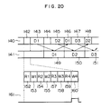
- Fig. 20 is a timing chart in the coding operation performed in the coding circuit 205.
- Data exchange between the coding circuit 205 and the RAM 207 is executed at timings on a time belt 140, while coding processing is executed at an operation time belt 141.
- Data D1 of one system and 32 words is supplied to the coding circuit 205 from the RAM 207 at a timing 143 on the time belt 140, subject to operational processing at a timing 149 on the time belt 141, and then written into the C1 parity region 35 of the RAM 207 at a timing 146 on the time belt 140. Thereafter, parity generation is performed at similar timings. Parity write timings 142, 144, 146, and 148 on the timechart 140 are shown as a write timing 160. Numerals 152, 154, 157, and 159 represent read timings from the RAM 207, while numerals 153, 155, 158, and 160 represent write timings into the RAM 207.
- the timings 158 and 159 relate to the ID data 50 and the flag data 51, and the access of the ID data 50 and the access of the flag data 51 are performed at the timings 142 and 144 respectively. If the higher-rank address of the RAM 207 is changed-over in the RAM writing operation 159 at the timings 142 and 144, the data 50 and 51 can be rewritten so that those data can be remained in another region even if parity generation is performed thereafter.
- Fig. 21 is a timechart showing an example of address timings for the data rewriting described above, in which broken lines show a period of time (15 msec) during which the rotary cylinder 220 is rotated by 180 degree.
- Fig. 21 shows the timings in the care where the RAM 207 has a capacity of 256 Kbits. In the case of the RAM of 256 Kbits, it is possible to provide eight faces of regions, one being shown in Fig. 15. Operational timings on the respective faces are shown on time belts 171 through 178.
- timing 180 at which PCM data from an A/D converter 200 is written a timing 181 at which coding is performed in the coding circuit 205, a timing 182 at which the PCM data is recorded on the magnetic tape 221, a timing 183 at which sub-code data from the demodulation circuit 300 is written, a coding timing 184 (portion hatched with horizontal lines), a timing 185 at which the sub-code data is recorded on the magnetic tape 221, a timing 186 (portion hatched with oblique lines) at which the ID data 50 and the flag data 51 are rewritten, and a timing 187 at which the ID data 50 and the flag data 51 are recorded on the magnetic tape 221.
- the ID data 50 and the flag data 51 are rewritten into the unused region, so that recording can be performed without increasing storage circuits.
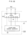
- Fig. 22 shows an example of the higher-rank address generation circuit 218 for performing the data rewriting shown in Fig. 21. It is assumed that the time belts 171 through 178 in Fig. 21 correspond to the address of the higher-rank bits of 0 through 7.
- the higher-rank address generation circuit 218 is constituted by a 3-bit adder 190 and a higher-rank address generator 191.
- a B-input of the adder 190 becomes 5 in decimal representation in the period in which a timing signal 161 shown in Fig. 20 is in a high level, so that the ID data 50 and the flag data 51 can be written at the address of the RAM 207 corresponding to the time belts 171 - 178 shown in Fig. 21.
- the C2 parity generated at the coding timing 181 and the ID data 50 and the flag data 51 which have been rewritten at the rewriting timing 186 have been written in the sub-code region 46 shown in Fig. 15. If there exists no valid data in the received ID data 50 and flag data 51 of one track (for example, when it becomes impossible to reproduce data over one track in the reproducing device due to dropout or any other reason), new sub-code data is not written in the sub-code write region 47 of the RAM 207. Accordingly, in such a condition, the C2 parity, etc. are erroneously recorded on the magnetic tape 221 as sub-code data at the sub-code record timing 185.
Landscapes
- Engineering & Computer Science (AREA)
- Multimedia (AREA)
- Signal Processing (AREA)
- Signal Processing For Digital Recording And Reproducing (AREA)
Description
- The present invention relates to a system for reproducing PCM data and sub-code data from a first recording medium and recording the PCM data and sub-code data onto a second recording medium according to
claim 1, to a PCM signal reproducing apparatus for reproducing PCM data and sub-code data according toclaim 3 and to a PCM signal recording apparatus for recording PCM data and sub-code data according toclaim 6. - European Patent Application EP-A-0 209 141 on which the preamble of
claim 1 is based discloses a PCM signal recording and reproducing apparatus, in which two memory circuits (RAMs) are provided. While PCM signals are read and written using one of the two memory circuits, PCM signals stored in the other memory circuit are error-corrected. At the end of writing with respect to the former memory circuit, the two memory circuits are interchanged to read the error-corrected PCM signals stored in the latter memory circuit. The read-out error-corrected PCM signals are then recorded on another magnetic tape, thus dispensing with a parity adding circuit necessary for recording and realizing inexpensive copying. - In a PCM signal reproducing/recording apparatus, not only main data (PCM data) but sub-code data including sub-data and sub-ID for adding auxiliary information to the PCM data are recorded on a magnetic tape. Reference is made to U.S. Patent Nos. 4,688,225, 4,544,958, and 4,549,230. The sub-code data is for recording information such as order and time of the PCM data and has information of 64 bites per set. Eight sets of the same information are recorded on one track on a tape.
- In the case where data obtained by reproducing a magnetic tape carrying sub-code data and PCM data recorded thereon is to be recorded by a recording device to obtain another magnetic tape having the same contents as that of the first-mentioned recorded magnetic tape, that is, when a so-called copying is made, it is necessary to transmit the data from a reproducing device to the recording device.
- In such a case, it is generally considered that the whole of the data reproduced by the reproducing device is transmitted to the recording device so as to be recorded as it is. However the recording device has no function to record the raw reproduced-data as it is, and therefore it is necessary that the recording device is additionally provided with a function to extract a necessary part, that is, the PCM data and sub-code data, from the received raw reproduced data to thereby reconstruct recording data. Such a function is the same as that in the reproducing device to extract the PCM data and sub-code data from the data reproduced by the reproducing device. Accordingly, provision of such a function in the recording device means that the same function is provided wastefully in each of the reproducing device and the recording device.
- It is therefore considered that the PCM data and sub-code data extracted from the data reproduced in the reproducing device are transmitted as they are to the recording device. In this case, however, there is a problem that numbers of signal lines are required because it is necessary to provide not only signal lines for transmitting the PCM data and sub-code data but signal lines for transmitting synchronizing signals.
- Further, when the sub-code data reproduced in the reproducing device is directly inputted to the recording device, data representing the validity of the sub-code data, such as flags produced as a result of error correction carried out in the reproducing device, data ID designating a format of the sub-code data, and so on, are also transmitted. In the foregoing conventional apparatus, however, data processing to judge whether the sub-code data such as flags, the data ID, or the like, is correct or not is not carried out when the sub-code data reproduced by the reproducing device is inputted directly into the recording device, and therefore there has been a possibility that data incorrectly reproduced by the reproducing device is recorded on a tape in the recording device.
- It is therefore the object of the present invention to provide a PCM signal reproducing and/or recording apparatus with improved characteristics. In order to attain the object of the present invention, a system combining a PCM signal reproducing apparatus and a PCM signal recording apparatus is provided as a system for reproducing PCM data and sub-code data from a first recording medium and recording the PCM data and sub-code data onto a second recording medium, said sub-code data having sub-data for adding auxiliary information to said PCM data, said sub-code data and said PCM data being recorded on said first and on said second recording medium in a frame format together with error detection codes for the PCM data as well as for the sub-code data, said system comprising a reproducing device for reproducing said data from the first recording medium, a recording device for recording said data on the second recording medium and transmission means for transmitting said data from the reproducing device to the recording device, in which said reproducing device includes means for reproducing said data, means for de-formatting the data reproduced and means for detecting errors in the sub-code data, and in which said recording device includes means for supplying error detection codes related to said sub-code data, means for formatting said sub-code data and said error detection codes in said frame format and means for recording said formatted data, characterized in that in each said frame sub-code data related to the same PCM data is repeated a plurality of times, said reproducing device includes means responsive to said error detection means for generating validity flags indicating the correctness or incorrectness of each of said plurality of sub-code data in said frame, and means for formatting the corrected PCM data, the sub-code data and the corresponding validity flags in a sub-frame comprising a sub-code portion, a PCM data portion and said flags and outputting the sub-frames to the transmission means, and said recording device including means for selecting a correct one out of said plurality of sub-code data in each of said sub-frames on the basis of the transmitted validity flags and means for including this correct sub-code data said plurality of times in each of said frames to be recorded.
- This system according to the invention combines the advantages of the PCM signal reproducing apparatus and the PCM signal recording apparatus. These advantages will be described in connection with the reproducing apparatus and the recording apparatus.
- Preferably, the PCM signal reproducing/recording apparatus for reproducing PCM data and sub-code data according to the present invention is arranged so that said sub-code data having sub-data for adding auxiliary information to said PCM data, said sub-code data and said PCM data being recorded on a medium together with error detection codes for the PCM data as well as for the sub-code data, said apparatus comprising a reproducing device for reproducing said data from said recording medium, in which said reproducing device includes means for reproducing said data, means for detecting errors in the sub-code data, means responsive to said error detection means for generating validity flags indicating the correctness of incorrectness of the sub-code data, means for formatting the PCM data, the sub-code data and the corresponding validity flags in a sub-frame comprising, a sub-code portion, a PCM data portion and said flags and means for outputting the said sub-frames. Only a minimum number of signal lines for transmission is required.
- The PCM signal recording apparatus for recording PCM data and sub-code data, said sub-code data having sub-data for adding auxiliary information to said PCM data, according to the present invention es arranged so that said sub-code data and said PCM data being reproduced from a medium which is recorded in a frame format together with error detection codes for the PCM data as well as for the sub-code data, in each said frame sub-code data related to the same PCM data is repeated a plurality of times, said apparatus comprising a recording device for recording said data on the said recording medium, in which said recording device includes means for receiving reproduced sub-code data and validity flags indicating the correctness or incorrectness of each of said plurality of sub-code data in said frame, means for supplying error detection codes related to said sub-code data, means for formatting said sub-code data and said error detection codes in said frame format, means for recording said formatted data, and said recording device including means for selecting a correct one out of said plurality of sub-code data on the basis of the said received validity flags, and means for including this correct sub-code data said plurality of times in each of said frames to be recorded.
- In this case, only a minimum number of signal lines for reception is required.
- Further, since the arrangement of the sub-code data is performed by the frame of the reproduced data, it is possible to make simple the operation of the recording device in which the transmitted sub-code data is received and processed to obtain a magnetic tape having the same contents as that of the reproduced magnetic tape.
- Further, since the sub-ID has program NO and control ID and the program NO and control ID are transmitted only once in one frame of the reproduced data, the task for receiving and processing the sub-data is reduced correspondingly and efficiently.
- Further, since a flag showing the state of sub-data correction is transmitted, the sub-data recording can be performed with high reliability in the recording device in which the data is received.
- In the recording apparatus, when the sub-code data is read out from a RAM so as to be recorded on a magnetic tape, only the data in the sub-code write region is made access repeatedly eight times by a record data address generation circuit so that eight sets of one and the same valid sub-code data are multiplex-recorded on the tape to thereby prevent recording of erroneous data.
- Other features and advantages of the present invention will be apparent from the following description taken in connection with the accompanying drawings, wherein:
- Fig. 1 is a block diagram showing the whole of the PCM signal reproducing/recording apparatus according to the present invention;
- Fig. 2 is a block diagram showing the reproducing device of the PCM signal reproducing/recording apparatus of Fig. 1;
- Fig. 3 shows a track format on a magnetic tape to be reproduced by the reproducing device of Fig. 2;
- Fig. 4 shows a format of a sub-data block constituting a sub-data area of each track of Fig. 3;
- Figs. 5A and 5B show an arrangement of sub-data per track;
- Fig. 6 shows an arrangement of a pack area;
- Fig. 7 shows a format of a transmission interface;
- Fig. 8 shows a format of a sub-frame;
- Fig. 9 shows patterns of a preamble of Fig. 8;
- Fig. 10 shows biphase modification;
- Fig. 11 shows a format of transmission interface for one frame of reproduced data;
- Fig. 12 shows sub-data, sub-ID and main data for two blocks transmitted with the format of Fig. 11;
- Fig. 13 shows sub-data and sub-ID for one block of reproduced data transmitted with the format of Fig. 11;
- Fig. 14 is a block diagram showing the recording device of the PCM signal reproducing/reproducing apparatus of Fig. 1;
- Fig. 15 shows an RAM map of a storage circuit of the recording device of Fig. 14;
- Figs. 16 and 19 are circuit diagrams each showing an arrangement of a higher-rank address generation circuit and a validity detection circuit in the recording device of Fig. 14;
- Fig. 17 is an operation timing chart of the address generation circuit of Fig. 16;
- Fig. 18 is an address chart for octer-writing;
- Fig. 20 is a timing chart for coding;
- Fig. 21 is a timing chart for higher-rank addresses; and
- Fig. 22 is a diagram showing an arrangement of the higher-rank address generation circuit.
- Fig. 1 shows that the PCM signal reproducing/recording apparatus according to the present invention is constituted by a reproducing
device 500 including at least amodulation circuit 20, and arecording device 1500 including at least ademodulation circuit 300. - Fig. 2 is a block diagram showing the reproducing device of the PCM signal reproducing/recording apparatus according to the present invention. In Fig. 2, the arrangement includes: a
magnetic tape 11 on which main data of PCM audio data, and sub-data, etc., are recorded; arotary drum 12 having a pair ofheads reproduction amplifier 13; ademodulation circuit 14; a memory (RAM) 16; an error correction circuit (ECU) 17; and anaddress control circuit 18. Themagnetic tape 11 has a recording format thereon as shown in Fig. 3. - In Fig. 3, the
magnetic tape 11 hassub-data area 111 and 112 in which sub-data is recorded and amain data area 113 in which main data composed of PCM audio data is recorded. In each of thesub-data areas sub-data areas 111 and 112, while 128 blocks of main data is recorded in themain data area 113. - The format of each of the 16 sub-data blocks forming each of the
sub-data areas 111 and 112 is composed of sync. sub-ID (SW1 and SW2), sub-ID parity, and sub-data (SDij, SPij : i=0 ... 15, j=0 ... 31). The sync is formed on one symbol, the sub-ID parity is formed on one symbol, and the sub-data is composed of 32 symbols. - One sub-data block has sub-data of 32 symbols, and the sub-data blocks include two kinds of blocks, one including only data, the other including not only data but parity. The respective symbols have
numbers 0 ... 31 in the order along the direction of record. The sub-data is composed of data (SD0,0 - SD15,23) and parity (SP1,24 - SP15,31) and the sub-data per track has data of 448 symbols and parity of 64 symbols. The parity is used as a code for data error detection and correction. The positioning of the sub-data is as shown in Fig. 5. - Pack ID shows the number of packs included in the sub-data in two blocks starting from an even-numbered block.
- When the data ID is "0000", the sub-data is composed of only packs, and the maximum capacity of the sub-data is 7 packs per two blocks. The number of packs used actually is indicated by the pack ID and all the remainder of the pack area of the sub-data is made to be "0".
- The pack ID of SW2 indicates the number of packs in the sub-data, and the pack areas 1 - 7 are arranged as shown in Fig. 6. The pack data is successively recorded in accordance with the area number.
- The aforementioned data recorded on the
magnetic tape 11 is reproduced by the pair ofheads rotary drum 12. After amplified by thereproduction amplifier 13, the reproduced data is demodulated by the 10-8demodulation circuit 14. The demodulated data is applied to thememory 16 through adata bus 15. - When one frame of data has been reproduced in one revolution of the
rotary drum 12, theerror correction circuit 17 corrects an error in the data by use of the parity (correction code) contained in the data and causes thememory 16 to store C₁ correction flag indicating the state of error. - The
address control circuit 18 generates a predetermined address signal in synchronism with a predetermined timing signal generated by a not-shown decoder on the basis of a data selection signal. The address signal is applied to thememory 16 through anaddress bus 19 so that the data stored in the address of thememory 16 designated by the address signal is read out through thedata bus 15. - The main data and C₁ correction flag read out from the
memory 16 are supplied to theinterface modulation circuit 20. Other than those main data and C₁ correction flag, the respective outputs from a framesync generation circuit 21, apreamble generation circuit 22, asub-ID detection circuit 23, asub-data generation circuit 24, and a main dataID detection circuit 25 are supplied to theinterface modulation circuit 20, and then, after biphase-modulated in theinterface modulation circuit 20, supplied to therecording device 1500 shown in Fig. 14. - Fig. 7 shows a format of a signal transmitted from the
modulation circuit 20 to the recording device shown in Fig. 14. In Fig. 7, the format is composed of 192 frames and each frame is composed of two sub-frames. The format of each sub-frame is composed of a preamble portion to which 4 time slots are allotted, an AUX-DATA portion to which 8 time slots are allotted, a PCM data portion to which 16 time slots are allotted, and a remainder portion of 4 times slots, as shown in Fig. 8. In other words, each sub-frame is composed of 32 time slots. The remainder portion of 4 times slots has a validity indicating bit V, a user's bit U, a channel status bit C, and a parity bit P. the validity indicating bit V, the user's bit U, and the channel status bit C are used by the 192 frames. - In the preamble portion, three kinds of patterns B, W and M are included. The pattern B is added to the CH1 at the head of a block, the pattern M is added to the CH1 other than the CH1 at the head of a block, and the pattern W is added to the head of each of the sub-frames CH2, CH3, ..... . Those patterns B, W and M have such specific patterns as shown in Fig. 9. The "1" and "0" of NRZ are modulated into biphase patterns with T and 2T as shown in Fig. 10.
- It is necessary to transmit a signal of 1440 frames during one revolution of the
rotary drum 12 when data recorded on themagnetic tape 11 is reproduced and transmitted. Fig. 11 shows the signal format at that time. As shown in Fig. 12, in the first frame in one revolution of therotary drum 12, main data L₀ is allotted to the PCM data portion, and program NO₁ of the sub-ID and control ID are allotted to the AUX-DATA portion, in the first sub-frame; and main data R₀ is allotted to the PCM data portion, and program NO₂ and program NO₃ of the sub-ID are allotted to the AUX-DATA portion, in the next sub-frame. In each sub-frame of each of the second and third frames, L₁, R₁, L₂, and R₂ are allotted to the PCM data portion and nothing is allotted to the AUX-DATA portion. In the fourth frame, L₃ is allotted to the PCM data portion and pack ID of the sub-ID and Data ID are allotted to the AUX-DATA portion in the first sub-frame, and R₃ is allotted to the PCM data portion and a C₁ flag is allotted to the AUX-DATA portion in the next sub-frame. - In the succeeding sub-frames, main data L₄, .., L₃₁, R₄, ..., R₃₁ are allotted to the respective PCM portions and packs 1, 3, 5, 7, 2, 4, 6 of sub-data are allotted in order to the AUX-DATA portions. Thus, transmission of sub-ID and sub-data for two blocks has been completed. Then, transmission of sub-data for the next two blocks is performed from the 33rd frame. In this case, the program NO and control ID of sub-ID are not transmitted but only the remainder of the sub-ID and sub-data are transmitted as shown in Fig. 13. Fig. 13 shows the sub-ID and sub-data in AUX-DATA portions transmitted in one revolution of the rotary drum, that is, in one frame of reproduced data. Since the control ID of the sub-ID does not change during one frame, only once transmission of the control ID sufficies so that the burden on the transmission side as well as the reception side can be reduced.
- To perform the above, the frame sync.
generation circuit 21 generates frame sync. in synchronism with the rotation of therotary drum 12 and thepreamble generation circuit 22 generates one of the three kinds of patterns at the head of each sub-frame on the basis of the sync., the pattern being supplied to themodulation circuit 20. Upon detection of the sub-ID in the sub-data read out from thememory 16, thesub-ID detection circuit 23 supplies various ID data of the detected sub-ID to themodulation circuit 20 at predetermined timing at the head of one revolution of the rotary drum and the head of every two blocks of the sub-data. Thesub-data generation circuit 24 generates sub-data, that is, pack data 1-7 at predetermined timing on the basis of the data read out from thememory 16 and supplies the thus generated sub-data to themodulation circuit 20. The main dataID detection circuit 25 detects various data on the basis of the data read out from thememory 16 and supplies the detected data tomodulation circuit 20 for providing V, U, C and P. - The
modulation circuit 20 biphase-modulates the main data which has been read-out from thememory 16 and supplied thereto, and supplies the biphase-modulated main data to therecording device 1500. - Fig. 14 is a block diagram of the
recording device 1500 of the PCM signal reproducing/recording apparatus. - The recording device 1500 is provided with a demodulation circuit 300 for demodulating the PCM data (main data) and sub-code data (sub-data, sub-ID, etc.) received from the modulation circuit 20 through a data input terminal 301 and for generating a sub-code input command 1; an A/D conversion circuit 200 for converting an analog signal into a PCM signal; a magnetic tape 221; a rotary cylinder 200; heads 222 and 223; a recording circuit 209 constituted by a recording amplifier and so on; a modulation circuit 208; a RAM 207 which is a storage circuit for temporarily storing data and which has a capacity of 256 Kbits; a coding circuit 205 for generating parity; a reset circuit 206 for zero-resetting the input data to the RAM 207; a write control circuit 219 for sending a write command to the RAM 207; a higher-rank address generation circuit 218 for controlling the higher-rank three bits of the address of the RAM 207; a coding address generation circuit 211 for controlling the lower-rank address of the RAM 207 so as to generate parity in the coding circuit 205; a PCM data address generation circuit 212 for controlling the lower-rank address of the RAM 207 when input is made into the RAM 207 from the A/D conversion circuit 200; a recording data address generation circuit 213 for controlling the lower-rank address of the RAM 207 when output is made from the RAM 207 into the modulation circuit 208; a sub-code input address generation circuit 214 for controlling the lower-rank address of the RAM 207 when sub-code input is made into the RAM 207; a sub clear timing generation circuit 1 for generating a timing for making clear the sub-code area of the RAM 207; a timing generation circuit 215 for controlling the operational timing of the various circuits 1, 211 - 214, and so on; a lower-rank address selection circuit 210 for selecting the lower-rank address of the RAM 207; a crystal oscillator 216; a clock detection circuit 217 for detecting existence of external clock; an audio signal input terminal; an external clock input terminal 227; and a validity detection circuit 233 for detecting whether a specific data of the sub-code is "0" or not.
- First, the operation of the
recording device 1500 of Fig. 14 will be described. - An analog signal is supplied through the audio signal input terminal and converted into a PCM signal by the A/
D conversion circuit 200. The thus converted PCM signal is stored in theRAM 207 at the address controlled by the PCM data addressgeneration circuit 212. Data is read out from theRAM 207 with the address controlled by the codingaddress generation circuit 211, and parity is generated by thecoding circuit 205 and written into theRAM 207. Then, under control by the recording dataaddress generation circuit 213, data is read out from theRAM 207, modulated in themodulation circuit 208, amplified in therecording circuit 209, and recorded on themagnetic tape 221 by theheads - On the other hand, the PCM data is supplied from the
demodulation circuit 300, stored in theRAM 207 with the address controlled by the sub-code inputaddress generation circuit 214, subject to the same processing as above, and recorded on themagnetic tape 221. - In the
RAM 207, on the other hand,sub-code data 34 andC₁ parity 35 are stored in the above operation. Fig. 15 is an RAM map showing the region where thosesub-code data 34 andC₁ parity 35 are stored. Fig. 15 shows the data storage region of one track and this one face is a capacity of one track. The sub-code is stored in the central region indicated by a thicksolid line 46. In this region, data is stored in the vertical direction along the direction of recording on the tape. This region is composed of 512 bites arranged in four columns. In Fig. 15, the coordinates represent the address of theRAM 207 with hexadecimal notation. - The
region 34 is used also as a region for the C₂ parity for the PCM data, and in the actual case of write, after PCM data has been written on themagnetic tape 221 succeeding PCM data is inputted and written in the interval before parity is generated. - A hatched
region 47 is called a sub-code write-in region which will be described later. - In the
recording device 1500, of the sub-code data transmitted by the two tracks with the format shown in Figs. 12 and 13, only one set of sub-code data consisting of check bit, data ID, and C₁ flag all of which are "0" are written in octuple onto themagnetic tape 221. - In this case, as data showing the fact that the sub-code is correct, used are check bit showing that SW1 and SW2 have been reproduced correctly, C₁ flag showing that the
sub-code data 34 has been reproduced correctly, and data ID the whole of which are written in "0". - The operation of the recording device of Fig. 14 in recording data will be described hereunder.
-
Sub-code input command 1 is supplied from thedemodulation circuit 300 and sub-code data is also inputted from thedemodulation circuit 300 in synchronism with thesub-code input command 1. The sub-code inputaddress generation circuit 214 detects the timing of input of the ID data and flag data and sends detection commands 4 and 5 to thevalidity detection circuit 233 which checks whether all the check bit, data ID and C₁ flag are "0" or not. Thevalidity detection circuit 233 sends a "0"detection signal 2 to thewrite control circuit 219 which transfers awrite command 3 to theRAM 207 so that theRAM 207 stores the sub-code data. At that time, the sub-code inputaddress generation circuit 214 makes access only to a specific region composed of 64 bites so that write is made at a specific address independently of the position of valid sub-code data. The region is called a sub-code write-in region. Upon detection of completion of transfer of the sub-code data of two tracks (64 bites) by the sub-code inputaddress generation circuit 214, thevalidity detection circuit 233 is controlled to stop the "0"detection signal 2 so as to reset thewrite command 3 to thereby terminate the storing operation into theRAM 207. Upon completion of input of the sub-code data of two tracks (1024 bites), thevalidity detection circuit 233 returns into a reset state and then performs validity detection. - Through the above operation, one set of data including check bit, data ID and C₁ all of which are "0" have been written in the sub-code write-in region of the
RAM 207. - In recording on tape, the recording data
address generation circuit 213 is caused to repeatedly make access only to the sub-code write-inregion 47 so that the sub-code data is read out from theregion 47 and recorded in the sub-code recording area on the tape. Thus, valid data can be recorded in octuple on the tape. - As described above, in the
recording device 1500, it is possible to prevent recording of sub-code data having errors and sub-code data having a format other than a specified one. - Fig. 16 shows an example of the sub-code input
address generation circuit 214 and thevalidity detection circuit 233. In Fig. 16, the sub-code inputaddress generation circuit 214 includes acounter 70 and atiming decoding circuit 71 for deriving a necessary timing from thecounter 70, and thevalidity detection circuit 233 includes latches 72 - 75, OR circuits 76 - 78, an ANDcircuit 79, NAND circuits 80 - 83, and inverters 84 - 88. Thereference numeral 5 represents a clear signal. Each of thecounter 70, and the latch circuits 72 - 75 is actuated to operate at a trailing edge of a clock. The reset of thelatch circuits latch circuit 75 is actuated by a low level. The Q-output signal 113 of thelatch circuit 75 is inverted by theinverter 88 so that thesub-code input command 1 is gated by the ANDcircuit 79 and transferred as the "0"detection signal 2 into thewrite control circuit 219. Accordingly, control is made so that the input sub-code data is written into theRAM 207 when thesignal 113 is in low level while the write is inhibited when thesignal 113 is in high level. - The
reference numerals - Further, "LSB" and "MSB" labeled at the input
sub-code data 6 represent the least significant bit and the most significant bit respectively. - Referring to a timing chart of Fig. 17, the operation of the circuit in Fig. 16 will be described hereunder. Fig. 17 shows the operation in the case where only the third set of ID data and flag data are indicated to be valid (hatched data).
- Upon input of the
clear signal 107, thelatch circuits signal 101 is high, thesignals sub-code data 6 is written in theRAM 207. - At a
timing 66 in alatch clock 4, if any of a check bit 61, a data ID 41, and a C₁ flag is "1", the high level is latched by thelatch circuit output 104 of theOR circuit 78 is made high, and theoutput 115 of theinverter 87 is made low, so that theoutput 108 of theNAND circuit 84 becomes high. Accordingly, the high level is latched by thelatch circuit 75 at a trailingedge 91 of asignal 109, and thesignal 113 becomes high to thereby inhibit write of the RAM (hereinafter referred to as "RAM write"). Theoutput 105 of theNAND circuit 82 is low, so that thesignal 106 is left as it is in low level at a trailingedge 92 of asignal 110. - Succeedingly, the
latch circuit 75 is reset by the low section of thesignal 101, thesignal 113 becomes low, and the RAM write is started. - As described above, the RAM write of a
sub-code data 121 located between theedge 91 and thesection 93 can be inhibited. By operating thetiming - If all the check bit, the data ID, and the C₁ flag are "0" at a timing 68, both the
latch circuits signal 104 is changed to low. Accordingly, thesignals signal 108 becomes low, and the low level is latched at a trailingedge 97 of thesignal 109, so that thesignal 113 is left in low as it is. Accordingly, the state of RAM write is maintained. Theoutput 106 of thelatch circuit 74 and the signal 114 become high and low respectively at a trailingedge 98 of thesignal 110, so that the level of thesignal 105 is not influenced by thesignal 104 until theclear signal 107 is inputted to reset thelatch circuit 74. - Thereafter, in a high section 120 of a
signal 100, thesignal 106 is high, thelatch circuit 75 is set, and thesignal 113 becomes high, so that the RAM write is inhibited. Then, thesignal 106 is high, so that thelatch circuit 75 is not reset by thesignal 101, and thesignal 113 is kept high independently of the level of thesignal 104. - As described above,
ID data 50, flag data 51 (portions hatched with oblique lines), andsub-code data 123 can be written in theRAM 207, and then thesub-code data 123 is never rewritten until theclear signal 107 is produced. Although six data between thetiming 99 through 120 are arranged to be written in theRAM 207, all the first six-data are "1", so that there is problem. - Fig. 18 shows an example of the circuit for making access to the
sub-code write region 47 of theRAM 207 of Fig. 15. In Fig. 18, there is provided acounter 130 of 6 bits in which the least significant bit and the most significant bit are represented by Q₁ and Q₂ respectively. The lower-rankaddress selection circuit 210 has input of 11 bits in which the least significant bit and the most significant bit are represented by A₀ and A₁₁. Thecounter 130 has a terminal which receives a dataaccess command signal 131 corresponding to, for example, asub-code input command 1 in the sub-code inputaddress generation circuit 214. - By fixedly maintaining the input bits A₀ through A₃ and A₁₁ at a low level and the input bit A₄ at a high level, access can be made to the address only in the
sub-code write region 47 of theRAM 207. - In the embodiment described above, data has been judged to be valid when the C₁ flag is "0". This means that data is considered to be valid when judgement proves that no error exists or one bite correction is executed in C₁ correction. However, the standard for determining validity of data may be changed. For example, in the case where data should be considered valid only when judgement proves that correction cannot be made in C₁ correction, such a circuit as shown in Fig. 19 may be used. In Fig. 19, the circuit includes an AND
circuit 118. - A
C₁ parity 35 is added in performing cording to the region of theRAM 207 in which theID data 50 and theflag data 51 have been stored. Accordingly, it is necessary to read out theID data 50 and theflag data 51 before coding is carried out. In order to read out those data prior to the coding, however, it is necessary to provide another storage circuit. If theID data 50 and theflag data 51 are rewritten to an unused region in theRAM 207 by using RAM access for parity generation by controlling the cordingaddress generation circuit 211 and the higher-rankaddress generation circuit 218, the additional provision of the storage circuit can be avoided. - Fig. 20 is a timing chart in the coding operation performed in the
coding circuit 205. Data exchange between thecoding circuit 205 and theRAM 207 is executed at timings on atime belt 140, while coding processing is executed at anoperation time belt 141. - Data D₁ of one system and 32 words is supplied to the
coding circuit 205 from theRAM 207 at atiming 143 on thetime belt 140, subject to operational processing at atiming 149 on thetime belt 141, and then written into theC₁ parity region 35 of theRAM 207 at atiming 146 on thetime belt 140. Thereafter, parity generation is performed at similar timings. Parity writetimings timechart 140 are shown as awrite timing 160.Numerals RAM 207, whilenumerals 153, 155, 158, and 160 represent write timings into theRAM 207. Of those timings, thetimings 158 and 159 relate to theID data 50 and theflag data 51, and the access of theID data 50 and the access of theflag data 51 are performed at thetimings RAM 207 is changed-over in theRAM writing operation 159 at thetimings data - Fig. 21 is a timechart showing an example of address timings for the data rewriting described above, in which broken lines show a period of time (15 msec) during which the
rotary cylinder 220 is rotated by 180 degree. Fig. 21 shows the timings in the care where theRAM 207 has a capacity of 256 Kbits. In the case of the RAM of 256 Kbits, it is possible to provide eight faces of regions, one being shown in Fig. 15. Operational timings on the respective faces are shown ontime belts 171 through 178. There are provided atiming 180 at which PCM data from an A/D converter 200 is written, atiming 181 at which coding is performed in thecoding circuit 205, atiming 182 at which the PCM data is recorded on themagnetic tape 221, atiming 183 at which sub-code data from thedemodulation circuit 300 is written, a coding timing 184 (portion hatched with horizontal lines), atiming 185 at which the sub-code data is recorded on themagnetic tape 221, a timing 186 (portion hatched with oblique lines) at which theID data 50 and theflag data 51 are rewritten, and atiming 187 at which theID data 50 and theflag data 51 are recorded on themagnetic tape 221. - As shown in Fig. 21, the
ID data 50 and theflag data 51 are rewritten into the unused region, so that recording can be performed without increasing storage circuits. - Fig. 22 shows an example of the higher-rank
address generation circuit 218 for performing the data rewriting shown in Fig. 21. It is assumed that thetime belts 171 through 178 in Fig. 21 correspond to the address of the higher-rank bits of 0 through 7. In Fig. 22, the higher-rankaddress generation circuit 218 is constituted by a 3-bit adder 190 and a higher-rank address generator 191. A B-input of theadder 190 becomes 5 in decimal representation in the period in which atiming signal 161 shown in Fig. 20 is in a high level, so that theID data 50 and theflag data 51 can be written at the address of theRAM 207 corresponding to the time belts 171 - 178 shown in Fig. 21. - Just before the sub-code data is stored in the
RAM 207 at the sub-code input timing 183 shown in Fig. 21, the C₂ parity generated at thecoding timing 181 and theID data 50 and theflag data 51 which have been rewritten at therewriting timing 186 have been written in thesub-code region 46 shown in Fig. 15. If there exists no valid data in the receivedID data 50 andflag data 51 of one track (for example, when it becomes impossible to reproduce data over one track in the reproducing device due to dropout or any other reason), new sub-code data is not written in thesub-code write region 47 of theRAM 207. Accordingly, in such a condition, the C₂ parity, etc. are erroneously recorded on themagnetic tape 221 as sub-code data at thesub-code record timing 185. - If "0" data is written, by using the
reset circuit 206, in both thesub-code region 46 and thesub-code write region 47 at sub-codeclear timings 302 shown in Fig. 21, the above-mentioned C₂ parity, etc. can be cleared, so that the "0" data is recorded on themagnetic tape 221 as the sub-code data even when there exists no valid data in the input sub-code data over one track to thereby make it possible to solve the problem described above.
Claims (9)
- A system for reproducing PCM data and sub-code data from a first recording medium and recording the PCM data and sub-code data onto a second recording medium, said sub-code data having sub-data for adding auxiliary information to said PCM data, said sub-code data and said PCM data being recorded on said first and on said second recording medium in a frame format together with error detection codes for the PCM data as well as for the sub-code data, said system comprising a reproducing device (500) for reproducing said data from the first recording medium, a recording device for recording said data on the second recording medium and transmission means for transmitting said data from the reproducing device to the recording device,
in which said reproducing device (500) includes means for reproducing said data, means for de-formatting the data reproduced and means for detecting errors in the sub-code data, and in which said recording device (1500) includes means for supplying error detection codes related to said sub-code data, means for formatting said sub-code data and said error detection codes in said frame format and means for recording said formatted data, characterized in that in each said frame sub-code data related to the same PCM data is repeated a plurality of times, said reproducing device (500) includes means responsive to said error detection means for generating validity flags indicating the correctness or incorrectness of each of said plurality of sub-code data in said frame, and means for formatting the corrected PCM data, the sub-code data and the corresponding validity flags in a sub-frame comprising a sub-code portion, a PCM data portion and said flags and outputting the sub-frames to the transmission means, and said recording device (1500) including means for selecting a correct one out of said plurality of sub-code data in each of said sub-frames on the basis of the transmitted validity flags and means for including this correct sub-code data said plurality of times in each of said frames to be recorded. - A system according to claim 1, said sub-code data including program number and ID code, so that said reproducing device (500) outputs said program number and ID code only once for every said frame.
- A PCM signal reproducing apparatus for reproducing PCM data and sub-code data, said sub-code data having sub-data for adding auxiliary information to said PCM data, said sub-code data and said PCM data being recorded on a medium together with error detection codes for the PCM data as well as for the sub-code data, said apparatus comprising a reproducing device (500) for reproducing said data from said recording medium, in which said reproducing device (500) includes means for reproducing said data, means for detecting errors in the sub-code data, means responsive to said error detection means for generating validity flags indicating the correctness of incorrectness of the sub-code data, means for formatting the PCM data, the sub-code data and the corresponding validity flags in a sub-frame comprising, a sub-code portion, a PCM data portion and said flags and means for outputting the said sub-frames.
- A PCM signal reproducing apparatus according to claim 3, said sub-code data and said PCM data being recorded on the said medium in a frame format, and in which the formatting of the said sub-frame is performed by the said frame.
- A PCM signal reproducing apparatus according to claim 4, said sub-code data including program number and ID code, so that said reproducing device (500) outputs said program number and ID code only once for every said frame.
- A PCM signal recording apparatus for recording PCM data and sub-code data, said sub-code data having sub-data for adding auxiliary information to said PCM data, said sub-code data and said PCM data being reproduced from a medium which is recorded in a frame format together with error detection codes for the PCM data as well as for the sub-code data, in each said frame sub-code data related to the same PCM data is repeated a plurality of times, said apparatus comprising a recording device (1500) for recording said data on the said recording medium, in which said recording device (1500) includes means for receiving reproduced sub-code data and validity flags indicating the correctness or incorrectness of each of said plurality of sub-code data in said frame, means for supplying error detection codes related to said sub-code data, means for formatting said sub-code data and said error detection codes in said frame format, means for recording said formatted data, and said recording device (1500) including means for selecting a correct one out of said plurality of sub-code data on the basis of the said received validity flags, and means for including this correct sub-code data said plurality of times in each of said frames to be recorded.
- A PCM signal recording apparatus according to claim 6, in which said recording device (1500) includes a storage circuit (207) for storing said received sub-code data, a validity flag detection circuit (233) for judging specific data indicating whether said sub-code data is correct of incorrect, a write control circuit (219) for sending a write command to said storage circuit in accordance with a result of judgement by said validity flag detection circuit, a sub-code input address generation circuit (214) for controlling addresses of said storage circuit (207) so as to store said sub-code data in a specific region of said storage circuit (207), and means for storing only the correct sub-code data detected by said validity flag detection circuit.
- A PCM signal recording apparatus according to claim 7, said recording device includes a record data address generation circuit (213) for controlling the addresses of said storage circuit so as to read out said sub-code data stored in said specific region of said storage circuit, N-times repeatedly from said storage circuit, and means for recording said sub-code data stored in said specific region of said storage circuit onto the recording medium N-times.
- A PCM signal recording apparatus according to claim 6, said recording device further including means for recording fixed sub-code data, when the correct sub-code data is not detected by the said selecting means in each of said frames.
Applications Claiming Priority (4)
| Application Number | Priority Date | Filing Date | Title |
|---|---|---|---|
| JP199866/87 | 1987-08-12 | ||
| JP19986687A JPH0661153B2 (en) | 1987-08-12 | 1987-08-12 | PCM signal recorder |
| JP205020/87 | 1987-08-20 | ||
| JP20502087 | 1987-08-20 |
Publications (3)
| Publication Number | Publication Date |
|---|---|
| EP0303230A2 EP0303230A2 (en) | 1989-02-15 |
| EP0303230A3 EP0303230A3 (en) | 1991-04-24 |
| EP0303230B1 true EP0303230B1 (en) | 1994-06-01 |
Family
ID=26511804
Family Applications (1)
| Application Number | Title | Priority Date | Filing Date |
|---|---|---|---|
| EP88112939A Expired - Lifetime EP0303230B1 (en) | 1987-08-12 | 1988-08-09 | PCM signal reproducing/recording apparatus |
Country Status (3)
| Country | Link |
|---|---|
| US (1) | US5084788A (en) |
| EP (1) | EP0303230B1 (en) |
| DE (1) | DE3889804T2 (en) |
Families Citing this family (3)
| Publication number | Priority date | Publication date | Assignee | Title |
|---|---|---|---|---|
| US5200864A (en) * | 1989-06-28 | 1993-04-06 | International Business Machines Corporation | Combining small records into a single record block for recording on a record media |
| US5589994A (en) * | 1992-08-21 | 1996-12-31 | Mitsubishi Denki Kabushiki Kaisha | Image recording method and apparatus with reduced error propagation |
| US20040264391A1 (en) * | 2003-06-26 | 2004-12-30 | Motorola, Inc. | Method of full-duplex recording for a communications handset |
Family Cites Families (7)
| Publication number | Priority date | Publication date | Assignee | Title |
|---|---|---|---|---|
| JPS59119519A (en) * | 1982-12-27 | 1984-07-10 | Sony Corp | Recorder of pcm signal |
| JPS59124010A (en) * | 1982-12-29 | 1984-07-18 | Sony Corp | Recording method of pcm signal |
| JPH0661156B2 (en) * | 1983-05-21 | 1994-08-10 | ソニー株式会社 | Encoding method for error correction |
| US4622600A (en) * | 1983-12-26 | 1986-11-11 | Hitachi, Ltd. | Rotary-head type PCM data recording/reproducing method and apparatus with a redundancy-reduced control data format |
| JPS6220180A (en) * | 1985-07-19 | 1987-01-28 | Hitachi Ltd | Pcm signal recording and reproducing device |
| CA1303729C (en) * | 1985-09-03 | 1992-06-16 | Tetsuro Kato | Method and apparatus for recording and/or reproducing a pcm signal |
| JP2751150B2 (en) * | 1986-03-11 | 1998-05-18 | ソニー株式会社 | Magnetic tape recording device and reproducing device |
-
1988
- 1988-08-09 EP EP88112939A patent/EP0303230B1/en not_active Expired - Lifetime
- 1988-08-09 DE DE3889804T patent/DE3889804T2/en not_active Expired - Fee Related
- 1988-08-11 US US07/231,001 patent/US5084788A/en not_active Expired - Fee Related
Also Published As
| Publication number | Publication date |
|---|---|
| EP0303230A2 (en) | 1989-02-15 |
| DE3889804D1 (en) | 1994-07-07 |
| US5084788A (en) | 1992-01-28 |
| EP0303230A3 (en) | 1991-04-24 |
| DE3889804T2 (en) | 1994-09-08 |
Similar Documents
| Publication | Publication Date | Title |
|---|---|---|
| CA1292565C (en) | Data recorder and method | |
| CA1322405C (en) | Method and apparatus for recording and/or reproducing digital data | |
| EP0209141B1 (en) | Pcm signal recording and reproducing apparatus | |
| US7019927B2 (en) | Information signal recording and playback method and apparatus therefor | |
| EP0224929A2 (en) | Apparatus and method for preventing unauthorized dubbing of a recording signal | |
| EP0429727B1 (en) | Data recorder | |
| JPH0444342B2 (en) | ||
| US5182678A (en) | PCM signal reproducing/recording apparatus | |
| EP0303230B1 (en) | PCM signal reproducing/recording apparatus | |
| EP0294841A2 (en) | Memory control system | |
| EP0272917B1 (en) | Apparatus for storing digital data | |
| US4872171A (en) | Method for recording digital data so as to avoid operational error on reproduction | |
| EP0694922A2 (en) | Data recording method | |
| JPH0580749B2 (en) | ||
| JP2576535B2 (en) | Data recorder | |
| KR900007373B1 (en) | Digital signal demodulator | |
| JP2637727B2 (en) | Playback signal processing method | |
| US4864571A (en) | Information recording/reproducing apparatus with prioritized read out | |
| JPH0666106B2 (en) | Error detection circuit | |
| JP2661067B2 (en) | Data recorder | |
| JP2724632B2 (en) | Multi-track digital tape recorder | |
| JPH01258271A (en) | Pcm signal magnetic regenerating device | |
| JPH0542069B2 (en) | ||
| JP2576551B2 (en) | Data recorder | |
| JP2634407B2 (en) | Error correction device for digital audio signal |
Legal Events
| Date | Code | Title | Description |
|---|---|---|---|
| PUAI | Public reference made under article 153(3) epc to a published international application that has entered the european phase |
Free format text: ORIGINAL CODE: 0009012 |
|
| 17P | Request for examination filed |
Effective date: 19880809 |
|
| AK | Designated contracting states |
Kind code of ref document: A2 Designated state(s): DE FR GB |
|
| PUAL | Search report despatched |
Free format text: ORIGINAL CODE: 0009013 |
|
| AK | Designated contracting states |
Kind code of ref document: A3 Designated state(s): DE FR GB |
|
| 17Q | First examination report despatched |
Effective date: 19921008 |
|
| GRAA | (expected) grant |
Free format text: ORIGINAL CODE: 0009210 |
|
| AK | Designated contracting states |
Kind code of ref document: B1 Designated state(s): DE FR GB |
|
| REF | Corresponds to: |
Ref document number: 3889804 Country of ref document: DE Date of ref document: 19940707 |
|
| ET | Fr: translation filed | ||
| PLBE | No opposition filed within time limit |
Free format text: ORIGINAL CODE: 0009261 |
|
| STAA | Information on the status of an ep patent application or granted ep patent |
Free format text: STATUS: NO OPPOSITION FILED WITHIN TIME LIMIT |
|
| 26N | No opposition filed | ||
| PGFP | Annual fee paid to national office [announced via postgrant information from national office to epo] |
Ref country code: FR Payment date: 19980616 Year of fee payment: 11 |
|
| PGFP | Annual fee paid to national office [announced via postgrant information from national office to epo] |
Ref country code: GB Payment date: 19980730 Year of fee payment: 11 |
|
| PGFP | Annual fee paid to national office [announced via postgrant information from national office to epo] |
Ref country code: DE Payment date: 19980928 Year of fee payment: 11 |
|
| PG25 | Lapsed in a contracting state [announced via postgrant information from national office to epo] |
Ref country code: GB Free format text: LAPSE BECAUSE OF NON-PAYMENT OF DUE FEES Effective date: 19990809 |
|
| GBPC | Gb: european patent ceased through non-payment of renewal fee |
Effective date: 19990809 |
|
| PG25 | Lapsed in a contracting state [announced via postgrant information from national office to epo] |
Ref country code: FR Free format text: LAPSE BECAUSE OF NON-PAYMENT OF DUE FEES Effective date: 20000428 |
|
| PG25 | Lapsed in a contracting state [announced via postgrant information from national office to epo] |
Ref country code: DE Free format text: LAPSE BECAUSE OF NON-PAYMENT OF DUE FEES Effective date: 20000601 |
|
| REG | Reference to a national code |
Ref country code: FR Ref legal event code: ST |