EP0302584A2 - Improvements in or relating to microwave phase shifters - Google Patents
Improvements in or relating to microwave phase shifters Download PDFInfo
- Publication number
- EP0302584A2 EP0302584A2 EP88305072A EP88305072A EP0302584A2 EP 0302584 A2 EP0302584 A2 EP 0302584A2 EP 88305072 A EP88305072 A EP 88305072A EP 88305072 A EP88305072 A EP 88305072A EP 0302584 A2 EP0302584 A2 EP 0302584A2
- Authority
- EP
- European Patent Office
- Prior art keywords
- transistor
- transistors
- transmission line
- drain
- line
- Prior art date
- Legal status (The legal status is an assumption and is not a legal conclusion. Google has not performed a legal analysis and makes no representation as to the accuracy of the status listed.)
- Ceased
Links
Images


Classifications
-
- H—ELECTRICITY
- H01—ELECTRIC ELEMENTS
- H01P—WAVEGUIDES; RESONATORS, LINES, OR OTHER DEVICES OF THE WAVEGUIDE TYPE
- H01P1/00—Auxiliary devices
- H01P1/18—Phase-shifters
- H01P1/185—Phase-shifters using a diode or a gas filled discharge tube
Definitions
- This invention relates to microwave phase shifting devices and to transmission lines including such devices.
- a transmission line for transmitting microwave signals in which it is desired to produce a predetermined substantially constant phase shift, comprising a Gallium Arsenide Field Effect Transistor serially included in the line, a first section of the line terminating at the source electrode of the transistor and a second section of the line originating at the drain electrode of the transistor and control means for applying a potential to the gate electrode to switch the transistor on or off, as required, to introduce the shift of phase in a transmitted microwave signal.
- a phase shifting device for serial inclusion in a microwave transmission line, the device comprising a pair of disimilar Gallium Arsenide Field Effect Transistors, each having its source connected to the source of the other transistor to form a first terminal of the device and its drain connected to the drain of the other transistor to form a second terminal of the device, and the gates of the transistor being brought out separately so that each transistor may be switched on independantly of the other.
- Figure 1 shows a microwave transmission line 10 interrupted for the known serial inclusion therein of a phase shifting device 11.
- the device 11, shown diagrammatically in Figure 1, has terminals 12, 13 for connection respectively to sections 10 a and 10 b of the line 10.
- the device 11 is a GaAs (Gallium Arsenide) FET (Field Effective Transistor).
- the terminal 12 is electrically connected to the source electrode 14 of the device 11, and the terminal 13 is electrically connected to the drain electrode 15 of device 11.
- a gate electrode 16 of the device 11 is brought out to a terminal 17 whereto a source of potential (not shown) may be connected to turn the device on.
- the device 11 is elongate so as to ensure a relatively large inter-electrode capacitance when the device 11 is turned off and a low channel resistance when the device 11 is turned on.
- the capacitance and resistance can be measured for the device in its two states. Additionally, there will be stray capacitancies and stray inductances but these will remain substantially constant when the device has been included in a transmission line.
- Such a device can be used in transmission lines wherealong microwave signals (of frequency > 1GHz) are transmitted with a phase shift of the order of less than 10°.
- the use of a single device 11 is disadvantageous as, although a phase shift is achieved, it is only achieved at the expense of what may be an unacceptable power loss.
- the device 111 has terminals 112 and 113 for connection serially in a microwave transmission line 110
- the device 111 comprises two parallelly connected GaAs FETs.
- the terminal 112 is electrically connected to the source electrode 114 a of a first of the transistors and to the source electrode 114 b of the second transistor.
- the terminal 113 is electrically connected to the drain electrode 115 a of the first transistor and to the drain electrode 115 b of the second transistor.
- the respective gate electrodes 116 a and 116 b are brought out to respective external points 117 a and 117 b to enable a source of potential to be connected to either of the gates to switch on the respective transistor.
- FIGS. 3 and 4 of the drawings illustrate in more detail and to an enlarged scale, the form taken by each of the transistors.
- the source and drain contacts 14 and 15 are laid upon respective active mesa regions 18, 19 of a GaAs substrate 21.
- a gate electrode 16 is interposed between the electrodes 14 and 15 on a mesa region 20.
- the two transistors of the device may be simultaneously formed on the same substrate.
- the source and drain regions 18, 19 and the gate region 20 are elongate, that is, the length of each of these regions is a multiple of the width (seen in Figure 4). In this way, by variation during manufacture of this multiple, the effective inter-electrode capacitance (when switched off) and the inter-electrode resistance (when switched on) can be predetermined with reasonable accuracy.
- Figures 5 a and 5 d show the "both transistors on” and the “both transistors off” states where a phase shift is achieved in a microwave transmission between the two states. As the transistors are in parallel, they act as a single device and hence also have the disadvantage of power loss associated therewith as in the case of the prior art device of Figure 1.
- the invention is not confined to the precise details of the foregoing examples and variations may be made thereto.
- the two transistors may be separately formed.
- the device in its preferred form, is capable of introducing a phase shift of the order of 5° in a microwave transmission having a bandwidth extending from 4 to 7 GHz. Where the microwave signals are of even higher frequency, an appropriate device, in accordance with the present invention, could effect phase shifts in excess of 20°.
Landscapes
- Networks Using Active Elements (AREA)
- Waveguide Switches, Polarizers, And Phase Shifters (AREA)
Abstract
Description
- This invention relates to microwave phase shifting devices and to transmission lines including such devices.
- Difficulties are experienced in introducing controlled small e.g. less than 10° constant phase shifts in transmitted microwave signals (of frequency greater than 1GHz). Present microwave switched filter networks suffer from parasitic inductances and capacitances in the components thereof making the attainment of a controlled small, constant phase shift difficult and/or of narrow bandwidth and/or very expensive.
- It is an object of the present invention to provide a device which utilises the parasitic factors in achieving a controlled, substantially constant, broad bandwidth phase shift for microwave signals.
- It is known to provide a transmission line, for transmitting microwave signals in which it is desired to produce a predetermined substantially constant phase shift, comprising a Gallium Arsenide Field Effect Transistor serially included in the line, a first section of the line terminating at the source electrode of the transistor and a second section of the line originating at the drain electrode of the transistor and control means for applying a potential to the gate electrode to switch the transistor on or off, as required, to introduce the shift of phase in a transmitted microwave signal.
- According to the present invention, there is provided a phase shifting device, for serial inclusion in a microwave transmission line, the device comprising a pair of disimilar Gallium Arsenide Field Effect Transistors, each having its source connected to the source of the other transistor to form a first terminal of the device and its drain connected to the drain of the other transistor to form a second terminal of the device, and the gates of the transistor being brought out separately so that each transistor may be switched on independantly of the other.
- The invention will be described further, by way of example, with reference to the accompanying drawings, in which:-
- Figure 1 is a diagrammatic representation of a transmission line including a phase shifting device, as known in the prior art;
- Figure 2 is a diagrammatic representation of a phase shifting device in accordance with the present invention;
- Figure 3 and 4 are respectively plan and cross-sectional representations of a Gallium Arsenide Field Effect Transistor for insertion in a microwave transmission line whereby to effect a phase shift, in accordance with the present invention; and
- Figures 5a to d are diagrammatic representations of the equivalent circuit of the phase shifting device of the present invention.
- Referring to the drawings, Figure 1 shows a
microwave transmission line 10 interrupted for the known serial inclusion therein of aphase shifting device 11. Thedevice 11, shown diagrammatically in Figure 1, hasterminals sections line 10. Thedevice 11 is a GaAs (Gallium Arsenide) FET (Field Effective Transistor). Theterminal 12 is electrically connected to thesource electrode 14 of thedevice 11, and theterminal 13 is electrically connected to thedrain electrode 15 ofdevice 11. Agate electrode 16 of thedevice 11 is brought out to aterminal 17 whereto a source of potential (not shown) may be connected to turn the device on. - It will be noted that the
device 11 is elongate so as to ensure a relatively large inter-electrode capacitance when thedevice 11 is turned off and a low channel resistance when thedevice 11 is turned on. - The capacitance and resistance can be measured for the device in its two states. Additionally, there will be stray capacitancies and stray inductances but these will remain substantially constant when the device has been included in a transmission line.
- If a microwave transmission is effected along the
line 10 with the device turned on, and thereafter the device is turned off by removing the potential applied to thegate 16, a predeterminable phase shift will occur in the transmitted microwave signals. Similarly, when the device is turned on after having been turned off, the phase relationship of the microwave signals is restored to its former value. - Such a device can be used in transmission lines wherealong microwave signals (of frequency > 1GHz) are transmitted with a phase shift of the order of less than 10°. However, the use of a
single device 11 is disadvantageous as, although a phase shift is achieved, it is only achieved at the expense of what may be an unacceptable power loss. - This power loss disadvantage can be overcome, in accordance with the present invention, by the use of a phase shifting device as shown in Figure 2. The
device 111 hasterminals microwave transmission line 110 - The
device 111 comprises two parallelly connected GaAs FETs. Theterminal 112 is electrically connected to thesource electrode 114a of a first of the transistors and to thesource electrode 114b of the second transistor. Similarly, theterminal 113 is electrically connected to thedrain electrode 115a of the first transistor and to thedrain electrode 115b of the second transistor. - The
respective gate electrodes external points - Figures 3 and 4 of the drawings illustrate in more detail and to an enlarged scale, the form taken by each of the transistors. The source and
drain contacts active mesa regions GaAs substrate 21. Agate electrode 16 is interposed between theelectrodes mesa region 20. The two transistors of the device may be simultaneously formed on the same substrate. - As can be seen particularly on Figure 3, the source and
drain regions gate region 20 are elongate, that is, the length of each of these regions is a multiple of the width (seen in Figure 4). In this way, by variation during manufacture of this multiple, the effective inter-electrode capacitance (when switched off) and the inter-electrode resistance (when switched on) can be predetermined with reasonable accuracy. - Referring back to Figure 2, it will be seen that the lengths of the two transistors differ by approximately a factor of two and their characteristics capacitances and resistances will therefore differ.
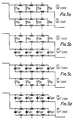
- Referring to Figures 5a to 5d, the equivalent circuits of the device of Figure 2 are diagrammatically illustrated for the four states available.
- Figures 5a and 5d show the "both transistors on" and the "both transistors off" states where a phase shift is achieved in a microwave transmission between the two states. As the transistors are in parallel, they act as a single device and hence also have the disadvantage of power loss associated therewith as in the case of the prior art device of Figure 1.
- The preferred mode of operation is illustrated in Figures 5b and 5c where one of the transistors is switched on whilst the other is switched off and the state is reversed to one where the first transistor is switched off and the second transistor is switched on. When this second transistor is switched on, a substantially constant, broadband phase shift is achieved in a microwave signal transmitted along a transmission line including the device and with a very low power loss (for example, of the order of 0.5db). The original phase relationship can be restored by switching the transistors back to their original states.
- The invention is not confined to the precise details of the foregoing examples and variations may be made thereto. For instance, in the device of Figure 2, the two transistors may be separately formed.
- Appropriate control means are provided (though not shown) for switching between the states illustrated by the equivalent circuits diagrammatically shown in Figures 5b and 5c.
- The device, in its preferred form, is capable of introducing a phase shift of the order of 5° in a microwave transmission having a bandwidth extending from 4 to 7 GHz. Where the microwave signals are of even higher frequency, an appropriate device, in accordance with the present invention, could effect phase shifts in excess of 20°.
Claims (7)
Applications Claiming Priority (2)
| Application Number | Priority Date | Filing Date | Title |
|---|---|---|---|
| GB8718651 | 1987-08-06 | ||
| GB8718651A GB2207805B (en) | 1987-08-06 | 1987-08-06 | Improvements in or relating to microwave phase shifters |
Publications (2)
| Publication Number | Publication Date |
|---|---|
| EP0302584A2 true EP0302584A2 (en) | 1989-02-08 |
| EP0302584A3 EP0302584A3 (en) | 1990-08-29 |
Family
ID=10621922
Family Applications (1)
| Application Number | Title | Priority Date | Filing Date |
|---|---|---|---|
| EP88305072A Ceased EP0302584A3 (en) | 1987-08-06 | 1988-06-03 | Improvements in or relating to microwave phase shifters |
Country Status (4)
| Country | Link |
|---|---|
| US (1) | US4853658A (en) |
| EP (1) | EP0302584A3 (en) |
| JP (1) | JPS6455901A (en) |
| GB (1) | GB2207805B (en) |
Families Citing this family (3)
| Publication number | Priority date | Publication date | Assignee | Title |
|---|---|---|---|---|
| GB2211987B (en) * | 1987-10-30 | 1992-01-02 | Plessey Co Plc | Circuit arrangement including an inductor and a mesfet |
| JP2898470B2 (en) * | 1992-05-08 | 1999-06-02 | 三菱電機株式会社 | Switched line type phase shifter |
| KR102409913B1 (en) | 2017-12-06 | 2022-06-16 | 삼성전자주식회사 | Solder reflow apparatus and method of manufacturing an electronic device |
Family Cites Families (10)
| Publication number | Priority date | Publication date | Assignee | Title |
|---|---|---|---|---|
| US3855613A (en) * | 1973-06-22 | 1974-12-17 | Rca Corp | A solid state switch using an improved junction field effect transistor |
| GB1568055A (en) * | 1975-10-17 | 1980-05-21 | Secr Defence | Field-effect transistors |
| US4161705A (en) * | 1977-12-19 | 1979-07-17 | International Telephone And Telegraph Corporation | Low level controllable radio frequency phase shifter |
| US4387386A (en) * | 1980-06-09 | 1983-06-07 | The United States Of America As Represented By The Secretary Of The Army | Microwave controlled field effect switching device |
| US4605912A (en) * | 1981-12-03 | 1986-08-12 | General Electric Company | Continuously variable phase shifting element comprised of interdigitated electrode MESFET |
| US4471330A (en) * | 1982-11-01 | 1984-09-11 | General Electric Company | Digital phase bit for microwave operation |
| JPS6041812A (en) * | 1983-08-17 | 1985-03-05 | Fujitsu Ltd | Phase shifter |
| US4647789A (en) * | 1984-09-14 | 1987-03-03 | Rca Corporation | Active element microwave phase shifter |
| EP0226154A3 (en) * | 1985-12-20 | 1989-02-15 | Allied Corporation | Monolithic dual-gate gaas fet digital phase shifter with gain |
| GB8713403D0 (en) * | 1987-06-09 | 1987-07-15 | Plessey Co Plc | Semiconductor device |
-
1987
- 1987-08-06 GB GB8718651A patent/GB2207805B/en not_active Expired - Lifetime
-
1988
- 1988-06-03 EP EP88305072A patent/EP0302584A3/en not_active Ceased
- 1988-06-27 US US07/211,705 patent/US4853658A/en not_active Expired - Fee Related
- 1988-08-04 JP JP63193581A patent/JPS6455901A/en active Pending
Also Published As
| Publication number | Publication date |
|---|---|
| GB2207805B (en) | 1991-12-11 |
| JPS6455901A (en) | 1989-03-02 |
| GB2207805A (en) | 1989-02-08 |
| GB8718651D0 (en) | 1987-09-09 |
| US4853658A (en) | 1989-08-01 |
| EP0302584A3 (en) | 1990-08-29 |
Similar Documents
| Publication | Publication Date | Title |
|---|---|---|
| EP0409374B1 (en) | A Microwave or Millimetre Wave Circuit | |
| JPH0563966B2 (en) | ||
| US6114923A (en) | Switching circuit and semiconductor device | |
| JPH10335901A (en) | Semiconductor switch | |
| US6242990B1 (en) | Quadrature phase shift keyed/bi-phase shift keyed modulator | |
| US5309048A (en) | Distributed digital attenuator | |
| US6320476B1 (en) | Millimeter-band semiconductor switching circuit | |
| US7123116B2 (en) | Phase shifter and multibit phase shifter | |
| KR100299900B1 (en) | Semiconductor phase shifter having high-pass signal path and low-pass signal path connected in parallel | |
| US5021758A (en) | Circuit arrangement comprising MESFET switched spiral inductor | |
| JP3216419B2 (en) | Phase shifter | |
| US4853658A (en) | Microwave phase shifters | |
| US20030080829A1 (en) | Compact 180 degree phase shifter | |
| US5334959A (en) | 180 degree phase shifter bit | |
| JP2962771B2 (en) | Phase shifter | |
| JPH0119761B2 (en) | ||
| JP3342791B2 (en) | High frequency single pole double throw switch | |
| JP4122600B2 (en) | Field effect transistor and semiconductor circuit | |
| Komaru et al. | A Compact and Broadband Phase Shifter with Bridged-T Circuit Topology | |
| EP0226154A2 (en) | Monolithic dual-gate GaAs fet digital phase shifter with gain | |
| JPH0748603B2 (en) | Semiconductor phase shifter | |
| JPH0779132A (en) | Variable attenuator | |
| JP2677030B2 (en) | Semiconductor phase shifter | |
| JP3357715B2 (en) | Microwave phase shifter | |
| JP3076350B2 (en) | Delay line and microwave phase shifter |
Legal Events
| Date | Code | Title | Description |
|---|---|---|---|
| PUAI | Public reference made under article 153(3) epc to a published international application that has entered the european phase |
Free format text: ORIGINAL CODE: 0009012 |
|
| AK | Designated contracting states |
Kind code of ref document: A2 Designated state(s): DE FR IT NL SE |
|
| PUAL | Search report despatched |
Free format text: ORIGINAL CODE: 0009013 |
|
| AK | Designated contracting states |
Kind code of ref document: A3 Designated state(s): DE FR IT NL SE |
|
| RAP1 | Party data changed (applicant data changed or rights of an application transferred) |
Owner name: SIEMENS PLESSEY ELECTRONIC SYSTEMS LIMITED |
|
| 17P | Request for examination filed |
Effective date: 19901207 |
|
| 17Q | First examination report despatched |
Effective date: 19930311 |
|
| STAA | Information on the status of an ep patent application or granted ep patent |
Free format text: STATUS: THE APPLICATION HAS BEEN REFUSED |
|
| 18R | Application refused |
Effective date: 19930829 |