EP0300775A2 - Signal encoding and decoding method and device - Google Patents
Signal encoding and decoding method and device Download PDFInfo
- Publication number
- EP0300775A2 EP0300775A2 EP88306679A EP88306679A EP0300775A2 EP 0300775 A2 EP0300775 A2 EP 0300775A2 EP 88306679 A EP88306679 A EP 88306679A EP 88306679 A EP88306679 A EP 88306679A EP 0300775 A2 EP0300775 A2 EP 0300775A2
- Authority
- EP
- European Patent Office
- Prior art keywords
- value
- quantization
- initial value
- values
- representative
- Prior art date
- Legal status (The legal status is an assumption and is not a legal conclusion. Google has not performed a legal analysis and makes no representation as to the accuracy of the status listed.)
- Granted
Links
Images


Classifications
-
- H—ELECTRICITY
- H03—ELECTRONIC CIRCUITRY
- H03M—CODING; DECODING; CODE CONVERSION IN GENERAL
- H03M7/00—Conversion of a code where information is represented by a given sequence or number of digits to a code where the same, similar or subset of information is represented by a different sequence or number of digits
-
- H—ELECTRICITY
- H04—ELECTRIC COMMUNICATION TECHNIQUE
- H04N—PICTORIAL COMMUNICATION, e.g. TELEVISION
- H04N19/00—Methods or arrangements for coding, decoding, compressing or decompressing digital video signals
- H04N19/10—Methods or arrangements for coding, decoding, compressing or decompressing digital video signals using adaptive coding
Definitions
- the present invention relates to an encoding and decoding method and device for compression encoding, transmitting and decoding of information of an image signal or audio signal.
- a Fractal Based Approach to Image Compression ICASSP, 86, 11A.3 is known to the present inventors as a reference closely related to the present invention.
- This reference is to compress image data using the fractal concept.
- the basic concept is in that "yard stick" of certain fixed length is used as a unit to cover a signal, and a horizontal distance of the cross point at which "yard stick” intersects the signal, i.e., sampling interval and a positive or negative sign bit respectively indicative of increase or reduction in an amplitude value are both transmitted for restoration of the signal at the decoding side.
- the practically implementing method employs "trigger function" in place of "yard stick", the trigger function being compared with the signal to determine a sampling interval. This makes the sampling interval wider for signal including many flat parts, so that the signal may be compressed to a large extent.
- the present invention resides in a method of encoding and decoding image and audio signals, any of the signals being subjected to sampling and having a multiplicity of sampling points each represented by a quantized amplitude value.
- An encoding step comprises the steps of: transmitting an amplitude value of a given sampling point as an initial value; subtracting the initial value from each of amplitude values of n sampling points (where n is a predetermined integer) to calculate n difference values therebetween, and calculating positive or negative signs, which respectively indicate varying directions of the amplitudes imposed by the difference values with respect to the initial value and absolute values of the difference values ; previously preparing a quantization table which has threshold values and representative values expressed in terms of amplitude values, defines an ordered set of n quantization scales (where n is a predetermined integer) each comprising at least one threshold value and a repre sentative value, and also defines index values different from one another for all the representative values of said n quantization scales ; comparing a series of n difference absolute values with a series of n quantization scales included in the quantization table sequentially from the sampling point adjacent to the initial value until the maximum n-th sampling point, and selecting a representative value
- a decoding step comprises the steps of: receiving the amplitude value of the transmitted sampling point as an initial value ; previously preparing the same quantization table as used during the encoding step ; determining the number m and the representative value corresponding to the received index value and the sign by making use of the quantization table ; interpolating the amplitude value of each of (m-1) sampling points between the initial value and the sum of the initial value and the representative value of m-th sampling point ; and repeating the foregoing steps with the sum of the initial value and the representative value of m-th sampling point being set as a subsequent initial value.
- the foregoing method allows sampling to be finely carried out in the steeply changing part, but roughly carried out in the moderately changing part, so that image and audio signals can be encoded with high efficiency in better fitting for human visual and auditory characteristics.
- Fig. 1 is a block diagram of one embodiment of an encoding device according to the present invention.
- the encoding device of Fig. 1 comprises an input terminal 11, an initial value updating circuit 12, a subtraction circuit 13, an absolute value circuit 14, a quantization table 15, a comparison circuit 16, a transmitter 17, and an output terminal 18.
- Applied to the input terminal 11 is a series of image or audio data after being subjected to sampling and quantizing.
- an initial value S i is held in the initial value updating circuit 12.
- the initial value S i is also supplied to the transmitter 17.
- the output ⁇ S1 of the subtraction circuit 13 is then supplied to the absolute value circuit 14, while F1 is held therein until receiving of an indication from the comparison circuit 16.
- the absolute value circuit 14 calculates an absolute value
- the quantization table 15 is a table having an ordered set of n quantization scales (where n is a positive integer).
- Each quantization scale has at least one quantization level, and each quantization level has a single representative value Rk.
- the quantization levels are partitioned from each other by respective threshold values.
- the quantization table 15 outputs the threshold value of first quantization scale and sends it to the comparison circuit 16.
- the comparison circuit 16 compares the threshold value of first quantization scale with the absolute value
- the comparison circuit 16 also resets the quantization table 15. Further, the comparison circuit 16 sends the representative value Rk of the selected index to the initial value updating circuit 12.
- the initial value updating circuit 12 holds the sum of the initial value S i originally held therein and the representative value Rk as a new initial value. The above process is effected when the matching quantization level is present.
- ⁇ S2 is processed in a like manner to ⁇ S1. More specifically, the quantization table 15 outputs the threshold value of second quantization scale, which is then compared with
- the transmitter 17 outputs a series of indices and signs from the output terminal 18.
- Fig. 2 is a more detailed block diagram of Fig. 1.
- the initial value updating circuit 12 comprises a selector 21, register 22 and full adder 23.
- the selector 21 makes switching action to select either the first initial value or the updated initial value.
- the initial value means, for example, an amplitude value of first pixel on one horizontal scanning line in connection with image.
- the register 22 holds the initial value selected by the selector 21.
- the full adder 23 adds the current initial value held in the register 21 and the representative value Rk of the index selected by the comparison circuit 16, and then outputs the sum therefrom.
- the subtraction circuit 13 comprises a two's complementer 24 and a full adder 25.
- the two's complementer 24 operates to determine the subtractive value of the data applied thereto for implementing the subtraction in the full adder 25.
- the full adder 25 adds the initial values held in the register 22 and the output of the two's complementer 24 to thereby obtain the resulting difference value ⁇ S1.
- the positive or negative sign F1 is also obtained.
- the absolute value circuit 14 functions to determine
- the quantization table 15 comprises a ROM (Read Only Memory) 27 for storing threshold values and a counter 28.
- the counter 28 is reset by the comparison circuit 16 upon updating of the initial value, and then counted up by sampling clocks applied thereto.
- Fig. 3 shows the relationship among the index, the sample number, the range of threshold values, and the representative value.
- the ROM 27 is designed to receive the output of the coun ter 28, i.e., the sample number, as an address input and responsively output the lowest value of each range of threshold values. Assuming for the sample S1 to be input, for example, the counter 28 outputs 1 as the sample number and supplies it to the ROM 27 as an address for accessing.
- the ROM 27 outputs three values, i.e., 16, 27 and 42 as seen from Fig. 3, and supplies the value 16 to a comparator 29, the value 27 to a comparator 30, and the value 42 to a comparator 31, respectively, the comparators 29-31 being constituent components of the comparison circuit 16.
- the output of the absolute value circuit 14 is supplied to each of the comparators 29, 30 and 31, and the resulting output values are used for selection of a matching quantization level. More specifically, when the output of the absolute value circuit 14 is equal to or greater than the output of the ROM 27, one or more of the corresponding comparators 29, 30 and 31 issue a logical "true" output. With the absolute value circuit 14 outputting 16- 26, only the comparator 29 issues a "true" output.
- a ROM 32 is designed to output an index, a representative value, and a reset signal for the counter 28 by making use of the true/false outputs of the comparators 29, 30, 31 and the count value of the counter 28 as respective address inputs.
- the ROM 32 delivers the index 1 and the representative value 21 as shown in Fig. 3.
- the ROM 32 outputs a reset signal and supplies it to the counter 28, when at least one of the comparators 29, 30 and 31 issues a "true” output.
- the counter 28 is reset in the above case. Supposing that the output of the absolute value circuit 14 is equal to or less than 15 in the foregoing example, all of the comparators 29, 30 and 31 issue "false" outputs. In this case, there exists no matching quantization level for the first sample, so the process proceeds to comparison of the subsequent sample.
- the initial value updating circuit 12, subtraction circuit 13 and absolute value circuit 14 operate in a like manner to the above, and the absolute value circuit 14 outputs
- the counter 28 is counted up and issues the output of 2. Accordingly, the ROM 27 now outputs 8 and 17 to the comparators 29 and 30 in the example of using the table of Fig. 3, respectively.
- the similar process will be repeated to find a matching quantization level for each of successivelysive sample numbers. If not found, it proceeds to processing of the subsequent sample.
- the ROM 32 outputs the index 7 and the representative value 0 irrespective of the output value of the absolute value circuit 14.
- the index in the output of the ROM 32 is supplied to a register 33 constituting the transmitter 17, and then delivered from the output terminal 18 together with the sign supplied from the full adder 25.
- the representative value in the output of the ROM 32 is supplied to the full adder 23.
- the quantization table is not limited to the illustrated one.
- the number of indices, the magnitude of sample numbers, the ranges of threshold values, and representative values may have optional values so long as they will not be contradictory to each other. Therefore, the number of comparators to be included in the comparison circuit 16 depends on the con figuration of each quantization table.
- the part of signal which has an amplitude value changing steeply is quantized at the first sample, but the sample number proceeds in order of 2, 3, 4 and 5 as the signal changes more moderately.
- the original sampling interval is widened and hence the amount of data is reduced.
- the present method makes it possible to increase the compression rate.
- Fig. 4 shows one embodiment of a decoding device according to the present invention.
- the decoding device of Fig. 4 comprises an input terminal 41, a receiver 42, a quantization table 43, an interpolation circuit 44, an arithmetic circuit 45, an initial value updating circuit 46, and an output terminal 47.
- a series of encoded data as inputted to the input terminal 41 and then supplied to the receiver 42.
- the receiver 42 separates the initial value S i from the index k and the sign F.
- the initial value is supplied to the initial value updating circuit 46, and the index and the sign are supplied to the quantization table 43.
- the quantization table 43 has the same quantization table as used in the encoding device, and outputs the sample number and the representative value upon receiving the index applied thereto.
- the representative value is added with the positive or negative sign and then supplied to the interporation circuit 44.
- the interpolation circuit 44 calculates one or more interpolation values from the sample number and the representative value.
- the case of sample number 1 does not require interpolation, but the case of sample number 2 or more requires interpolation.
- the interpolated data is in the form of series of difference values and supplied to the arithmetic circuit 45.
- the initial value held in the initial value updating circuit 46 and the series of difference values are sequentially added to give a series of decoded signals, which is then delivered from the output terminal 47.
- the final value in the data series from the arithmetic circuit 45 is supplied to the initial value updating circuit 46 for updating the previous initial value.
- Fig. 5 is a more detailed block diagram of Fig. 4.
- the receiver 42 comprises a register 51.
- the register 51 separates the initial value out of the data series encoded by the encoding device, followed by supplying it to the initial value updating circuit 46, while it supplies the index and the sign to the quantization table 43.
- the quantization table 43 comprises a ROM 52.
- the ROM 52 outputs the sample number and the representative value using the index and the sign as address inputs. If the encoding device employs the quantization table shown in Fig. 3, the decoding device has also to employ the same quantization table as shown in Fig. 3.
- the representative value output from the ROM 52 is given by the representative value shown in Fig. 3 added with the positive or negative sign.
- the interpolation circuit 44 comprises a down counter 53 and a ROM 54.
- the sample number outputted from the ROM 52 is loaded into the down counter 53.
- the representative value delivered from the ROM 54 and the output of the down counter 53 are supplied to a ROM 54 as addresses for accessing. Responsively, the ROM 54 outputs the interpolation value which is previously calculated and stored therein.
- the arithmetic circuit 45 comprises a full adder 55.
- the full adder 55 adds the output of the ROM 54 and the initial value stored in a register 57 of the initial value updating circuit 46, and then supplies the resulting sum to the output terminal 47.
- a selector 56 of the initial value updating circuit 46 makes switching action to selects either the initial value supplied from the register 51 or the final output value from the full adder 55. Only upon the register 51 detecting the initial value, the selector 56 is switched to the side of the register 51. The output of the selector 56 is supplied to the register 57. The new initial value is stored in the register 57 and, at the same time, the register 51 supplies the subsequent index and sign to the ROM 52 for repeating the above process.
- the index and the sign were employed as input addresses for the ROM storing the quantization table in the foregoing embodiment, it may be configured that only the index is employed as an input address for the ROM, and the sign is directly added to the output of the ROM for providing the representative value with the positive or negative sign.
- the interpolation circuit was consisted of the down counter and the ROM, it is not limited to such configuration and may comprise, for example, an up counter, a comparator and a ROM.
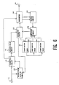
- Fig. 6 is a block diagram of another embodiment of an encoding device according to the present invention.
- the encoding device of Fig. 6 comprises an input terminal 11, an initial value updating circuit 12, a subtraction circuit 13, an absolute value circuit 14, three quantization tables 61, 62 and 63, a comparison circuit 16, a transmitter 66, a switching circuit 64, a monitor circuit 65, and an output terminal 18.
- Applied to the input terminal 11 is a series of image or audio data after being subjected to sampling and quantizing.
- an initial value Si is held in the initial value updating circuit 12.
- the initial value S i is also supplied to the transmitter 17.
- the absolute value circuit 14 calculates an absolute value
- the quantization tables 61, 62 and 63 output the respective threshold values of first quantization scales and supply them to the switching circuit 64.
- the switching circuit 64 selects and outputs a proper input dependent on the output of the monitor circuit 65.
- the comparison circuit 16 compares the threshold value of the selected quantization table with the absolute value
- ⁇ S2 is processed in a like manner to ⁇ S1 through the above-mentioned steps.
- the transmitter 66 supplies respective values of input rate and output rate to the monitor circuit 65.
- the monitor circuit 65 calculates the integrated value of differences between the input rate and the output rate, and converts it to a switching signal which is delivered to the switching circuit 64.
- This embodiment has a function to maintain constant the data output rate of the encoding device.
- the quantization tables 61, 62 and 63 have their quantization scales made up such that when those three quantization tables are used for the same input signal, the first quantization table 61 produces the largest amount of decoded data, the third quantization table 63 produces the least amount of decoded data, and the second quan tization table 62 produces the intermediate amount of decoded data.
- the monitor circuit 65 integrates the difference between the input rate and the output rate at all time, and converts the integrated value to the switching signal.
- the switching circuit 64 When the input rate exceeds the output rate in this stage, the switching circuit 64 outputs such a selection signal as by which the second quantization table 62 is selected. When the input rate still yet exceeds the output rate, another selection signal is output to select the third quantization table 63. To the contrary, when the input rate is below the output rate, the switching circuit 64 is controlled to sequentially select the third quantization table 63, second quantization table 62 and first quantization table 61 in this order. This prevents the encoding device from coming into crash, while keeping the output rate kept at constant.
- Fig. 7 is a more detailed block diagram of the quantization tables 61, 62 and 63, switching circuit 64, monitor circuit 65, and transmitter 66 of Fig. 6.
- the first quantization table 61 comprises a ROM 71 and a counter 72.
- the second quantization table 62 comprises a ROM 73, and the third quantization table 63 comprises a ROM 74.
- the counter 72 is counted up by signal sampling clocks, and reset by the comparison circuit 16 when it detects a matching quantization level.
- the ROM's 71, 73 and 74 are operated synchronously by virtue of the counter 72.
- the switching circuit 64 makes switching action to select any one of the threshold value outputs from the ROM's 71, 73 and 74, and then delivers the selected one to the comparison circuit 16.
- the transmitter 66 comprises a RAM (Random Access Memory) 75, an arbitration circuit 76, a write address counter 77,and a read address counter 78.
- the input data such as index is written into the RAM 75.
- write addresses are produced by the write address counter 77 and applied to the RAM 75 via the arbitration circuit 76.
- read addresses are produced by the read address counter 78 and applied to the RAM 75 via the arbitration circuit 76. Since the transmitter 66 is set to have the constant output rate, the arbitration circuit 76 passes the read addresses with higher priority, while keeping the write addresses queued.
- the monitor circuit 65 comprises a subtractor 79, an accumulator 80 and a converter 81.
- the subtractor 79 subtracts the count value of the read address counter 78 from the count value of the write address counter 77, and then supplies the resulting difference to the accumulator 80.
- the accumulator 80 accumulates the differences about a predetermined value. The increased input rate advances the write address, which reduces the output value of the subtractor 79 so that the output value of the accumulator 80 becomes small.
- the converter 81 produces switching signals by which the switching circuit 64 selects the ROM 74 when the accumulator 80 has a small value, it selects the ROM 73 when the accumulator 80 has a value exceeding a first predetermined threshold value, and it selects the ROM 71 when the accumulator 80 has a value exceeding a second predetermined threshold value. This implements to effect such control as reducing the amount of index and sign data produced when the data input to the RAM 75 is increased, but increasing the amount of index and sign data produced when the data input to the RAM 75 is reduced.
- the monitor circuit and the transmitter in this embodiment are not limited to the illustrated configurations.
- the RAM 75 in the transmitter 66 may comprise a FIFO (First In First Out) memory.
Landscapes
- Engineering & Computer Science (AREA)
- Multimedia (AREA)
- Signal Processing (AREA)
- Theoretical Computer Science (AREA)
- Compression, Expansion, Code Conversion, And Decoders (AREA)
- Compression Or Coding Systems Of Tv Signals (AREA)
Abstract
Description
- The present invention relates to an encoding and decoding method and device for compression encoding, transmitting and decoding of information of an image signal or audio signal.
- In the field of image or voice communication, there has so far been performed compression of signals or highly efficient encoding of data in order to efficiently utilize the limited line capacity. One practical example is an encoding and decoding device for used in TV conference or TV telephone.
- "A Fractal Based Approach to Image Compression", ICASSP, 86, 11A.3 is known to the present inventors as a reference closely related to the present invention. This reference is to compress image data using the fractal concept. The basic concept is in that "yard stick" of certain fixed length is used as a unit to cover a signal, and a horizontal distance of the cross point at which "yard stick" intersects the signal, i.e., sampling interval and a positive or negative sign bit respectively indicative of increase or reduction in an amplitude value are both transmitted for restoration of the signal at the decoding side. The practically implementing method employs "trigger function" in place of "yard stick", the trigger function being compared with the signal to determine a sampling interval. This makes the sampling interval wider for signal including many flat parts, so that the signal may be compressed to a large extent.
- However, because "trigger function" is a unique function for all of successive data samples, the above method cannot follow a multi-value graded image including steeply changing parts, resulting in a problem that the image may be blurry in its edges. Another problem is in that since representative values used in the decoding step are given by those threshold values which were used in the encoding step, the decoded values are always less than the amplitude values of the original signal, and hence the mean square error is increased. It is to be noted that the above reference teaches only the method, and does not propose a practical device.
- It is an object of the present invention to provide a method and device for encoding and decoding signals, which are fit for human visual and auditory characteris tics, and which are adapted to reduce the information content necessary for transmitting and storing an image or audio signal.
- To achieve the above object, the present invention resides in a method of encoding and decoding image and audio signals, any of the signals being subjected to sampling and having a multiplicity of sampling points each represented by a quantized amplitude value.
- An encoding step comprises the steps of:
transmitting an amplitude value of a given sampling point as an initial value;
subtracting the initial value from each of amplitude values of n sampling points (where n is a predetermined integer) to calculate n difference values therebetween, and calculating positive or negative signs, which respectively indicate varying directions of the amplitudes imposed by the difference values with respect to the initial value and absolute values of the difference values ;
previously preparing a quantization table which has threshold values and representative values expressed in terms of amplitude values, defines an ordered set of n quantization scales (where n is a predetermined integer) each comprising at least one threshold value and a repre sentative value, and also defines index values different from one another for all the representative values of said n quantization scales ;
comparing a series of n difference absolute values with a series of n quantization scales included in the quantization table sequentially from the sampling point adjacent to the initial value until the maximum n-th sampling point, and selecting a representative value of the most suitable quantization scale ;
transmitting the index value of the selected representative value of the quantization scale and the positive or negative sign ;and
repeating the foregoing steps with the sum of the selected representative value of the quantization scale and the current initial value being set as a subsequent initial value . - A decoding step comprises the steps of:
receiving the amplitude value of the transmitted sampling point as an initial value ;
previously preparing the same quantization table as used during the encoding step ;
determining the number m and the representative value corresponding to the received index value and the sign by making use of the quantization table ;
interpolating the amplitude value of each of (m-1) sampling points between the initial value and the sum of the initial value and the representative value of m-th sampling point ; and
repeating the foregoing steps with the sum of the initial value and the representative value of m-th sampling point being set as a subsequent initial value. - The foregoing method allows sampling to be finely carried out in the steeply changing part, but roughly carried out in the moderately changing part, so that image and audio signals can be encoded with high efficiency in better fitting for human visual and auditory characteristics.
- Fig. 1 is a block diagram of one embodiment of an encoding device for encoding signals according to the method of the present invention;
- Fig. 2 is a more detailed block diagram of Fig. 1;
- Fig. 3 is one example of quantization table;
- Fig. 4 is a block diagram of one embodiment of a decoding device for decoding the encoded data according to the method of the present invention;
- Fig. 5 is a more detailed block diagram of Fig. 4;
- Fig. 6 is a block diagram of another embodiment of an encoding device for encoding signals according to the method of the present invention; and
- Fig. 7 is a more detailed block diagram of Fig. 6.
- One embodiment of the present invention will be described below with reference to the drawings.
- Fig. 1 is a block diagram of one embodiment of an encoding device according to the present invention. The encoding device of Fig. 1 comprises an
input terminal 11, an initialvalue updating circuit 12, asubtraction circuit 13, anabsolute value circuit 14, a quantization table 15, acomparison circuit 16, atransmitter 17, and anoutput terminal 18. Applied to theinput terminal 11 is a series of image or audio data after being subjected to sampling and quantizing. First, an initial value Si is held in the initialvalue updating circuit 12. The initial value Si is also supplied to thetransmitter 17. The subsequent data Si+1 and the output Si of the initialvalue updating circuit 12 are supplied to asubtraction circuit 13 where both Δ S1 = Si+1 - Si and the sign F1 = sign(ΔS1) are calculated. The output Δ S1 of thesubtraction circuit 13 is then supplied to theabsolute value circuit 14, while F1 is held therein until receiving of an indication from thecomparison circuit 16. Theabsolute value circuit 14 calculates an absolute value | Δ S1 | of Δ S1 and sends it to thecomparison circuit 16. The quantization table 15 is a table having an ordered set of n quantization scales (where n is a positive integer). Each quantization scale has at least one quantization level, and each quantization level has a single representative value Rk. The quantization levels are partitioned from each other by respective threshold values. The quantization table 15 outputs the threshold value of first quantization scale and sends it to thecomparison circuit 16. Thecomparison circuit 16 compares the threshold value of first quantization scale with the absolute value | Δ S1 | to check to which quantization level the absolute value | Δ S1 | belongs. If | Δ S1 | is found within the threshold value of any quantization level, this means the presence of a matching quantization level. In this case, thecomparison circuit 16 supplies the index of quantization level and the sign F1 delivered from thesubtraction circuit 13 to thetransmitter 17. Thecomparison circuit 16 also resets the quantization table 15. Further, thecomparison circuit 16 sends the representative value Rk of the selected index to the initialvalue updating circuit 12. The initialvalue updating circuit 12 holds the sum of the initial value Si originally held therein and the representative value Rk as a new initial value. The above process is effected when the matching quantization level is present. - If the absolute value | Δ S1 | is less than the minimum threshold value of first quantization scale, this means the absence of a matching quantization level. In this case, the subsequent data Si+2 is supplied to the
subtraction circuit 13 where ΔS2 = Si+2 - Si is calculated. ΔS2 is processed in a like manner to ΔS1. More specifically, the quantization table 15 outputs the threshold value of second quantization scale, which is then compared with | Δ S2 | in thecomparison circuit 16. If a matching quantization level is found, thecomparison circuit 16 supplies both the index of that quantization level and the sign delivered from thesubtraction circuit 13. if not, the subsequent sampling point Si+3 is supplied to thesubtraction circuit 13 where ΔS3 = Si+3 - Si is calculated. Thereafter, the similar process will be repeated until calculation of ΔSn = Si+n - Si at maximum. Thetransmitter 17 outputs a series of indices and signs from theoutput terminal 18. - Fig. 2 is a more detailed block diagram of Fig. 1. The initial
value updating circuit 12 comprises aselector 21, register 22 andfull adder 23. Theselector 21 makes switching action to select either the first initial value or the updated initial value. The initial value means, for example, an amplitude value of first pixel on one horizontal scanning line in connection with image. The register 22 holds the initial value selected by theselector 21. Thefull adder 23 adds the current initial value held in theregister 21 and the representative value Rk of the index selected by thecomparison circuit 16, and then outputs the sum therefrom. - The
subtraction circuit 13 comprises a two'scomplementer 24 and afull adder 25. The two'scomplementer 24 operates to determine the subtractive value of the data applied thereto for implementing the subtraction in thefull adder 25. Thefull adder 25 adds the initial values held in the register 22 and the output of the two'scomplementer 24 to thereby obtain the resulting difference value Δ S1. At the same time, the positive or negative sign F1 is also obtained. Theabsolute value circuit 14 functions to determine | Δ S1 | . - The quantization table 15 comprises a ROM (Read Only Memory) 27 for storing threshold values and a
counter 28. Thecounter 28 is reset by thecomparison circuit 16 upon updating of the initial value, and then counted up by sampling clocks applied thereto. Fig. 3 shows the relationship among the index, the sample number, the range of threshold values, and the representative value. TheROM 27 is designed to receive the output of thecoun ter 28, i.e., the sample number, as an address input and responsively output the lowest value of each range of threshold values. Assuming for the sample S1 to be input, for example, thecounter 28outputs 1 as the sample number and supplies it to theROM 27 as an address for accessing. TheROM 27 outputs three values, i.e., 16, 27 and 42 as seen from Fig. 3, and supplies thevalue 16 to acomparator 29, thevalue 27 to acomparator 30, and thevalue 42 to acomparator 31, respectively, the comparators 29-31 being constituent components of thecomparison circuit 16. The output of theabsolute value circuit 14 is supplied to each of thecomparators absolute value circuit 14 is equal to or greater than the output of theROM 27, one or more of the correspondingcomparators absolute value circuit 14 outputting 16- 26, only thecomparator 29 issues a "true" output. With theabsolute value circuit 14 outputting 27 -41, thecomparators absolute value circuit 14 outputting 42 or more, all of thecomparators absolute value circuit 14 is equal to 20, for example, only thecomparator 29 issues a "true" output, while the remaining comparators issue "false" outputs. - A
ROM 32 is designed to output an index, a representative value, and a reset signal for thecounter 28 by making use of the true/false outputs of thecomparators counter 28 as respective address inputs. In case of the foregoing example, since the counter 28 issues the output of 1 and the range of threshold values is 16 - 26, i.e., thecomparator 29 issues a "true" output and thecomparators ROM 32 delivers theindex 1 and therepresentative value 21 as shown in Fig. 3. TheROM 32 outputs a reset signal and supplies it to thecounter 28, when at least one of thecomparators counter 28 is reset in the above case. Supposing that the output of theabsolute value circuit 14 is equal to or less than 15 in the foregoing example, all of thecomparators value updating circuit 12,subtraction circuit 13 andabsolute value circuit 14 operate in a like manner to the above, and theabsolute value circuit 14 outputs | Δ S2 | , Thecounter 28 is counted up and issues the output of 2. Accordingly, theROM 27 now outputs 8 and 17 to thecomparators sample number 5, theROM 32 outputs theindex 7 and therepresentative value 0 irrespective of the output value of theabsolute value circuit 14. The index in the output of theROM 32 is supplied to a register 33 constituting thetransmitter 17, and then delivered from theoutput terminal 18 together with the sign supplied from thefull adder 25. The representative value in the output of theROM 32 is supplied to thefull adder 23. - While the present invention has been described with reference to the quantization table shown in Fig. 3 by way of example, the quantization table is not limited to the illustrated one. Thus, the number of indices, the magnitude of sample numbers, the ranges of threshold values, and representative values may have optional values so long as they will not be contradictory to each other. Therefore, the number of comparators to be included in the
comparison circuit 16 depends on the con figuration of each quantization table. - With the operation as mentioned above, the part of signal which has an amplitude value changing steeply is quantized at the first sample, but the sample number proceeds in order of 2, 3, 4 and 5 as the signal changes more moderately. As a result, the original sampling interval is widened and hence the amount of data is reduced. Generally speaking, since the natural image or audio signal has many moderately changing parts as a whole, the present method makes it possible to increase the compression rate.
- Fig. 4 shows one embodiment of a decoding device according to the present invention. The decoding device of Fig. 4 comprises an
input terminal 41, areceiver 42, a quantization table 43, aninterpolation circuit 44, anarithmetic circuit 45, an initialvalue updating circuit 46, and anoutput terminal 47. A series of encoded data as inputted to theinput terminal 41 and then supplied to thereceiver 42. Thereceiver 42 separates the initial value Si from the index k and the sign F. The initial value is supplied to the initialvalue updating circuit 46, and the index and the sign are supplied to the quantization table 43. the quantization table 43 has the same quantization table as used in the encoding device, and outputs the sample number and the representative value upon receiving the index applied thereto. The representative value is added with the positive or negative sign and then supplied to theinterporation circuit 44. Theinterpolation circuit 44 calculates one or more interpolation values from the sample number and the representative value. The case ofsample number 1 does not require interpolation, but the case ofsample number 2 or more requires interpolation. The interpolated data is in the form of series of difference values and supplied to thearithmetic circuit 45. In thearithmetic circuit 45, the initial value held in the initialvalue updating circuit 46 and the series of difference values are sequentially added to give a series of decoded signals, which is then delivered from theoutput terminal 47. The final value in the data series from thearithmetic circuit 45 is supplied to the initialvalue updating circuit 46 for updating the previous initial value. - Fig. 5 is a more detailed block diagram of Fig. 4. The
receiver 42 comprises aregister 51. Theregister 51 separates the initial value out of the data series encoded by the encoding device, followed by supplying it to the initialvalue updating circuit 46, while it supplies the index and the sign to the quantization table 43. - The quantization table 43 comprises a
ROM 52. TheROM 52 outputs the sample number and the representative value using the index and the sign as address inputs. If the encoding device employs the quantization table shown in Fig. 3, the decoding device has also to employ the same quantization table as shown in Fig. 3. The representative value output from theROM 52 is given by the representative value shown in Fig. 3 added with the positive or negative sign. - The
interpolation circuit 44 comprises a down counter 53 and aROM 54. The sample number outputted from theROM 52 is loaded into the down counter 53. The representative value delivered from theROM 54 and the output of the down counter 53 are supplied to aROM 54 as addresses for accessing. Responsively, theROM 54 outputs the interpolation value which is previously calculated and stored therein. - The
arithmetic circuit 45 comprises afull adder 55. Thefull adder 55 adds the output of theROM 54 and the initial value stored in aregister 57 of the initialvalue updating circuit 46, and then supplies the resulting sum to theoutput terminal 47. Aselector 56 of the initialvalue updating circuit 46 makes switching action to selects either the initial value supplied from theregister 51 or the final output value from thefull adder 55. Only upon theregister 51 detecting the initial value, theselector 56 is switched to the side of theregister 51. The output of theselector 56 is supplied to theregister 57. The new initial value is stored in theregister 57 and, at the same time, theregister 51 supplies the subsequent index and sign to theROM 52 for repeating the above process. - While both the index and the sign were employed as input addresses for the ROM storing the quantization table in the foregoing embodiment, it may be configured that only the index is employed as an input address for the ROM, and the sign is directly added to the output of the ROM for providing the representative value with the positive or negative sign. Also, while the interpolation circuit was consisted of the down counter and the ROM, it is not limited to such configuration and may comprise, for example, an up counter, a comparator and a ROM.
- Fig. 6 is a block diagram of another embodiment of an encoding device according to the present invention. The encoding device of Fig. 6 comprises an
input terminal 11, an initialvalue updating circuit 12, asubtraction circuit 13, anabsolute value circuit 14, three quantization tables 61, 62 and 63, acomparison circuit 16, atransmitter 66, a switchingcircuit 64, amonitor circuit 65, and anoutput terminal 18. Applied to theinput terminal 11 is a series of image or audio data after being subjected to sampling and quantizing. First, an initial value Si is held in the initialvalue updating circuit 12. The initial value Si is also supplied to thetransmitter 17. The subsequent data Si+1 and the output Si of the initialvalue updating circuit 12 are supplied to asubtraction circuit 13 where both ΔS1 = Si+1 - Si and the sign F1 = sign(ΔS1) are calculated. Then, the output ΔS1 of thesubtraction circuit 13 is supplied to theabsolute value circuit 14, and F1 is supplied to thetransmitter 66. Theabsolute value circuit 14 calculates an absolute value | Δ S1 | of ΔS1 and sends it to thecomparison circuit 16. On the other hand, the quantization tables 61, 62 and 63 output the respective threshold values of first quantization scales and supply them to the switchingcircuit 64. The switchingcircuit 64 selects and outputs a proper input dependent on the output of themonitor circuit 65. Thecomparison circuit 16 compares the threshold value of the selected quantization table with the absolute value | Δ S1 | to check to which quantization level the absolute value |ΔS1| belongs. If a matching quantization level is found, thecomparison circuit 16 supplies the index of quantization level to thetransmitter 66. Concurrently, the sign F1 is supplied from thesubtraction circuit 13 to thetransmitter 66. Further, the representative value Rk of the selected index is supplied to the initialvalue updating circuit 12. The initialvalue updating circuit 12 updates the sum of the initial value Si originally held therein and the representative value Rk as a new initial value. - If the absolute value | Δ S1 | is less than the minimum threshold value of quantization scale for the first sample, the matching quantization level cannot be found. Thus, the subsequent data Si+2 is supplied to the
subtraction circuit 13 where ΔS2 = Si+2 - Si is calculated. ΔS2 is processed in a like manner to ΔS1 through the above-mentioned steps. Thetransmitter 66 supplies respective values of input rate and output rate to themonitor circuit 65. Themonitor circuit 65 calculates the integrated value of differences between the input rate and the output rate, and converts it to a switching signal which is delivered to the switchingcircuit 64. - This embodiment has a function to maintain constant the data output rate of the encoding device. The quantization tables 61, 62 and 63 have their quantization scales made up such that when those three quantization tables are used for the same input signal, the first quantization table 61 produces the largest amount of decoded data, the third quantization table 63 produces the least amount of decoded data, and the second quan tization table 62 produces the intermediate amount of decoded data. Provided that the input data rate is higher than the output data rate owing to the complicated input signal, the transmission will soon be crashed. To avoid such crash, the
monitor circuit 65 integrates the difference between the input rate and the output rate at all time, and converts the integrated value to the switching signal. It is assumed that the first quantization table 61 is selected by the switchingcircuit 64 at the first stage. When the input rate exceeds the output rate in this stage, the switchingcircuit 64 outputs such a selection signal as by which the second quantization table 62 is selected. When the input rate still yet exceeds the output rate, another selection signal is output to select the third quantization table 63. To the contrary, when the input rate is below the output rate, the switchingcircuit 64 is controlled to sequentially select the third quantization table 63, second quantization table 62 and first quantization table 61 in this order. This prevents the encoding device from coming into crash, while keeping the output rate kept at constant. - Fig. 7 is a more detailed block diagram of the quantization tables 61, 62 and 63, switching
circuit 64,monitor circuit 65, andtransmitter 66 of Fig. 6. The first quantization table 61 comprises a ROM 71 and acounter 72. The second quantization table 62 comprises a ROM 73, and the third quantization table 63 comprises a ROM 74. Thecounter 72 is counted up by signal sampling clocks, and reset by thecomparison circuit 16 when it detects a matching quantization level. The ROM's 71, 73 and 74 are operated synchronously by virtue of thecounter 72. The switchingcircuit 64 makes switching action to select any one of the threshold value outputs from the ROM's 71, 73 and 74, and then delivers the selected one to thecomparison circuit 16. - The
transmitter 66 comprises a RAM (Random Access Memory) 75, anarbitration circuit 76, awrite address counter 77,and aread address counter 78. The input data such as index is written into theRAM 75. At this time, write addresses are produced by thewrite address counter 77 and applied to theRAM 75 via thearbitration circuit 76. Meanwhile, read addresses are produced by the readaddress counter 78 and applied to theRAM 75 via thearbitration circuit 76. Since thetransmitter 66 is set to have the constant output rate, thearbitration circuit 76 passes the read addresses with higher priority, while keeping the write addresses queued. - The
monitor circuit 65 comprises a subtractor 79, an accumulator 80 and aconverter 81. The subtractor 79 subtracts the count value of the read address counter 78 from the count value of thewrite address counter 77, and then supplies the resulting difference to the accumulator 80. The accumulator 80 accumulates the differences about a predetermined value. The increased input rate advances the write address, which reduces the output value of the subtractor 79 so that the output value of the accumulator 80 becomes small. Theconverter 81 produces switching signals by which theswitching circuit 64 selects the ROM 74 when the accumulator 80 has a small value, it selects the ROM 73 when the accumulator 80 has a value exceeding a first predetermined threshold value, and it selects the ROM 71 when the accumulator 80 has a value exceeding a second predetermined threshold value. This implements to effect such control as reducing the amount of index and sign data produced when the data input to theRAM 75 is increased, but increasing the amount of index and sign data produced when the data input to theRAM 75 is reduced. - The monitor circuit and the transmitter in this embodiment are not limited to the illustrated configurations. For example, the
RAM 75 in thetransmitter 66 may comprise a FIFO (First In First Out) memory.
Claims (7)
an encoding step comprising the substeps of:
transmitting an amplitude value of a given sampling point as an initial value ;
subtracting said initial value from an amplitude value of an m-th sampling point counting from the initial sampling point to calculate a difference value therebetween, where m is an integer larger than 1 but smaller than a predetermined integer n , and calculating a positive or negative sign which indicates a varying direction of the amplitude imposed by said difference value with respect to said initial value and an absolute value of said difference value ;
previously preparing a quantization table which has threshold values and representative values expressed in terms of amplitude values, defines an ordered set of n quantization scales each comprising at least one threshold value and a representative value, and also defines index values different from one another for each representative value of said n quantization scales;
comparing said m-th difference absolute value with the m-th quantization scale in a series of n quantization scales included in said quantization table sequentially from m = 1 to m = n, and selecting a representative value of the most suitable quantization scale;
transmitting the index value of said selected representative value of the quantization scale and said positive or negative sign ;and
repeating the foregoing substeps with the sum of said selected representative value of the quantization scale and the current initial value being set as a subsequent initial value; and
a decoding step comprising the substeps of :
receiving an amplitude value of the transmitted sampling point as an initial value ;
previously preparing the same quantization table as that used during the encoding step ;
determining the number m and the representative value corresponding to the received index value and the sign by making use of said quantization table ;
interpolating the amplitude value of each of (m-1) sampling points between said initial value and the sum of said initial value and the representative value of m-th sampling point ;and
repeating the foregoing substeps with the sum of said initial value and the representative value of m-th sampling point being set as a subsequent initial value.
transmitting an amplitude value of a given sampling point as an initial value;
subtracting said initial value from an amplitude value of an m-th sampling point counting from the initial sampling point to calculate a difference value therebetween , where m is an integer larger than 1 but smaller than a predetermined integer n , and calculating a positive or negative sign which indicates a varying direction of the amplitude imposed by said difference value with respect to said initial value, and an absolute value of said difference value ;
previously preparing a quantization table which includes threshold values and representative values expressed in terms of amplitude values, defines an ordered set of n quantization scales each comprising at least one threshold value and a representative value, and also defines index values different from one another for each representative value of said n quantization scales ;
comparing said m-th difference absolute value with the m-th quantization scale in a series of n quantization scales included in said quantization table sequentially from m = 1 to m = n, and selecting a representative value of the most suitable quantization scale;
transmitting the index value of said selected representative value of the quantization scale and said positive or negative sign; and
repeating the foregoing steps with the sum of said selected representative value of the quantization scale and the current initial value being set as a subsequent initial value.
means for calculating a difference value ΔSm = Si+m - Si between an initial value Si and a succeeding sample signal Si+m (m = 1, 2,...), assuming the initial value of sampling series ..., Si-1, Si, Si+1, ... of an input signal to be Si ;
means for calculating an absolute value | Δ Sm | of said difference value ΔSm and a sign Fm ;
a quantization table which includes threshold values and representative values expressed in terms of amplitude values, defines an ordered set of predetermined n quantization scales each comprising at least one threshold value and a representative value Rk, and also defines index values k different from one another for each representative value of said n quantization scales ;
comparison means for comparing said absolute value | Δ Sm | with the threshold value of m-th quantization scale included in said quantization table sequentially, and selecting and outputting the index value k corresponding to the most suitable quantization scale;
means for advancing the sample number i of said initial value Si of the input signal in response to the output from said comparison circuit by m until i+m, and replacing said initial value Si with Si+m = Si + Rk; and
means for transmitting a series of data comprising said index values k and the corresponding signs Fm, as well as said initial value Si.
means for receiving and separating index values k, signs Fm and an initial value Si transmitted from said encoding apparatus;
a quantization table adapted to output the same quantized representative values as those in said encoding apparatus for respective sample number values corresponding to said index values k;
means for adding said initial value Si to the product of said quantized representative value and said sign Fm;
interpolation processing means for interpolating (m-1) samples between said initial value Si and the sampling point spaced therefrom by m samples; and
initial value updating means for loading the output of said adding means in said initial value updating means as a subsequent initial value.
means for calculating a difference value ΔSm = Si+m - Si between an initial value Si and a succeeding sample signal Si+m (m = 1, 2,...), assuming the initial value of sampling series S₀, S₁,..., Si, Si+1, ... of an input signal to be Si;
means for calculating an absolute value | Δ Sm | of said difference value ΔSm and a sign Fm ;
a first quantization table which includes threshold values and representative values expressed in terms of amplitude values, defines an ordered set of predetermined n quantization scales each comprising at least one threshold value and a representative value Rk, and also defines index values k different from one another for each representative value of said n quantization scales ;
at least one additional quantization table having quantization scales different from those in said first quantization table ;
means for selecting a threshold value of any one of said plurality of quantization tables ;
comparison means for comparing said absolute value | Δ Sm | with the threshold value of any one of said quantization tables selected by said selection means, and selecting and outputting the index value k corresponding to the most suitable quantization scale;
means for advancing the sample number i of said ini tial value Si of the input signal in response to the output from said comparison circuit by m until i+m, and replacing said initial value Si with Si+m = Si + Rk;
transmitting a series of data comprising said index values k and the corresponding signs Fm, as well as said initial value Si at a constant rate; and
data rate monitor means for monitoring the input data rate and the output data rate of said transmission means at all times, and controlling said selection means based on the monitoring result.
Applications Claiming Priority (6)
| Application Number | Priority Date | Filing Date | Title |
|---|---|---|---|
| JP181520/87 | 1987-07-21 | ||
| JP62181520A JPS6424687A (en) | 1987-07-21 | 1987-07-21 | Image encoder |
| JP62236526A JPS6478589A (en) | 1987-09-21 | 1987-09-21 | Picture decoder |
| JP236526/87 | 1987-09-21 | ||
| JP62309922A JPH01151384A (en) | 1987-12-08 | 1987-12-08 | Picture coding device |
| JP309922/87 | 1987-12-08 |
Publications (3)
| Publication Number | Publication Date |
|---|---|
| EP0300775A2 true EP0300775A2 (en) | 1989-01-25 |
| EP0300775A3 EP0300775A3 (en) | 1991-01-16 |
| EP0300775B1 EP0300775B1 (en) | 1995-05-31 |
Family
ID=27325021
Family Applications (1)
| Application Number | Title | Priority Date | Filing Date |
|---|---|---|---|
| EP88306679A Expired - Lifetime EP0300775B1 (en) | 1987-07-21 | 1988-07-20 | Signal encoding and decoding method and device |
Country Status (4)
| Country | Link |
|---|---|
| US (1) | US4953214A (en) |
| EP (1) | EP0300775B1 (en) |
| KR (1) | KR920003860B1 (en) |
| DE (1) | DE3853899T2 (en) |
Cited By (3)
| Publication number | Priority date | Publication date | Assignee | Title |
|---|---|---|---|---|
| EP0784312A3 (en) * | 1996-01-10 | 1998-09-23 | Nec Corporation | Encoding system and decoding system for audio signals |
| WO2000041314A1 (en) * | 1998-12-31 | 2000-07-13 | Samsung Electronics Co., Ltd. | Quantization method for iterative decoder in communication system |
| US10467823B2 (en) | 2015-11-20 | 2019-11-05 | Samsung Electronics Co., Ltd. | Apparatus and method for transmitting and receiving data |
Families Citing this family (18)
| Publication number | Priority date | Publication date | Assignee | Title |
|---|---|---|---|---|
| USRE40280E1 (en) | 1988-12-30 | 2008-04-29 | Lucent Technologies Inc. | Rate loop processor for perceptual encoder/decoder |
| US5230038A (en) * | 1989-01-27 | 1993-07-20 | Fielder Louis D | Low bit rate transform coder, decoder, and encoder/decoder for high-quality audio |
| US5388181A (en) * | 1990-05-29 | 1995-02-07 | Anderson; David J. | Digital audio compression system |
| US6915014B1 (en) | 1990-07-31 | 2005-07-05 | Canon Kabushiki Kaisha | Image processing apparatus and method |
| EP0469835B1 (en) * | 1990-07-31 | 1998-09-30 | Canon Kabushiki Kaisha | Image processing apparatus and method |
| EP0559348A3 (en) * | 1992-03-02 | 1993-11-03 | AT&T Corp. | Rate control loop processor for perceptual encoder/decoder |
| US6100933A (en) * | 1994-10-31 | 2000-08-08 | Intel Corporation | Process and apparatus for compressing and decompressing digital video signals using horizontally-based vector quantization |
| US5862263A (en) * | 1995-04-13 | 1999-01-19 | Samsung Electronics Co., Ltd. | Fractal image compression device and method using perceptual distortion measurement |
| KR0154739B1 (en) * | 1995-04-19 | 1998-11-16 | 김광호 | Fractal image compression device and method |
| US5822721A (en) * | 1995-12-22 | 1998-10-13 | Iterated Systems, Inc. | Method and apparatus for fractal-excited linear predictive coding of digital signals |
| US5831559A (en) * | 1996-01-24 | 1998-11-03 | Intel Corporation | Encoding/decoding video signals using multiple run-val mapping tables |
| US5913186A (en) * | 1996-03-25 | 1999-06-15 | Prometheus, Inc. | Discrete one dimensional signal processing apparatus and method using energy spreading coding |
| JP2000506687A (en) * | 1996-03-29 | 2000-05-30 | サーノフ コーポレイション | Apparatus and method for optimizing encoding using perceptual amount and performing automatically operable image compression |
| US6295379B1 (en) * | 1997-09-29 | 2001-09-25 | Intel Corporation | DPCM image compression with plural quantization table levels |
| US6459392B1 (en) | 2001-01-19 | 2002-10-01 | International Business Machines Corporation | Technique for encoding a sequence of periodic byte values with vertical correlation |
| SE0402651D0 (en) * | 2004-11-02 | 2004-11-02 | Coding Tech Ab | Advanced methods for interpolation and parameter signaling |
| GB2451828A (en) * | 2007-08-13 | 2009-02-18 | Snell & Wilcox Ltd | Digital audio processing method for identifying periods in which samples may be deleted or repeated unobtrusively |
| WO2010074259A1 (en) | 2008-12-26 | 2010-07-01 | 旭化成せんい株式会社 | Extensible optical sugnal transmission cable |
Citations (2)
| Publication number | Priority date | Publication date | Assignee | Title |
|---|---|---|---|---|
| US4093962A (en) * | 1976-12-01 | 1978-06-06 | Nippon Electric Co., Ltd. | Adaptive predictive encoder |
| FR2569074A1 (en) * | 1984-04-25 | 1986-02-14 | Matsushita Electric Works Ltd | METHOD AND SYSTEM FOR IMAGE TRANSMISSION |
Family Cites Families (2)
| Publication number | Priority date | Publication date | Assignee | Title |
|---|---|---|---|---|
| US4802222A (en) * | 1983-12-12 | 1989-01-31 | Sri International | Data compression system and method for audio signals |
| US4670851A (en) * | 1984-01-09 | 1987-06-02 | Mitsubishi Denki Kabushiki Kaisha | Vector quantizer |
-
1988
- 1988-07-20 DE DE3853899T patent/DE3853899T2/en not_active Expired - Fee Related
- 1988-07-20 EP EP88306679A patent/EP0300775B1/en not_active Expired - Lifetime
- 1988-07-21 KR KR1019880009095A patent/KR920003860B1/en not_active IP Right Cessation
- 1988-07-21 US US07/222,171 patent/US4953214A/en not_active Expired - Fee Related
Patent Citations (2)
| Publication number | Priority date | Publication date | Assignee | Title |
|---|---|---|---|---|
| US4093962A (en) * | 1976-12-01 | 1978-06-06 | Nippon Electric Co., Ltd. | Adaptive predictive encoder |
| FR2569074A1 (en) * | 1984-04-25 | 1986-02-14 | Matsushita Electric Works Ltd | METHOD AND SYSTEM FOR IMAGE TRANSMISSION |
Non-Patent Citations (2)
| Title |
|---|
| ELECTRONICS AND COMMUNICATIONS IN JAPAN, vol. 58-A, no. 2, 1975, pages 11-20, New York, US; T. KAWADE et al.: "A variable sampling rate coding technique" * |
| PROCEEDINGS OF THE IEEE, vol. 73, no. 4, April 1985, pages 765-772, New York, US; H. BULEY et al.: "Inter/intraframe coding of color TV signals for transmission at the third level of the digital hierarchy" * |
Cited By (4)
| Publication number | Priority date | Publication date | Assignee | Title |
|---|---|---|---|---|
| EP0784312A3 (en) * | 1996-01-10 | 1998-09-23 | Nec Corporation | Encoding system and decoding system for audio signals |
| WO2000041314A1 (en) * | 1998-12-31 | 2000-07-13 | Samsung Electronics Co., Ltd. | Quantization method for iterative decoder in communication system |
| US6876709B1 (en) | 1998-12-31 | 2005-04-05 | Samsung Electronics Co., Ltd. | Quantization method for iterative decoder in communication system |
| US10467823B2 (en) | 2015-11-20 | 2019-11-05 | Samsung Electronics Co., Ltd. | Apparatus and method for transmitting and receiving data |
Also Published As
| Publication number | Publication date |
|---|---|
| DE3853899T2 (en) | 1995-12-21 |
| US4953214A (en) | 1990-08-28 |
| EP0300775A3 (en) | 1991-01-16 |
| KR890003140A (en) | 1989-04-13 |
| KR920003860B1 (en) | 1992-05-15 |
| DE3853899D1 (en) | 1995-07-06 |
| EP0300775B1 (en) | 1995-05-31 |
Similar Documents
| Publication | Publication Date | Title |
|---|---|---|
| EP0300775A2 (en) | Signal encoding and decoding method and device | |
| JP3017380B2 (en) | Data compression method and apparatus, and data decompression method and apparatus | |
| US5016010A (en) | System for controlling a number of bits required to represent coded output data | |
| US4694336A (en) | Digital data transmission method | |
| JPH0216075B2 (en) | ||
| EP0084270A2 (en) | Video bandwidth reduction system employing interframe block differencing and transform domain coding | |
| EP0737015A2 (en) | Encoding apparatus | |
| EP0249086A2 (en) | Method and apparatus for encoding/transmitting image | |
| EP0402149B1 (en) | Coding device | |
| US5107519A (en) | Coding device and a decoding device | |
| EP1613092A2 (en) | Fixed budget frame buffer compression using block-adaptive spatio-temporal dispersed dither | |
| EP0535272A1 (en) | Hybrid encoder arrangement for an image processing system | |
| JP2911682B2 (en) | Motion compensation using the minimum number of bits per motion block as a criterion for block matching | |
| US6611559B1 (en) | Apparatus and method of detecting motion vectors by calculating a correlation degree between each candidate block | |
| CA2028947C (en) | Picture coding apparatus | |
| EP0633701A2 (en) | Method and device for the compression of a digital video signal | |
| US5905578A (en) | Coding apparatus | |
| US4979187A (en) | Predictive coding device | |
| EP0238254A2 (en) | Data compression using block list transform | |
| EP0599653B1 (en) | Digital sound level control in a telephone system | |
| JPH0669811A (en) | Encoding circuit and decoding circuit | |
| JP2929591B2 (en) | Image coding device | |
| KR910009092B1 (en) | Vector quantum cooling and decoding apparatus | |
| EP0859519A2 (en) | Video coder using implicit or explicit prediction for image coding | |
| EP0609835B1 (en) | Address generation circuit of two-dimensional coding table for Huffman code |
Legal Events
| Date | Code | Title | Description |
|---|---|---|---|
| PUAI | Public reference made under article 153(3) epc to a published international application that has entered the european phase |
Free format text: ORIGINAL CODE: 0009012 |
|
| AK | Designated contracting states |
Kind code of ref document: A2 Designated state(s): DE FR GB |
|
| PUAL | Search report despatched |
Free format text: ORIGINAL CODE: 0009013 |
|
| AK | Designated contracting states |
Kind code of ref document: A3 Designated state(s): DE FR GB |
|
| 17P | Request for examination filed |
Effective date: 19910709 |
|
| 17Q | First examination report despatched |
Effective date: 19930526 |
|
| GRAA | (expected) grant |
Free format text: ORIGINAL CODE: 0009210 |
|
| AK | Designated contracting states |
Kind code of ref document: B1 Designated state(s): DE FR GB |
|
| REF | Corresponds to: |
Ref document number: 3853899 Country of ref document: DE Date of ref document: 19950706 |
|
| PGFP | Annual fee paid to national office [announced via postgrant information from national office to epo] |
Ref country code: GB Payment date: 19950710 Year of fee payment: 8 |
|
| PGFP | Annual fee paid to national office [announced via postgrant information from national office to epo] |
Ref country code: FR Payment date: 19950711 Year of fee payment: 8 |
|
| PGFP | Annual fee paid to national office [announced via postgrant information from national office to epo] |
Ref country code: DE Payment date: 19950725 Year of fee payment: 8 |
|
| ET | Fr: translation filed | ||
| PLBE | No opposition filed within time limit |
Free format text: ORIGINAL CODE: 0009261 |
|
| STAA | Information on the status of an ep patent application or granted ep patent |
Free format text: STATUS: NO OPPOSITION FILED WITHIN TIME LIMIT |
|
| 26N | No opposition filed | ||
| PG25 | Lapsed in a contracting state [announced via postgrant information from national office to epo] |
Ref country code: GB Effective date: 19960720 |
|
| GBPC | Gb: european patent ceased through non-payment of renewal fee |
Effective date: 19960720 |
|
| PG25 | Lapsed in a contracting state [announced via postgrant information from national office to epo] |
Ref country code: FR Effective date: 19970328 |
|
| PG25 | Lapsed in a contracting state [announced via postgrant information from national office to epo] |
Ref country code: DE Effective date: 19970402 |
|
| REG | Reference to a national code |
Ref country code: FR Ref legal event code: ST |