EP0300433B1 - Method for manufacturing bonded semiconductor body - Google Patents
Method for manufacturing bonded semiconductor body Download PDFInfo
- Publication number
- EP0300433B1 EP0300433B1 EP88111617A EP88111617A EP0300433B1 EP 0300433 B1 EP0300433 B1 EP 0300433B1 EP 88111617 A EP88111617 A EP 88111617A EP 88111617 A EP88111617 A EP 88111617A EP 0300433 B1 EP0300433 B1 EP 0300433B1
- Authority
- EP
- European Patent Office
- Prior art keywords
- semiconductor
- semiconductor body
- surface roughness
- bonded
- bonded semiconductor
- Prior art date
- Legal status (The legal status is an assumption and is not a legal conclusion. Google has not performed a legal analysis and makes no representation as to the accuracy of the status listed.)
- Expired - Lifetime
Links
Images


Classifications
-
- H—ELECTRICITY
- H10—SEMICONDUCTOR DEVICES; ELECTRIC SOLID-STATE DEVICES NOT OTHERWISE PROVIDED FOR
- H10P—GENERIC PROCESSES OR APPARATUS FOR THE MANUFACTURE OR TREATMENT OF DEVICES COVERED BY CLASS H10
- H10P10/00—Bonding of wafers, substrates or parts of devices
- H10P10/12—Bonding of semiconductor wafers or semiconductor substrates to semiconductor wafers or semiconductor substrates
- H10P10/128—Bonding of semiconductor wafers or semiconductor substrates to semiconductor wafers or semiconductor substrates by direct semiconductor to semiconductor bonding
Definitions
- This invention relates to a method for manufacturing bonded semiconductor bodies, and more particularly to a method for manufacturing semiconductor bodies by directly bonding silicon substrates together, or directly bonding a substrate of Si, GaAs or other semiconductor material with a substrate of the same material or different semiconductor material.
- pn junctions and heterojunctions which have been considered difficult to form in a prior art can be easily formed in a short period of time.
- the cost will be high when conventional epitaxial method is used, and it takes as long as three to ten days if a triple diffusion method is used.
- the pn junction can be obtained in a period of as short as two hours by directly bonding the n - -type and p - -type layers together.
- the both surfaces of Si substrates 1 and 2, facing at bonding interface 3, are cleaned and polished to make a mirror surface with a surface roughness (maximum height) of less than 500 ⁇ .
- the mirror surfaces are physically brought into contact with each other in a clean atmosphere with no dust, and then the two substrates are subjected to a heat treatment at a temperature of higher than 200°C, normally at a temperature of 1100°C, for two hours in an N 2 gas atmosphere so as to increase the chemical bonding strength between the two substrates (Japanese Patent Disclosure 60-51700 and U.S. Patent Application No. 824,100 which was filed on Jan. 30, 1986 and is now abandoned).
- the bonding strength between the two contacted substrates prior to the heat treatment is approx. 5 kg/cm 2 , but the bonding strength can be increased to 100 kg/cm 2 after the heat treatment.
- the outer surface of the bonded semiconductor body, which is different from the bonded surface, is subjected to rough polishing and finish polishing in this order, and then semiconductor elements and electrodes are formed in and on the bonded semiconductor body in the same manner as in case of using a single semiconductor substrate.
- a bonded semiconductor body (4) having the above-mentioned large bonding strength (100 kg/cm 2 ) can be obtained in a manner that a pair of semiconductor wafers, each having less than 500 ⁇ of a surface roughness and less than 5 ⁇ m of a total thickness variation range for the bonding area, are prepared, and they are contacted with each other in a clean atmosphere condition by which an interference fringe of voids due to dust can be removed.
- the inventor of the present patent application has known that when bonded semiconductor body 4 obtained by the above manner is observed by the infrared topography, dark portions like the surface of the moon or Mars may sometimes be observed, as is shown in Fig. 1A.
- the inventor does not know anyone who has investigated a specific relation between the dark portions as shown in Fig. 1A and defect of the resultant bonded semiconductor body. This is probably because the dark portions like the surface of Mars disappear after suitable heat treatment, as is shown in Fig. 1B and, after such heat treatment, the final product of bonded semiconductor body 4 has a large bonding strength as mentioned above.
- the defect of the bonded semiconductor body can be found after the final product of the bonded semiconductor body, on which many circuit elements are formed, is diced into small pieces or chips.
- Bonded semiconductor body 4 shown in Fig. 1B seems to be non-defective. Many circuit elements are formed on body 4 and then body 4 is diced into small chips (0.5 ⁇ 0.5 mm or 0.5 mm ⁇ ).
- Fig. 1C shows an example of the resultant diced body 4 (observed by photograph, not by infrared topography).
- the vertical and horizontal lines indicate the dicing lines with pitch of 0.5 mm
- the slant lines indicate the defective portions in which parts of bonded 0.5 mm ⁇ chips are peeled off from their bonding interfaces, as is shown in Fig. 1D. Even if such peeling off does not happen, insufficient bonding of the chips causes to abnormally increase the electrical resistance thereof and, therefore, such chips are also defective. In critical cases, bonded semiconductor body 4 itself is cracked and broken during the process of polishing or manufacturing the device (dicing).
- Prior art document EP-A-0 190 935 discloses a method of manufacturing semiconductor devices using a bonding process.
- mirror-polished surfaces of two impurity-doped layers of first and second semiconductor substrates are brought into contact with each other at a temperature of not less than 200°C so as to bond them together.
- the surface roughness of the mirror-polished surface is preferably 500 ⁇ or less, and in the case of an Si substrate, the annealing temperature is preferably 1000°C to 1200°C.
- Another object of this invention is to provide a method for manufacturing bonded semiconductor bodies which can provide substantially uniform image when observed by use of infrared topography.
- the present invention provides a method as specified in claim 1.
- the method for manufacturing bonded semiconductor bodies comprises the steps of bringing the mirror surfaces of semiconductor substrates of the same type or different types, which may be chemical compound semiconductor substrate of GaAs, InP or GaP, silicon substrates and germanium substrates, into close contact with each other; and then subjecting the semiconductor substrates to a heat treatment at a temperature of higher than 200°C to bond the contacted mirror surfaces together.
- the surface roughness of the mirror surfaces of the semiconductor substrates used is set equal to or less than 130 ⁇ in its maximum height for a measured range of 1 mm which is the length defined on a reference plane provided in a predetermined area on the mirror surface.
- the surface roughness is set less than 130 ⁇ in its maximum height for the measured range of 1 mm on the reference plane provided in an area to be observed, dark portions like a sea in the surface of the moon or Mars will not appear in the image observed by use of infrared topography.
- Fig. 2 shows the dependency of the bonding property on the surface roughness. As is clearly seen from Fig. 2, the bonding property is abruptly lowered when the surface roughness exceeds 130 ⁇ (indicated by one-dot-dash line).
- the measured range in the reference plane provided on the surface is set to be 1 mm and set the maximum surface roughness to 130 ⁇ . Further, the total thickness variation (TTV) of the entire surface of the wafer used here is set less than 5 ⁇ m.
- N-type silicon wafers were prepared, each of which has a diameter of 100 mm and the resistivity of 20 to 30 ⁇ cm, each of whose total thickness variation (TTV) is less than 5 ⁇ m, and each of whose surface roughness ranges from 30 ⁇ to 280 ⁇ .
- the measurement of the surface roughness was effected by use of non-bonded surface roughness measuring device, Model "Surfcom 920A" (spot diameter of 1.6 ⁇ m) manufactured by Tokyo Seimitsu Co. Ltd., Japan, and the maximum height was measured in five areas on the wafer with a magnification factor of 1,000,000 and a measurement distance of 1 mm. The average of the measurements was used to determine the surface roughness.
- 500 wafers having the surface roughness of less than 130 ⁇ were selected as one lot from the originally prepared and measured wafers, and 250 sets of contact wafers were formed by respectively contacting together two wafers selected out of the lot.
- the 250 sets of contact wafers were subjected to bonding heat treatment at a temperature of 1100°C (lower than the melting point of the wafer) in an N 2 gas atmosphere (the melting point of the Si wafer is approx. 1400°C).
- Fig. 4 shows the state of void of the bonded wafers of the sample-1 and the comparison sample when observed by means of infrared topography.
- the void in the comparison sample includes void, which is caused by dust and is indicated by interference fringes, and void due to the roughness indicated by dark portions similar to a sea on the moon or Mars.
- the void in the sample-1 includes only void caused by dust and the amount thereof is substantially the same as the comparison sample, and includes no void due to the roughness.
- Fig. 5 is a graph showing the yield of bonded semiconductor bodies with respect to the comparison sample and sample-1, both of which have been subjected to the same device forming process.
- the yield of the sample-1 is higher than that of the comparison sample by 13 %, and it has been determined that the improvement in the yield could be attained because the surface roughness was set less than 130 ⁇ to thereby completely prevent occurrence of crack or breakage of the semiconductor substrates.
- wafers with the roughness of less than 130 ⁇ can be easily available from various wafer makers. Further, complete mirror surface wafers with the surface roughness of 130 ⁇ or less can be obtained by use of the polishing method disclosed in the following Japanese documents:
- the infrared topography is used for observation of the bonding interface.
- JP-A-62-122 141 details the use of infrared rays to observe a bonding interface.
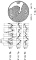
- Fig. 6 shows the bonding condition of a bonded semiconductor substrate wafer (sample A) according to this invention.
- the surface roughness of sample A is less than 130 ⁇ .
- Sample A is diced into 0.5 mm ⁇ pieces, and is observed by use of infrared topography.
- Figs. 6A to 6C show the results of measurement of the surface roughness (92 ⁇ , 124 ⁇ , and 106 ⁇ ) in three preset points in Fig. 6.
- Fig. 6 indicates that no void is observed on the entire surface of the wafer.
- the white ring illustrated at the outer periphery of the disk-like wafer sample A shown in Fig. 6 indicates a non-bonded area.
- the width of such a non-bonded area is generally about 2 mm for the wafer of 100 mm ⁇ diameter, and occurrence of such area, due to inevitable round-off at the edge of a disk-like wafer, cannot be avoided in practice.
- such a non-bonded area causes no problem because it is removed during the manufacturing process thereof, and it is not relevant to the content of the present invention.
- Fig. 7 shows the bonding condition of a bonded semiconductor substrate wafer (sample B) to which this invention is not applied.
- Sample B includes not only areas having a surface roughness of less than 130 ⁇ , but also those having a surface roughness of more than 130 ⁇ .
- Sample B is diced into 0.5 mm ⁇ pieces, and is observed by use of infrared topography, wherein a cross-hatching portion indicates incomplete bonding portions.
- Figs. 7A to 7C show the results of measurement of the surface roughness (286 ⁇ , 124 ⁇ , and 146 ⁇ ) in three preset points in Fig. 7. In Fig.
- the white area indicates that the surface roughness (124 ⁇ ) is less than 130 A and there is no void, and the cross-hatching portion indicates that the surface roughness (286 ⁇ and 146 ⁇ ) is more than 130 ⁇ and incomplete contact due to void has occurred.
- the surface roughness of the semiconductor substrate prior to the bonding is set less than 130 ⁇ so that incomplete contact due to the roughness of the substrate surface can be effectively prevented.
- variation in the electrical characteristics in the bonding interface can be sufficiently suppressed, and therefore the element characteristics in the bonded semiconductor body can be made stable.
- the manufacturing method of this invention contributes to low manufacturing cost and increase in yield of chips by use of bonded semiconductor bodies.
Landscapes
- Recrystallisation Techniques (AREA)
- Pressure Welding/Diffusion-Bonding (AREA)
Description
Claims (5)
- A method for manufacturing a bonded semiconductor body, comprising the steps of:a) preparing a first semiconductor substrate (1) with a flat mirror surface;b) preparing a second semiconductor substrate (2) with a flat mirror surface;c) bringing the mirror surface of said first semiconductor substrate (1) intoclose contact with the mirror surface of said second semiconductor substrate (2) to form a semiconductor body (4);d) subjecting said semiconductor body (4) to a heat treatment at a temperature equal to or higher than 200° C and lower than the melting point of said first and second semiconductor substrates (1, 2) for a given period of time in a predetermined atmosphere, whereby said bonded semiconductor body is formed;
characterized by:e) providing said flat mirror surfaces of said first and second semiconductor substrates (1, 2) with a surface roughness equal to or less than 13 nm (130 Å) in a range of 1 mm length;f) observing said semiconductor body (4) by use of infrared topography before said heat treating step for selecting those semiconductor bodies providing an image of uniform intensity, for said heat treatment. - A method for manufacturing a bonded semiconductor body, according to claim 1, whereinthe first semiconductor substrate (1) is a Ge, GaAs, InP or GaP substrate;the second semiconductor substrate (2) ) is a Ge, GaAs, InP or GaP substrate;and said flat mirror surfaces of said first and second semiconductor substrates (1, 2) have a surface roughness of 7 nm (70 Å) to 8 nm (80 Å) in a range of 1 mm length.
- A method according to claims 1 or 2, characterized in that the total thickness variation of said first and second semiconductor substrates (1 and 2) is set less than 5 µm on the entire contacted surface thereof.
- A method according to claims 1 or 2, characterized in that said given period of time is longer than about 2 hours.
- A method according to claim 1 or 2, characterized in that said predetermined atmosphere is provided by nitrogen gas.
Applications Claiming Priority (3)
| Application Number | Priority Date | Filing Date | Title |
|---|---|---|---|
| JP18351887 | 1987-07-24 | ||
| JP18351887 | 1987-07-24 | ||
| JP183518/87 | 1987-07-24 |
Publications (3)
| Publication Number | Publication Date |
|---|---|
| EP0300433A2 EP0300433A2 (en) | 1989-01-25 |
| EP0300433A3 EP0300433A3 (en) | 1989-09-13 |
| EP0300433B1 true EP0300433B1 (en) | 2001-05-02 |
Family
ID=16137247
Family Applications (1)
| Application Number | Title | Priority Date | Filing Date |
|---|---|---|---|
| EP88111617A Expired - Lifetime EP0300433B1 (en) | 1987-07-24 | 1988-07-19 | Method for manufacturing bonded semiconductor body |
Country Status (2)
| Country | Link |
|---|---|
| EP (1) | EP0300433B1 (en) |
| DE (1) | DE3856465T2 (en) |
Families Citing this family (2)
| Publication number | Priority date | Publication date | Assignee | Title |
|---|---|---|---|---|
| WO1996013060A1 (en) * | 1994-10-24 | 1996-05-02 | Daimler-Benz Aktiengesellschaft | Method for directly connecting flat bodies and articles produced according to said method from said flat bodies |
| DE10107405A1 (en) * | 2001-02-14 | 2002-09-12 | Rainer Schork | Semiconductor film which can be directly processed on conveyor belt production line comprises semiconductor tape formed by ion implantation |
Family Cites Families (3)
| Publication number | Priority date | Publication date | Assignee | Title |
|---|---|---|---|---|
| DE3583183D1 (en) * | 1984-05-09 | 1991-07-18 | Toshiba Kawasaki Kk | METHOD FOR PRODUCING A SEMICONDUCTOR SUBSTRATE. |
| JPH0770476B2 (en) * | 1985-02-08 | 1995-07-31 | 株式会社東芝 | Method for manufacturing semiconductor device |
| JPH0770474B2 (en) * | 1985-02-08 | 1995-07-31 | 株式会社東芝 | Method for manufacturing compound semiconductor device |
-
1988
- 1988-07-19 EP EP88111617A patent/EP0300433B1/en not_active Expired - Lifetime
- 1988-07-19 DE DE3856465T patent/DE3856465T2/en not_active Expired - Lifetime
Non-Patent Citations (1)
| Title |
|---|
| Surface Roughness-Definitions and Designations JISB 0601, 1994, pages 15 - 38 * |
Also Published As
| Publication number | Publication date |
|---|---|
| EP0300433A3 (en) | 1989-09-13 |
| DE3856465T2 (en) | 2002-01-17 |
| EP0300433A2 (en) | 1989-01-25 |
| DE3856465D1 (en) | 2001-06-07 |
Similar Documents
| Publication | Publication Date | Title |
|---|---|---|
| US5196375A (en) | Method for manufacturing bonded semiconductor body | |
| US5314107A (en) | Automated method for joining wafers | |
| KR101871534B1 (en) | Methods for reducing the metal content in the device layer of soi structures and soi structures produced by such methods | |
| US5478408A (en) | SOI substrate and manufacturing method therefor | |
| US4738935A (en) | Method of manufacturing compound semiconductor apparatus | |
| WO2014152510A1 (en) | Semiconductor-on-insulator wafer manufacturing method for reducing light point defects and surface roughness | |
| JP3120825B2 (en) | Epitaxial wafer and method for manufacturing the same | |
| US5946543A (en) | Semiconductor wafer evaluating method and semiconductor device manufacturing method | |
| US3559281A (en) | Method of reclaiming processed semiconductior wafers | |
| EP0444943A1 (en) | A method of manufacturing a bonded wafer | |
| US6417015B2 (en) | Semiconductor processing methods and semiconductor defect detection methods | |
| EP0581703B1 (en) | Method for testing sheet resistivity of diffused layers | |
| EP0898298B1 (en) | Determination of the thickness of a denuded zone in a silicon wafer | |
| EP0300433A2 (en) | Method for manufacturing bonded semiconductor body | |
| US20040119088A1 (en) | Semiconductor device having controlled surface roughness and method for manufacturing the same | |
| JP3921823B2 (en) | Manufacturing method of SOI wafer and SOI wafer | |
| JPH10189677A (en) | Evaluation method for silicon wafer | |
| US5711848A (en) | Non-product patterned particle test wafer and testing method therefor | |
| JP2703933B2 (en) | Method for manufacturing bonded semiconductor substrate | |
| JP3030545B2 (en) | Manufacturing method of bonded wafer | |
| JP2801672B2 (en) | Method for manufacturing semiconductor wafer | |
| CA1219383A (en) | Method of burnishing malleable films on semiconductor substrates | |
| JPH11345954A (en) | Semiconductor substrate and its manufacture | |
| JP2005158813A (en) | Manufacturing method of bonded semiconductor | |
| JPS62122141A (en) | Checking method for semiconductor substrate |
Legal Events
| Date | Code | Title | Description |
|---|---|---|---|
| PUAI | Public reference made under article 153(3) epc to a published international application that has entered the european phase |
Free format text: ORIGINAL CODE: 0009012 |
|
| 17P | Request for examination filed |
Effective date: 19880816 |
|
| AK | Designated contracting states |
Kind code of ref document: A2 Designated state(s): DE FR GB |
|
| PUAL | Search report despatched |
Free format text: ORIGINAL CODE: 0009013 |
|
| AK | Designated contracting states |
Kind code of ref document: A3 Designated state(s): DE FR GB |
|
| 17Q | First examination report despatched |
Effective date: 19910805 |
|
| APAD | Appeal reference recorded |
Free format text: ORIGINAL CODE: EPIDOS REFNE |
|
| APAB | Appeal dossier modified |
Free format text: ORIGINAL CODE: EPIDOS NOAPE |
|
| GRAG | Despatch of communication of intention to grant |
Free format text: ORIGINAL CODE: EPIDOS AGRA |
|
| GRAH | Despatch of communication of intention to grant a patent |
Free format text: ORIGINAL CODE: EPIDOS IGRA |
|
| GRAG | Despatch of communication of intention to grant |
Free format text: ORIGINAL CODE: EPIDOS AGRA |
|
| GRAH | Despatch of communication of intention to grant a patent |
Free format text: ORIGINAL CODE: EPIDOS IGRA |
|
| GRAH | Despatch of communication of intention to grant a patent |
Free format text: ORIGINAL CODE: EPIDOS IGRA |
|
| GRAA | (expected) grant |
Free format text: ORIGINAL CODE: 0009210 |
|
| AK | Designated contracting states |
Kind code of ref document: B1 Designated state(s): DE FR GB |
|
| PG25 | Lapsed in a contracting state [announced via postgrant information from national office to epo] |
Ref country code: FR Free format text: LAPSE BECAUSE OF FAILURE TO SUBMIT A TRANSLATION OF THE DESCRIPTION OR TO PAY THE FEE WITHIN THE PRESCRIBED TIME-LIMIT Effective date: 20010502 |
|
| REF | Corresponds to: |
Ref document number: 3856465 Country of ref document: DE Date of ref document: 20010607 |
|
| PGFP | Annual fee paid to national office [announced via postgrant information from national office to epo] |
Ref country code: FR Payment date: 20010712 Year of fee payment: 14 |
|
| EN | Fr: translation not filed | ||
| REG | Reference to a national code |
Ref country code: GB Ref legal event code: IF02 |
|
| PLBE | No opposition filed within time limit |
Free format text: ORIGINAL CODE: 0009261 |
|
| STAA | Information on the status of an ep patent application or granted ep patent |
Free format text: STATUS: NO OPPOSITION FILED WITHIN TIME LIMIT |
|
| 26N | No opposition filed | ||
| PGFP | Annual fee paid to national office [announced via postgrant information from national office to epo] |
Ref country code: GB Payment date: 20020717 Year of fee payment: 15 |
|
| PG25 | Lapsed in a contracting state [announced via postgrant information from national office to epo] |
Ref country code: GB Free format text: LAPSE BECAUSE OF NON-PAYMENT OF DUE FEES Effective date: 20030719 |
|
| GBPC | Gb: european patent ceased through non-payment of renewal fee |
Effective date: 20030719 |
|
| APAH | Appeal reference modified |
Free format text: ORIGINAL CODE: EPIDOSCREFNO |
|
| PGFP | Annual fee paid to national office [announced via postgrant information from national office to epo] |
Ref country code: DE Payment date: 20070712 Year of fee payment: 20 |