EP0290080A2 - Television signal amplifying circuitry - Google Patents
Television signal amplifying circuitry Download PDFInfo
- Publication number
- EP0290080A2 EP0290080A2 EP88200795A EP88200795A EP0290080A2 EP 0290080 A2 EP0290080 A2 EP 0290080A2 EP 88200795 A EP88200795 A EP 88200795A EP 88200795 A EP88200795 A EP 88200795A EP 0290080 A2 EP0290080 A2 EP 0290080A2
- Authority
- EP
- European Patent Office
- Prior art keywords
- input
- emitter
- transistors
- output
- television signal
- Prior art date
- Legal status (The legal status is an assumption and is not a legal conclusion. Google has not performed a legal analysis and makes no representation as to the accuracy of the status listed.)
- Granted
Links
Images

Classifications
-
- H—ELECTRICITY
- H03—ELECTRONIC CIRCUITRY
- H03G—CONTROL OF AMPLIFICATION
- H03G3/00—Gain control in amplifiers or frequency changers without distortion of the input signal
- H03G3/20—Automatic control
- H03G3/30—Automatic control in amplifiers having semiconductor devices
- H03G3/3005—Automatic control in amplifiers having semiconductor devices in amplifiers suitable for low-frequencies, e.g. audio amplifiers
-
- H—ELECTRICITY
- H03—ELECTRONIC CIRCUITRY
- H03G—CONTROL OF AMPLIFICATION
- H03G1/00—Details of arrangements for controlling amplification
- H03G1/0005—Circuits characterised by the type of controlling devices operated by a controlling current or voltage signal
- H03G1/0017—Circuits characterised by the type of controlling devices operated by a controlling current or voltage signal the device being at least one of the amplifying solid state elements of the amplifier
- H03G1/0023—Circuits characterised by the type of controlling devices operated by a controlling current or voltage signal the device being at least one of the amplifying solid state elements of the amplifier in emitter-coupled or cascode amplifiers
-
- H—ELECTRICITY
- H03—ELECTRONIC CIRCUITRY
- H03G—CONTROL OF AMPLIFICATION
- H03G1/00—Details of arrangements for controlling amplification
- H03G1/04—Modifications of control circuit to reduce distortion caused by control
Definitions
- the invention relates to a circuit arrangement for amplifying a television signal with a differential amplifier arranged between an input and an output and having two emitter-coupled transistors.
- Such circuit arrangements are known and are used in particular in integrated circuits, for example for amplifying a television signal in the baseband. These integrated circuits are designed for a supply voltage of 12 V as standard and amplify the television signal on a voltage swing of typically 1 to 2 V. Such arrangements have high requirements with regard to the amplification factor, the linearity and the stability, their construction must be simple in one to handle and thus inexpensive manufacturing processes for integrated circuits, and the circuit arrangements themselves must have a simple and space-saving structure. In the known circuit arrangements, these requirements can be met in that the voltage swing of the television signal remains small compared to the supply voltage.
- the invention has for its object to provide a circuit arrangement for amplifying a television signal, which can be created using the predetermined production method and, despite the low supply voltage and high modulation by the television signal, operates to a high degree in a linear and stable manner.
- the object is achieved according to the invention in a circuit arrangement of the type mentioned at the outset by a combination of at least one ohmic resistor inserted into the emitter branches of the transistors and an ohmic feedback network for feeding back a signal from the output to the input.
- the above-mentioned, preferably used manufacturing (diffusion) method for manufacturing integrated circuits on a semiconductor wafer is characterized in that components with small layer thicknesses are formed during diffusion. It is chosen in order to obtain components and circuits with good high-frequency properties, which are required in particular for IF signal processing in television reception arrangements. It turns out that the (bipolar) transistors produced thereby have a relatively low "early voltage" corresponding to a relatively high dependence of the collector currents of these transistors on them Also have collector-emitter voltages in the amplifier area. As a result, especially at higher current or. Voltage swings on the transistors caused nonlinear distortions, which are particularly noticeable at low supply voltages and at the same time high signal voltage swings.
- the measures according to the invention reduce the influence of these non-linearities on the amplification characteristic to such an extent that the high linearity requirements can be met when processing the television signal.
- this creates a circuit arrangement for amplifying a television signal which has a uniformly high amplification over the entire frequency band claimed by the television signal and a steep drop in the amplitude-frequency characteristic above this frequency band.
- a high amplification of the useful signal is thus associated with a high stability of the circuit arrangement fed back via the ohmic feedback network.
- the combination of the ohmic resistance in the emitter branches with the ohmic feedback network advantageously makes it possible to set the amplitude-frequency characteristic of the circuit arrangement in its two degrees of freedom.
- the drop in the amplitude-frequency characteristic above the frequency band of the television signal and thus the stability is essentially determined by the emitter resistances, whereas the ohmic feedback network essentially requires the adjustment of the gain within the frequency band of the television signal.
- the circuit arrangement according to the invention has a very high linearity, which is reflected in a very low amplitude and phase distortion and thus a very low distortion factor. High voltage swings of the television signal at the output can thus be achieved with a low supply voltage and the resulting low power loss.
- the gain in the frequency band of the television signal can be freely selected in a wide range solely through the dimensioning of the ohmic feedback network with consistently good linearity.
- the circuit arrangement according to the invention has a high gain-bandwidth product with good stability at the same time.
- the television signal is advantageously fed to the input via at least one emitter follower stage. This achieves an impedance conversion and decoupling of preceding circuit parts which supply the television signal. This is particularly advantageous if the circuit arrangement according to the invention is fed directly from the output of a demodulator.
- the emitter follower stages then prevent feedback on the demodulator and otherwise suppress signal distortions caused in the demodulator.
- a circuit arrangement according to the invention with an input with two input connections, a first of which is connected to the feedback network contains an ohmic compensation network for feeding a portion of the signal from the output to a second of the input connections. If of two input connections only one for feedback with When the signal is acted upon by the output, there are different voltages at them, by means of which the circuit arrangement is controlled differently. In particular, this means that emitter follower stages connected to the input connections are driven differently, so that nonlinear distortions occur at them.
- the ohmic compensation network a portion of the signal from the output of the circuit arrangement is also fed to the second input terminal and thus to the second emitter follower stage coupled to it in such a way that the emitter follower stages are driven uniformly. Their modulation ranges in the characteristic fields of the transistors forming them are then identical, so that matching current and voltage profiles can be achieved in the entire modulation range caused by the television signal.
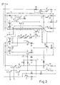
- 1 denotes a differential amplifier, the inverting input 2 and non-inverting input 3 of which form two input connections of an input.
- the differential amplifier 1 outputs a signal to a differential amplifier output 4 which corresponds to the amplified difference between the voltages at the input terminals 2 and 3.
- This is fed to an output 6 via a power amplifier 5 which, in contrast to the differential amplifier 1, has only a low voltage gain, preferably equal to 1, and therefore also functions as an impedance converter stage.
- the inverting input 2 of the differential amplifier 1 corresponding to the first input connection is connected via a feedback resistor 7 to the output 6, which in the present case forms a very simple ohmic feedback network through which a signal from the output 6 is fed back to the input connection 2.
- the gain of the circuit arrangement comprising the differential amplifier 1 and the power amplifier 5 is set in the frequency range of the television signal to be amplified.
- the television signal to be amplified is supplied via two leads 8, 9, to which it is supplied by an arrangement (not shown), for example a demodulator, via an emitter follower stage with a transistor 10, 11 and a current source 12, 13 and an input resistor 14, 15 fed to the input connections 2 and 3, respectively.
- the emitter follower stages 10, 12 and 11, 13 form high-resistance loads for the feeds 8 and 9 and 2 and 3 low-resistance signal sources for the input connections. This has a retroactive effect on the circuit arrangement shown Avoided orders. For this reason, the emitter follower stages 10, 12 and 11, 13 are also not included in the feedback loop formed by the feedback resistor 7.
- an ohmic compensation network formed by a compensation resistor 18 is inserted between the output 6 and the emitter connection of the transistor 11 of the second emitter follower stage 11, 13 in the circuit arrangement according to FIG. 1.
- This compensation resistor 18 is dimensioned such that the signal over it the same influence is exerted on the output 6 on the emitter terminal of the transistor 11 of the second emitter follower stage 11, 13 as on the emitter terminal of the transistor 10 of the first emitter follower stage 10, 12 via the feedback resistor 7 and the input resistor 14. This compensates for the by the first and the second emitter follower stage caused non-linearities.
- the emitter follower stages 10, 12 and 11, 13, the differential amplifier 1 and the power amplifier 5 are supplied with a DC voltage via a common supply voltage connection 19.
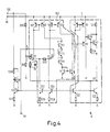
- FIG. 1 The circuit arrangement according to FIG. 1 is executed in more detail in FIG. 3, in particular detailed circuits for the differential amplifier 1 and the power amplifier 5 are specified. For the rest, elements already described in FIG. 1 are again provided with the same reference symbols.
- differential amplifier 1 comprises two emitter-coupled transistors 101, 102, the emitter connections of which are each connected via an emitter resistor 103, 104 to a common current source, consisting of a current source transistor 105 and a current source resistor 106.
- the television signal to be amplified is fed to the base connections of the transistors 101, 102 connected to the input connections 2 and 3. It occurs in an amplified form as a current difference at the collector connections of the transistors 101, 102 and is transmitted to the differential amplifier output 4 by a current mirror arrangement.
- the current mirror arrangement comprises three current mirrors, each with two transistors 107, 108 or 109, 110 or 111, 112.
- a first and a second current mirror transmit them gel 107, 108 or 111, 112 the collector current from the collector connection of transistor 101 and a third current mirror 109, 110 the collector current from the collector connection of transistor 102 in opposite directions to the differential amplifier output 4 such that the current sum is at identical collector currents at transistors 101, 102 in differential amplifier output 4 cancels to zero. Only a push-pull signal thus occurs there, while a common-mode signal is suppressed at the input connections 2, 3 in the differential amplifier 1.
- a chain of three transistors 113, 114, 115 connected as diodes is inserted between the collector connections of transistors 108 and 111 of the first and second current mirrors. These effect a constant potential shift between the transistors 108 and 111 in accordance with the forward voltages of the base-emitter-semiconductor junctions which drop across them. This prevents the transistors 108 and 110 from having too large differences in the collector-emitter voltages, which would lead to signal distortions due to the low "early voltages".
- An internal negative feedback of the differential amplifier 1 is achieved by the emitter resistors 103, 104, which causes a broadband limitation of the no-load gain of the differential amplifier 1 with a minimal phase shift of the signal at the differential amplifier output 4 compared to the signal at the input 2, 3.
- the emitter resistors 103, 104 are dimensioned such that the no-load gain of the differential amplifier 1 falls below 0 dB when the total phase shift between the output 6 and the input 2, 3 of 180 ° (when transitioning to ever higher frequencies of the television signal at the input) and the Circuit arrangement is thus stable.
- the power amplifier 5 which in the present example essentially comprises a Darlington stage composed of two transistors 116, 117, which are controlled by the differential amplifier output 4 via a PNP transistor 118, is connected to the differential amplifier output 4 in the circuit arrangement according to FIG. 3.
- An impressed current from a current source 121 consisting of a transistor and an associated emitter resistor is fed to the PNP transistor 118 via a fourth current mirror consisting of two transistors 119, 120.
- a correspondingly constructed current source 122 feeds the load current path of transistor 117 of the Darlington stage and is connected in series with this and a collector series resistor 123, which serves as a protective resistor in the event of a short circuit at the output, between the supply voltage connection 19 and ground.
- the base-emitter path of transistor 117 is bridged by a parallel resistor 124 as a direct current supply for transistor 116. From the connection point 125 between the transistor 117 and the current source 122, the amplified television signal is fed to the output 6 via an output resistor 126.
- the feedback resistor 7 is also led from the connection point 125 to the first input terminal 2 at the inverting input of the differential amplifier 1.
- the gain of the entire circuit arrangement between the input 2, 3 and the output 6 is set. In essence, this sets the gain in the frequency band of the television signal to be amplified, while the drop in the amplitude-frequency characteristic towards higher frequencies remains essentially unaffected by the feedback resistor 7.
- the television signal to be amplified is fed from the feeds 8, 9 via the two transistors 10, 11 and in their emitter branches as transistors 127, 128 connected as diodes and the input resistors 14, 15 to the input terminals 2 and 3, respectively.
- the transistors 127, 128 are used for shifting the potential between the emitter connections of the transistors 10, 11 and the input connections 2, 3; together with the base-emitter paths of the transistors 10, 11, they each cause a potential jump of two base-emitter forward voltages between the leads 8 and 9 and the input connections 2 and 3, respectively.
- the second input connection 3 is led via the series resistor 16 to the connection 17 of a reference voltage source, at which an essentially constant voltage is present.
- the signal from the connection point 125 is fed to the first input terminal 2 via the feedback resistor 7 with a relatively high amplitude, so that different current levels and thus distortions occur at the transistors 10, 11, 127 and 128.
- the compensation resistor 18 is inserted between the connection point 125 on the one hand and the connection point 129 between the transistor 128 and the current source 13 on the other hand. Part of the signal from the connection point 125 or from the output 6 is also supplied to the transistors 11, 128 via it, so that overall a distortion-free modulation can be achieved.
- the voltage present at the connection 17 is derived from a stabilized voltage supplied via a reference voltage supply connection 130 with the aid of a voltage divider which consists of a series connection of a first resistor 131 with the parallel connection of a second resistor 132 and a series connection of a third resistor 133 with a transistor 134 connected as a diode.
- the transistor 134 forms a shunt with the third resistor 133 to the second resistor 132 carrying the main part of the current flowing in the voltage divider. This shunt is temperature-dependent due to the transistor 134; and the temperature dependency thus generated in the voltage at terminal 17 serves to compensate for the temperature response of the emitter follower stages 10, 11, 127, 128.
- Another voltage divider consisting of a transistor 135, an associated collector and emitter resistor 136 and 137 and a parallel transistor 138, the emitter connection of which is connected to the base connection of transistor 135 and the base connection of which is connected to the collector connection of transistor 135 and the base-collector path in parallel to the collector resistor 136 is connected between the reference voltage supply terminal 130 and ground.
- a control voltage for the current sources 12, 13, 121, 122 and 105, 106 is tapped at the base connection of the transistor 135, the transistors of which each form a current mirror arrangement with the transistor 135.
- the supply voltage connection 19 which is connected to the emitter follower stages 10, 11, 12, 13 and the differential amplifier 1 and the power amplifier 5 for supplying electrical energy, is designed separately from the reference voltage supply connection 130, so that the output 6 may be subjected to high loads in the supply voltage connection 19 interspersed voltage disturbances have no influence on the reference voltages or currents. This also contributes to the low-distortion signal amplification of the circuit arrangement described.
- a voltage which is greater than the reference voltages and from which the latter can be derived is preferably provided at the supply voltage connection 19 for the energy supply.
- the advantage of a separate, preferably separately stabilized voltage at the reference voltage supply connection 130 lies in an improved "hum" suppression (mains hum).
- FIGS. 2 and 4 show a further embodiment of the invention as a block diagram or detailed circuit. Components corresponding to FIGS. 1 and 3 are again provided with identical reference numerals.
- the circuit arrangements according to FIGS. 2 and 4 represent a video post-amplifier which consists of a differential amplifier 100 which is modified compared to the differential amplifier 1 and the power amplifier 5 which is adopted identically.
- This video post-amplifier serves for the post-amplification of the amplified television signal supplied by the video basic amplifier according to FIG. 1 or 3 and is preferably connected to its output 6 via a blocking filter which suppresses the modulated sound signals, a so-called sound carrier trap.
- the arrangement according to FIG. 2 thus represents an embodiment of the invention designed for lower demands on its transmission properties, in particular on its stability.
- the voltage amplification, linearity and stability are the same in the video post-amplifier according to FIGS obtained primarily through the combination of an internal negative feedback and an external feedback.
- the capacitor 70 is preferably dimensioned such that it is only effective in the area of the parasitic higher harmonics for suppressing the same, so that it cannot have a critical influence on the stability.
- it has a capacitance value of the order of 1 pF.
- the first input connection 2 is also connected to the tap of a voltage divider, which is arranged between the reference voltage supply connection 130 and ground, and consists of two resistors 200, 201 for setting the operating point of the differential amplifier 100.
- the differential amplifier 100 largely corresponds to the differential amplifier 1 according to FIG. 3, only the coupling of the emitter connections of the transistors 101, 102 is modified and takes place via a common emitter resistor 202.
- Each of the emitter connections is also provided with an emitter current source consisting of a current source transistor 203 or 204 and one Current source resistor 205 and 206 connected.
- the functioning of this arrangement corresponds essentially to that of the emitter resistors 103, 104 and the common current source 105, 106 according to FIG. 3, but the present configuration is suitable for higher voltage modulations, since there is no additional one between the emitter connections of the transistors 101, 102 and the associated emitter current sources DC voltage drop as occurs at the emitter resistors 103, 104.
- the power amplifier 5 is identical to that from FIG. 3.
- the further voltage divider 135 to 138 for controlling the current source transistors 203, 204 or 121 and 122 also corresponds to FIG. 3.
- the connection point 125 between the Darlington stage 116, 117 and the current source 122 is connected directly to the output 6 in order to obtain a low output resistance.
- a circuit arrangement according to FIG. 3 was dimensioned, for example, for amplifying a television signal by 14 dB to an amplitude of 1 V, an arrangement according to FIG. 4 for further amplifying the television signal by 6 dB to an amplitude of the output voltage of 2 V.
- the values of the components in detail are for this dimensioning example in the following Table listed. With this arrangement, linearity deviations in the amount of the gain of less than 1% and in the phase of less than 1 ° and a distortion factor of less than 1% were achieved.
- the power loss is typically around 13 mW.
Abstract
Description
Die Erfindung bezieht sich auf eine Schaltungsanordnung zum Verstärken eines Fernsehsignals mit einem zwischen einem Eingang und einem Ausgang angeordneten Differenzverstärker mit zwei emittergekoppelten Transistoren.The invention relates to a circuit arrangement for amplifying a television signal with a differential amplifier arranged between an input and an output and having two emitter-coupled transistors.
Derartige Schaltungsanordnungen sind bekannt und werden insbesondere in integrierten Schaltkreisen, beispielsweise zum Verstärken eines Fernsehsignals im Basisband, eingesetzt. Diese integrierten Schaltkreise sind standardmäßig für eine Versorgungsspannung von 12 V ausgelegt und verstärken das Fernsehsignal auf einen Spannungshub von typischer Weise 1 bis 2 V. An solche Anordnungen werden hohe Anforderungen bezüglich des Verstärkungsfaktors, der Linearität und der Stabilität gestellt, ihr Aufbau muß in einem einfach zu handhabenden und damit preiswerten Herstellungsverfahren für integrierte Schaltkreise erfolgen, und die Schaltungsanordnungen müssen selbst auch einen möglichst einfachen und platzsparenden Aufbau haben. Bei den bekannten Schaltungsanordnungen werden diese Anforderungen dadurch erfüllbar, daß der Spannungshub des Fernsehsignals klein gegenüber der Versorgungsspannung bleibt.Such circuit arrangements are known and are used in particular in integrated circuits, for example for amplifying a television signal in the baseband. These integrated circuits are designed for a supply voltage of 12 V as standard and amplify the television signal on a voltage swing of typically 1 to 2 V. Such arrangements have high requirements with regard to the amplification factor, the linearity and the stability, their construction must be simple in one to handle and thus inexpensive manufacturing processes for integrated circuits, and the circuit arrangements themselves must have a simple and space-saving structure. In the known circuit arrangements, these requirements can be met in that the voltage swing of the television signal remains small compared to the supply voltage.
Zur Verringerung der Leistungaufnahme von Fernsehempfängern und dergleichen ist erwünscht, die Versorgungsspannungen für darin enthaltene Schaltungsanordnungen zur Verarbeitung des Fernsehsignals auf einen Wert zu vermindern, der in der Größenordnung des Spannungshubs des Fernsehsignals liegt, insbesondere bei z.B. 5 V. Dadurch wird ein Batteriebetrieb der Fernsehempfänger ermöglicht.In order to reduce the power consumption of television receivers and the like, it is desirable to reduce the supply voltages for circuit arrangements contained therein for processing the television signal to a value which is in the order of magnitude of the voltage swing of the television signal, in particular, for example, 5 V. This enables the television receivers to be operated on batteries .
Andererseits sind für bestimmte Signal-Übertragungseigenschaften bestimmte Ströme erforderlich, die zwecks Leistungsverminderung nicht beliebig verringert werden können. Es zeigt sich, daß die bisher verfolgten Schaltungskonzepte in diesem Fall nicht mehr die an die Verarbeitung des Fernsehsignals zu stellenden Anforderungen insbesondere bezüglich der Linearität und der Stabilität erfüllen.On the other hand, certain currents are required for certain signal transmission properties, which cannot be reduced arbitrarily in order to reduce the power. It turns out that the circuit concepts pursued so far no longer meet the requirements for processing the television signal, in particular with regard to linearity and stability.
Die Erfindung hat die Aufgabe, eine Schaltungsanordnung zum Verstärken eines Fernsehsignals zu schaffen, die mit dem vorgegebenen Herstellungsverfahren erstellt werden kann und dabei trotz niedriger Versorgungsspannung und hoher Aussteuerung durch das Fernsehsignal in hohem Maße linear und stabil arbeitet.The invention has for its object to provide a circuit arrangement for amplifying a television signal, which can be created using the predetermined production method and, despite the low supply voltage and high modulation by the television signal, operates to a high degree in a linear and stable manner.
Die Aufgabe wird bei einer Schaltunsanordnung der eingangs genannten Art erfindungsgemäß durch eine Kombination aus wenigstens einem in die Emitterzweige der Transistoren eingefügten ohmschen Widerstand und einem ohmschen Rückkopplungsnetzwerk zum Rückführen eines Signals vom Ausgang zum Eingang gelöst.The object is achieved according to the invention in a circuit arrangement of the type mentioned at the outset by a combination of at least one ohmic resistor inserted into the emitter branches of the transistors and an ohmic feedback network for feeding back a signal from the output to the input.
Das eingangs genannte, bevorzugt zu verwendende Herstellungs-(Diffusions-)Verfahren zur Herstellung von integrierten Schaltkreisen auf einem Halbleiterplättchen zeichnet sich dadurch aus, daß bei der Diffusion Bauelemente mit geringen Schichtdicken entstehen. Es wird gewählt, um Bauelemente und Schaltungen mit guten Hochfrequenzeigenschaften zu erhaltn, die insbesondere für die ZF-Signalverarbeitung in Fernseh-Empfangsanordnungen benötigt werden. Es zeigt sich, daß die damit erzeugten (bipolaren) Transistoren eine verhältnismäßig geringe "Early-Spannung" entsprechend einer verhältnismäßig hohen Abhängigkeit der Kollektorströme dieser Transistoren von ihren Kollektor-Emitter-Spannungen auch im Verstärkerbereich aufweisen. Dadurch werden insbesondere bei höheren Strom-bzw. Spannungshüben an den Transistoren nichtlineare Verzerrungen hervorgerufen, die sich besonders stark bei niedrigen Versorgungsspannungen und zugleich hohen Signal-Spannungshüben bemerkbar machen. Durch die Maßnahmen nach der Erfindung wird der Einfluß dieser Nichtlinearitäten auf die Verstärkungscharakteristik soweit vermindert, daß die hohen Anforderungen an die Linearität bei der Verarbeitung des Fernsehsignals erfüllt werden können. Insbesondere wird dadurch eine Schaltungsanordnung zum Verstärken eines Fernsehsignals geschaffen, die über das gesamte vom Fernsehsignal beanspruchte Frequenzband eine gleichmäßig hohe Verstärkung sowie oberhalb dieses Frequenzbandes einen steilen Abfall der Amplituden-Frequenz-Charakteristik aufweist. Eine hohe Verstärkung des Nutzsignals wird so mit einer hohen Stabilität der über das ohmsche Rückkopplungsnetzwerk rückgekoppelten Schaltungsanordnung verbunden. Durch Verwenden eines rein ohmschen Rückkopplungsnetzwerks wird dabei eine geringe Phasendrehung zwischen dem Fernsehsignal am Eingang und dem Signal am Ausgang und damit eine hohe Stabilität erzielt.The above-mentioned, preferably used manufacturing (diffusion) method for manufacturing integrated circuits on a semiconductor wafer is characterized in that components with small layer thicknesses are formed during diffusion. It is chosen in order to obtain components and circuits with good high-frequency properties, which are required in particular for IF signal processing in television reception arrangements. It turns out that the (bipolar) transistors produced thereby have a relatively low "early voltage" corresponding to a relatively high dependence of the collector currents of these transistors on them Also have collector-emitter voltages in the amplifier area. As a result, especially at higher current or. Voltage swings on the transistors caused nonlinear distortions, which are particularly noticeable at low supply voltages and at the same time high signal voltage swings. The measures according to the invention reduce the influence of these non-linearities on the amplification characteristic to such an extent that the high linearity requirements can be met when processing the television signal. In particular, this creates a circuit arrangement for amplifying a television signal which has a uniformly high amplification over the entire frequency band claimed by the television signal and a steep drop in the amplitude-frequency characteristic above this frequency band. A high amplification of the useful signal is thus associated with a high stability of the circuit arrangement fed back via the ohmic feedback network. By using a purely ohmic feedback network, a small phase shift between the television signal at the input and the signal at the output and thus a high degree of stability are achieved.
Die Kombination des ohmschen Widerstands in den Emitterzweigen mit dem ohmschen Rückkopplungsnetzwerk ermöglicht vorteilhaft eine Einstellung der Amplituden-Frequenz-Charakteristik der Schaltungsanordnung in ihren beiden Freiheitsgraden. Durch die Emitterwiderstände wird im wesentlichen der Abfall der Amplituden-Frequenz-Charakteristik oberhalb des Frequenzbandes des Fernsehsignals und damit die Stabilität bestimmt, wohingegen das ohmsche Rückkopplungsnetzwerk im wesentlichen die Einstellung der Verstärkung innerhalb des Frequenzbandes des Fernsehsignals bedingt. Die erfindungsgemäße Schaltungsanordnung weist eine sehr hohe Linerarität auf, die sich in einer sehr geringen Amplituden- und Phasenverzerrung und somit einem sehr niedrigen Klirrfaktor bemerkbar macht. Damit sind bei niedriger Versorgungsspannung und dadurch bedingter niedriger Verlustleistung hohe Spannungshübe des Fernsehsignals am Ausgang erzielbar. Die Verstärkung im Frequenzband des Fernsehsignals ist in weiten Bereichen allein durch die Dimensionierung des ohmschen Rückkopplungsnetzwerks bei gleichbleibend guter Linerarität frei wählbar. Die erfindungsgemäße Schaltungsanordnung weist dabei ein hohes Verstärkungs-Bandbreite-Produkt bei gleichzeitig guter Stabilität auf. Durch Verwenden eines frequenzunabhängigen Rückkopplungsnetzwerks sowie Widerstands in den Emitterzweigen ist darüber hinaus ein sehr gleichmäßiger Verlauf der Amplituden-Frequenz-Charakteristik im Frequenzband des Fernsehsignals gewährleistet.The combination of the ohmic resistance in the emitter branches with the ohmic feedback network advantageously makes it possible to set the amplitude-frequency characteristic of the circuit arrangement in its two degrees of freedom. The drop in the amplitude-frequency characteristic above the frequency band of the television signal and thus the stability is essentially determined by the emitter resistances, whereas the ohmic feedback network essentially requires the adjustment of the gain within the frequency band of the television signal. The circuit arrangement according to the invention has a very high linearity, which is reflected in a very low amplitude and phase distortion and thus a very low distortion factor. High voltage swings of the television signal at the output can thus be achieved with a low supply voltage and the resulting low power loss. The gain in the frequency band of the television signal can be freely selected in a wide range solely through the dimensioning of the ohmic feedback network with consistently good linearity. The circuit arrangement according to the invention has a high gain-bandwidth product with good stability at the same time. By using a frequency-independent feedback network and resistance in the emitter branches, a very even course of the amplitude-frequency characteristic in the frequency band of the television signal is also guaranteed.
Vorteilhaft wird das Fernsehsignal dem Eingang über wenigstens eine Emitterfolgerstufe zugeleitet. Dadurch wird eine Impedanzwandlung und Entkopplung von voraufgehenden, das Fernsehsignal liefernden Schaltungsteilen erreicht. Das ist insbesondere dann von Vorteil, wenn die erfindungsgemäße Schaltungsanordnung unmittelbar vom Ausgang eines Demodulators gespeist wird. Die Emitterfolgerstufen verhindern dann eine Rückwirkung auf den Demodulator und unterdrücken anderenfalls im Demodulator hervorgerufene Signalverzerrungen.The television signal is advantageously fed to the input via at least one emitter follower stage. This achieves an impedance conversion and decoupling of preceding circuit parts which supply the television signal. This is particularly advantageous if the circuit arrangement according to the invention is fed directly from the output of a demodulator. The emitter follower stages then prevent feedback on the demodulator and otherwise suppress signal distortions caused in the demodulator.
In einer vorteilhaften Weiterbildung enthält eine erfindungsgemäße Schaltungsanordnung mit einem Eingang mit zwei Eingangsanschlüssen, von denen ein erster mit dem Rückkopplungsnetzwerk verbunden ist, ein ohmsches Kompensationsnetzwerk zum Einspeisen eines Anteils des Signals vom Ausgang auf einen zweiten der Eingangsanschlüsse. Wenn von zwei Eingangsanschlüssen nur einer zwecks Rückkopplung mit dem Signal vom Ausgang beaufschlagt wird, liegen an ihnen unterschiedliche Spannungen, durch die die Schaltungsanordnung unterschiedlich ausgesteuert wird. Insbesondere werden dadurch mit den Eingangsanschlüssen verbundene Emitterfolgerstufen unterschiedlich ausgesteuert, so daß an ihnen nichtlineare Verzerrungen auftreten. Durch das ohmsche Kompensationsnetzwerk wird ein Anteil des Signals vom Ausgang der Schaltungsanordnung auch dem zweiten Eingangsanschluß und damit der zweiten mit ihm gekoppelten Emitterfolgerstufe zugeführt derart, daß die Emitterfolgerstufen gleichmäßig ausgesteuert werden. Ihre Aussteuerungsbereiche in den Kennlinienfeldern der sie bildenden Transistoren sind dann identisch, so daß übereinstimmende Strom- und Spannungsverläufe im gesamten durch das Fernsehsignal bedingten Aussteuerbereich erzielt werden können.In an advantageous development, a circuit arrangement according to the invention with an input with two input connections, a first of which is connected to the feedback network, contains an ohmic compensation network for feeding a portion of the signal from the output to a second of the input connections. If of two input connections only one for feedback with When the signal is acted upon by the output, there are different voltages at them, by means of which the circuit arrangement is controlled differently. In particular, this means that emitter follower stages connected to the input connections are driven differently, so that nonlinear distortions occur at them. Through the ohmic compensation network, a portion of the signal from the output of the circuit arrangement is also fed to the second input terminal and thus to the second emitter follower stage coupled to it in such a way that the emitter follower stages are driven uniformly. Their modulation ranges in the characteristic fields of the transistors forming them are then identical, so that matching current and voltage profiles can be achieved in the entire modulation range caused by the television signal.
Einige Ausführungsbeispiele der Erfindung sind in der Zeichnung dargestellt und werden im nachfolgenden näher beschrieben. Es zeigen:
- Fig. 1 ein Blockschaltbild eines ersten Beispiels einer erfindungsgemäßen Schaltungsanordnung, die als Video-Grundverstärker ausgeführt ist,
- Fig. 2 ein Blockschaltbild eines weiteren Ausführungsbeispiels der Erfindung, das als Video-Nachverstärker ausgelegt ist,
- Fig. 3 ein detailliertes Schaltbild des Ausführungsbeispiels nach Fig. 1,
- Fig. 4 ein detailliertes Schaltbild des Ausführungsbeispiels nach Fig. 2.
- 1 is a block diagram of a first example of a circuit arrangement according to the invention, which is designed as a video basic amplifier,
- 2 shows a block diagram of a further exemplary embodiment of the invention, which is designed as a video post-amplifier,
- 3 is a detailed circuit diagram of the embodiment of FIG. 1,
- FIG. 4 shows a detailed circuit diagram of the exemplary embodiment according to FIG. 2.
Im Blockschaltbild nach Fig. 1 ist mit 1 ein Differenzverstärker bezeichnet, dessen invertierender Eingang 2 und nichtinvertierender Eingang 3 zwei Eingangsanschlüsse eines Eingangs bilden. Der Differenzverstärker 1 gibt an einen Differenzverstärkerausgang 4 ein Signal ab, das der verstärkten Differenz der Spannungen an den Eingangsanschlüssen 2 und 3 entspricht. Dieses wird über einen Leistungsverstärker 5, der im Gegensatz zum Differenzverstärker 1 nur eine niedrige Spannungsverstärkung, vorzugsweise gleich 1, aufweist, und daher auch als Impedanzwandlerstufe fungiert, einem Ausgang 6 zugeleitet.In the block diagram according to FIG. 1, 1 denotes a differential amplifier, the inverting
Der invertierende Eingang 2 des Differenzverstärkers 1 entsprechend dem ersten Eingangsanschluß ist über einen Rückkopplungswiderstand 7 mit dem Ausgang 6 verbunden, der ein im vorliegenden Fall sehr einfaches ohmsches Rückkopplungsnetzwerk bildet, durch das ein Signal vom Ausgang 6 zum Eingangsanschluß 2 zurückgeführt wird. Durch diese Rückkopplung wird die Verstärkung der den Differenzverstärker 1 und den Leistungsverstärker 5 umfassenden Schaltungsanordnung im Frequenzbereich des zu verstärkenden Fernsehsignals eingestellt.The inverting
Das zu verstärkende Fernsehsignal wird über zwei Zuführungen 8, 9, an die es von einer nicht dargestellten Anordnung, beispielsweise einem Demodulator, geliefert wird, über je eine Emitterfolgerstufe mit je einem Transistor 10, 11 und je einer Stromquelle 12, 13 sowie je einen Eingangswiderstand 14, 15 den Eingangsanschlüssen 2 bzw. 3 zugeleitet. Die Emitterfolgerstufen 10, 12 bzw. 11, 13 bilden für die Zuführungen 8 bzw. 9 hochohmige Belastungen und für die Eingangsanschlüsse 2 bzw. 3 niederohmige Signalquellen. Dadurch wird eine Rückwirkung auf der dargestellten Schaltungsanordnung vorgeschaltete Anordnungen vermieden. Die Emitterfolgerstufen 10, 12 und 11, 13 sind aus diesem Grunde auch nicht in die durch den Rückkopplungswiderstand 7 gebildete Rückkopplungsschleife einbezogen. Daher werden Nichtlinearitäten im Übertragungsverhalten der dargestellten Schaltungsanordnung, die durch die Transistoren 10, 11 der Emitterfolgerstufen hervorgerufen werden können, durch die Rückkopplungsschleife nicht ausgeglichen. Dafür dienen vielmehr zum einen die Stromquellen 12 bzw. 13, durch die den Transistoren 10 bzw. 11 feste Ströme eingeprägt werden, sowie eine geringe Aussteuerung der Transistoren 10, 11 an ihren Basisanschlüssen, wodurch verhindert wird, daß die Eingangskennlinien der Transistoren 10 bzw. 11 in merkbar nichtlineare Bereiche ausgesteuert werden.The television signal to be amplified is supplied via two
Zum anderen entsteht jedoch eine nichtlineare Verzerrung der Spannungen an den Eingangsanschlüssen 2 und 3 durch die unterschiedliche, vom zu verstärkenden Fernsehsignal abhängige Belastung des ersten Eingangsanschlusses 2 durch das Signal am Ausgang 6 über den Rückkopplungswiderstand 7. Dadurch wird der Emitteranschluß des Transistors 10 der ersten Emitterfolgerstufe mit einem signalabhängigen Strom beaufschlagt, der über die Strom-Spannungs-Charakteristik des Transistors 10 am ersten Eingangsanschluß 2 eine Spannungsverzerrung hervorruft. Diese tritt am zweiten Eingangsanschluß 3, der über einen Vorwiderstand 16 mit dem Anschluß 17 einer Referenzspannungsquelle verbunden ist, die eine konstante Gleichspannung abgibt, nicht auf. Zum Unterdrücken derartiger Nichtlinearitäten ist in der Schaltungsanordnung nach Fig. 1 ein durch einen Kompensationswiderstand 18 gebildetes ohmsches Kompensationsnetzwerk zwischen dem Ausgang 6 und dem Emitteranschluß des Transistors 11 der zweiten Emitterfolgerstufe 11, 13 eingefügt. Dieser Kompensationswiderstand 18 ist derart bemessen, daß über ihn vom Signal am Ausgang 6 auf den Emitteranschluß des Transistors 11 der zweiten Emitterfolgerstufe 11, 13 der gleiche Einfluß ausgeübt wird wie auf den Emitteranschluß des Transistors 10 der ersten Emitterfolgerstufe 10, 12 über den Rückkopplungswiderstand 7 und den Eingangswiderstand 14. Damit kompensieren sich die durch die erste und die zweite Emitterfolgerstufe verursachten Nichtlinearitäten.On the other hand, however, there is a non-linear distortion of the voltages at the
Die Emitterfolgerstufen 10, 12 bzw. 11, 13, der Differenzverstärker 1 und der Leistungsverstärker 5 werden über einen gemeinsamen Versorgungsspannungsanschluß 19 mit einer Gleichspannung versorgt.The
In Fig. 3 ist die Schaltungsanordnung nach Fig. 1 detaillierter ausgeführt, insbesondere sind Detailschaltungen für den Differenzverstärker 1 und den Leistungsverstärker 5 angegeben. Im übrigen sind in Fig. 1 bereits beschriebene Elemente wieder mit denselben Bezugszeichen versehen.The circuit arrangement according to FIG. 1 is executed in more detail in FIG. 3, in particular detailed circuits for the differential amplifier 1 and the
Der Differenzverstärker 1 umfaßt gemäß Fig. 3 zwei emittergekoppelte Transistoren 101, 102, deren Emitteranschlüsse über je einen Emitterwiderstand 103, 104 mit einer gemeinsamen Stromquelle, bestehend aus einem Stromquellentransistor 105 und einem Stromquellenwiderstand 106, verbunden sind. Über die mit den Eingangsanschlüssen 2 und 3 verbundenen Basisanschlüsse der Transistoren 101, 102 wird diesen das zu verstärkende Fernsehsignal zugeführt. Es tritt in verstärkter Form als Stromdifferenz an den Kollektoranschlüssen der Transistoren 101, 102 auf und wird durch eine Stromspiegelanordnung an den Differenzverstärkerausgang 4 übertragen.According to FIG. 3, differential amplifier 1 comprises two emitter-coupled
Die Stromspiegelanordnung umfaßt drei Stromspiegel mit je zwei Transistoren 107, 108 bzw. 109, 110 bzw. 111, 112. Dabei übertragen ein erster und ein zweiter Stromspie gel 107, 108 bzw. 111, 112 den Kollektorstrom vom Kollektoranschluß des Transistors 101 und ein dritter Stromspiegel 109, 110 den Kollektorstrom vom Kollektoranschluß des Transistors 102 gegensinnig auf den Differenzverstärkerausgang 4 derart, daß sich bei identischen Kollektorströmen an den Transistoren 101, 102 die Stromsumme im Differenzverstärkerausgang 4 gerade zu Null aufhebt. Dort tritt somit nur ein Gegentaktsignal auf, während ein Gleichtaktsignal an den Eingangsanschlüssen 2, 3 im Differenzverstärker 1 unterdrückt wird.The current mirror arrangement comprises three current mirrors, each with two
Zwischen die Kollektoranschlüsse der Transistoren 108 und 111 des ersten und zweiten Stromspiegels ist eine Kette von drei als Dioden geschalteten Transistoren 113, 114, 115 eingefügt. Diese bewirken zwischen den Transistoren 108 und 111 eine konstante Potentialverschiebung entsprechend der an ihnen abfallenden Durchlaßspannungen der Basis-Emitter-Halbleiterübergänge. Dadurch wird vermieden, daß an den Transistoren 108 und 110 zu große Unterschiede der Kollektor-Emitter-Spannungen auftreten, die aufgrund der geringen "Early-Spannungen" zu Signalverzerrungen führen würden.A chain of three
Durch die Emitterwiderstände 103, 104 wird eine interne Gegenkopplung des Differenzverstärkers 1 erzielt, die eine breitbandige Begrenzung der Leerlaufverstärkung des Differenzverstärkers 1 mit minimaler Phasendrehung des Signals am Differenzverstärkerausgang 4 gegenüber dem Signal am Eingang 2, 3 bewirkt. Die Emitterwiderstände 103, 104 werden so dimensioniert, daß die Leerlaufverstärkung des Differenzverstärkers 1 bei Erreichen einer Gesamtphasendrehung zwischen dem Ausgang 6 und dem Eingang 2, 3 von 180° (beim Übergang zu immer höheren Frequenzen des Fernsehsignals am Eingang) unter 0 dB gefallen und die Schaltungsanordnung damit stabil ist.An internal negative feedback of the differential amplifier 1 is achieved by the
An den Differenzverstärkerausgang 4 schließt sich in der Schaltungsanordnung nach Fig. 3 der Leistungsverstärker 5 an, der im vorliegenden Beispiel im wesentlichen eine Darlington-Stufe aus zwei Transistoren 116, 117 umfaßt, die über einen PNP-Transistor 118 vom Differenzverstärkerausgang 4 angesteuert werden. Dem PNP-Transistor 118 wird über einen vierten Stromspiegel aus zwei Transistoren 119, 120 ein eingeprägter Strom von einer aus einem Transistor und einem zugehörigen Emitterwiderstand bestehenden Stromquelle 121 zugeführt. Eine entsprechend aufgebaute Stromquelle 122 speist den Laststrompfad des Transistors 117 der Darlington-Stufe und ist dazu mit diesem und einem Kollektor-Vorwiderstand 123,der als Schutzwiderstand für den Fall eines Kurzschlusses am Ausgang dient, zwischen dem Versorungsspannungsanschluß 19 und Masse in Reihe geschaltet. Außerdem ist die Basis-Emitter-Strecke des Transistors 117 durch einen Parallelwiderstand 124 als Gleichstromspeisung für den Transistor 116 überbrückt. Vom Verbindungspunkt 125 zwischen dem Transistor 117 und der Stromquelle 122 wird das verstärkte Fernsehsignal über einen Ausgangswiderstand 126 dem Ausgang 6 zugeleitet.The
Vom Verbindungspunkt 125 ist außerdem der Rückkopplungswiderstand 7 an den ersten Eingangsanschluß 2 am invertierenden Eingang des Differenzverstärkers 1 geführt. Durch Wahl der Größe des Rückkopplungswiderstands 7 wird die Verstärkung der gesamten Schaltungsanordnung zwischen dem Eingang 2, 3 und dem Ausgang 6 eingestellt. Im wesentlichen wird dadurch die Verstärkung im Frequenzband des zu verstärkenden Fernsehsignals eingestellt, während der Abfall der AmplitudenFrequenz-Charakteristik zu höheren Frequenzen hin durch den Rückkopplungswiderstand 7 im wesentlichen unbeeinflußt bleibt.The feedback resistor 7 is also led from the
Das zu verstärkende Fernsehsignal wird von den Zuführungen 8, 9 über die beiden Transistoren 10, 11 sowie in deren Emitterzweige als Dioden geschaltete Transistoren 127, 128 und die Eingangswiderstände 14, 15 den Eingangsanschlüssen 2 bzw. 3 zugeleitet. Die Transistoren 10, 11, 127, 128 bilden zusammen mit den Stromquellen 12, 13, die ebenfalls aus je einem Transistor mit Emitterwiderstand bestehen, zwei Emitterfolgerstufen zum rückwirkungsarmen Zuführen des zu verstärkenden Fernsehsignals an den Differenzverstärker 1. Die Transistoren 127, 128 dienen zur Potentialverschiebung zwischen den Emitteranschlüssen der Transistoren 10, 11 und den Eingangsanschlüssen 2, 3; zusammen mit den Basis-Emitter-Strecken der Transistoren 10, 11 rufen sie je einen Potentialsprung von zwei Basis-Emitter-Flußspannungen zwischen den Zuführungen 8 bzw. 9 und den Eingangsanschlüssen 2 bzw. 3 hervor.The television signal to be amplified is fed from the
Der zweite Eingangsanschluß 3 ist über den Vorwiderstand 16 an den Anschluß 17 einer Referenzspannungsquelle geführt, an dem eine im wesentlichen konstante Spannung anliegt. Dagegen wird dem ersten Eingangsanschluß 2 über den Rückkopplungswiderstand 7 das Signal vom Verbindungspunkt 125 mit relativ hoher Amplitude zugeführt, so daß an den Transistoren 10, 11, 127 und 128 unterschiedliche Stromaussteuerungen und damit Verzerrungen auftreten. Um diese auszuschließen, ist zwischen dem Verbindungspunkt 125 einerseits und dem Verbindungspunkt 129 zwischen dem Transistor 128 und der Stromquelle 13 andererseits der Kompensationswiderstand 18 eingefügt. Über ihn wird ein Teil des Signals vom Verbindungspunkt 125 bzw. vom Ausgang 6 auch den Transitoren 11, 128 zugeführt, so daß insgesamt eine verzerrungsfreie Aussteuerung erreicht werden kann.The
Die am Anschluß 17 anliegende Spannung wird aus einer über einen Referenzspannungs-Speiseanschluß 130 zugeführten, stabilisierten Spannung mit Hilfe eines Spannungsteilers abgeleitet, der aus einer Reihenschaltung eines ersten Widerstands 131 mit der Parallelschaltung aus einem zweiten Widerstand 132 und einer Reihenschaltung eines dritten Widerstands 133 mit einem als Diode geschalteten Transistor 134 besteht. Der Transistor 134 bildet mit dem dritten Widerstand 133 einen Nebenschluß zu dem den Hauptanteil des im Spannungsteiler fließenden Stromes führenden zweiten Widerstand 132. Dieser Nebenschluß ist durch den Transistor 134 temperaturabhängig; und die so in der Spannung am Anschluß 17 erzeugte Temperaturabhängigkeit dient zur Kompensation des Temperaturgangs der Emitterfolgerstufen 10, 11, 127, 128.The voltage present at the
Ein weiterer Spannungsteiler aus einem Transistor 135, einem zugehörigen Kollektor- und Emitterwiderstand 136 bzw. 137 sowie einem Paralleltransistor 138, dessen Emitteranschluß mit dem Basisanschluß des Transistors 135 und dessen Basisanschluß mit dem Kollektoranschluß des Transistors 135 verbunden ist und dessen Basis-Kollektor-Strecke parallel zum Kollektorwiderstand 136 liegt, ist zwischen den Referenzspannungs-Speiseanschluß 130 und Masse geschaltet. Am Basisanschluß des Transistors 135 wird eine Steuerspannung für die Stromquellen 12, 13, 121, 122 bzw. 105, 106 abgegriffen, deren Transistoren mit dem Transistor 135 je eine Stromspiegelanordnung bilden.Another voltage divider consisting of a
Der mit den Emitterfolgerstufen 10, 11, 12, 13 sowie dem Differenzverstärker 1 und dem Leistungsverstärker 5 zum Zuführen elektrischer Energie verbundene Versorgungsspannungsanschluß 19 ist vom Referenzspannungs-Speiseanschluß 130 getrennt ausgeführt, so daß gegebenenfalls durch hohe Belastung des Ausgangs 6 in den Versorgungs spannungsanschluß 19 eingestreute Spannungsstörungen keinen Einfluß auf die Referenzspannungen bzw. -ströme haben. Auch dies trägt zur verzerrungsarmen Signalverstärkung der beschriebenen Schaltungsanordnung bei. Außerdm wird am Versorgungsspannungsanschluß 19 zur Energieversorgung vorzugsweise eine Spannung bereitgestellt, die größer als die Referenzspannungen ist und aus der die letzteren abgeleitet werden können. Der Vorteil einer getrennten, vorzugsweise gesondert stabilisierten Spannung am Referenzspannungs-Speiseanschluß 130 liegt in einer verbesserten "Brumm"-Unterdrückung (Netzbrummen).The
Fig. 2 und 4 zeigen ein weiteres Ausführungsbeispiel der Erfindung als Blockschaltbild bzw. detaillierte Schaltung. Mit Fig. 1 und 3 übereinstimmende Bestandteile sind wieder mit identischen Bezugszeichen versehen. Die Schaltungsanordnungen nach Fig. 2 und 4 stellen einen Video-Nachverstärker dar, der aus einem gegenüber dem Differenzverstärker 1 abgewandelten Differenzverstärker 100 sowie dem identisch übernommenen Leistungsverstärker 5 besteht. Dieser Video-Nachverstärker dient zur Nachverstärkung des vom Video-Grundverstärker nach Fig. 1 oder 3 gelieferten, verstärkten Fernsehsignals und wird an dessen Ausgang 6 bevorzugt über ein die modulierten Tonsignale unterdrükkendes Sperrfilter, eine sogenannte Tonträgerfalle, angeschlossen. Der Video-Nachverstärker nach Fig. 2 und 4 enthält dafür im Gegensatz zum Video-Grundverstärker einen Eintakt-Eingang 90, der unmittelbar an den zweiten Eingangsanschluß 3 angeschlossen ist, der durch den nichtinvertierenden Eingang des Differenzverstärkers 100 gebildet wird, und die Emitterfolgerstufen der Fig. 1 und 3 und alle damit in Zusammenhang stehenden Schaltungsteile entfallen beim Video-Nachverstärker. Dieser dient der Leistungsverstärkung, weist jedoch einen relativ geringen Spannungsverstärkungsfaktor auf. Die Anforderun gen zur Erreichung von Linearität und Stabilität sind niedriger als bei den Anordnungen nach den Fig. 1 und 3. Parallel zum Rückkopplungswiderstand 7 kann daher ein Kondensator 70 geschaltet sein, der eine tiefpaßartige Rückkopplung mit im Vergleich zu den Anordnungen nach Fig. 1 und 3 stärkerer Phasendrehung bewirkt. Mit dieser Anordnung wird eine höhere Spannungsverstärkung bei gleichzeitiger Stabilität nicht mehr erreicht.2 and 4 show a further embodiment of the invention as a block diagram or detailed circuit. Components corresponding to FIGS. 1 and 3 are again provided with identical reference numerals. The circuit arrangements according to FIGS. 2 and 4 represent a video post-amplifier which consists of a
Die Anordnung nach Fig. 2 stellt damit eine auf geringere Anforderungen an ihre Übertragungseigenschaften, insbesondere an ihre Stabilität, ausgelegte Ausführungsform der Erfindung dar. Wie auch im Video-Grundverstärker wird beim Video-Nachverstärker nach Fig. 2 und 4 die Spannungsverstärkung, Linearität und Stabilität in erster Linie durch die Kombination einer internen Gegenkopplung und einer externen Rückkopplung erhalten. Der Kondensator 70 ist bevorzugt derart dimensioniert, daß er erst im Bereich der parasitären höheren Harmonischen zum Unterdrücken derselben wirksam wird, so daß er keinen kritischen Einfluß auf die Stabilität ausüben kann. Er weist insbesondere einen Kapazitätswert in der Größenordnung von 1 pF auf. Beim vorliegenden Herstellungsverfahren bedeutet dies eine Kondensatorfläche auf dem Halbleiterplättchen von ungefähr einem Tausendstel Quadratmillimeter. Die bei der Herstellung derartiger Flächen auftretenden Fertigungstoleranzen könnten zu Instabilitäten führen, wenn der Kondensator 70 einen entscheidenden Einfluß auf die Stabilität der Schaltungsanordnung hätte.The arrangement according to FIG. 2 thus represents an embodiment of the invention designed for lower demands on its transmission properties, in particular on its stability. As in the video basic amplifier, the voltage amplification, linearity and stability are the same in the video post-amplifier according to FIGS obtained primarily through the combination of an internal negative feedback and an external feedback. The
Im Video-Nachverstärker nach Fig. 2 ist der erste Eingangsanschluß 2 weiterhin mit dem Abgriff eines zwischen dem Referenzspannungs-Speiseanschluß 130 und Masse angeordneten Spannungsteilers aus zwei Widerständen 200, 201 verbunden zum Einstellen des Arbeitspunktes des Differenzverstärkers 100.In the video post-amplifier according to FIG. 2, the
Im detaillierten Schaltbild nach Fig. 4 sind die Bauteile des Differenzverstärkers 100 durch eine gestrichelte Linie umrandet. Der Differenzverstärker 100 entspricht weitgehend dem Differenzverstärker 1 nach Fig. 3, lediglich die Kopplung der Emitteranschlüsse der Transistoren 101, 102 ist abgewandelt und erfolgt über einen gemeinsamen Emitterwiderstand 202. Jeder der Emitteranschlüsse ist außerdem mit einer Emitterstromquelle aus einem Stromquellentransistor 203 bzw. 204 und einem Stromquellenwiderstand 205 bzw. 206 verbunden. Die Funktionsweise dieser Anordnung entspricht im wesentlichen derjenigen der Emitterwiderstände 103, 104 und der gemeinsamen Stromquelle 105, 106 nach Fig. 3, die vorliegende Konfiguration ist jedoch für höhere Spannungsaussteuerungen geeignet, da zwischen den Emitteranschlüssen der Transistoren 101, 102 und den zugehörigen Emitterstromquellen kein zusätzlicher Gleichstrom-Spannungsabfall wie an den Emitterwiderständen 103, 104 auftritt.In the detailed circuit diagram according to FIG. 4, the components of the
Der Leistungsverstärker 5 ist mit demjenigen aus Fig. 3 identisch. Auch der weitere Spannungsteiler 135 bis 138 zur Steuerung der Stromquellentransistoren 203, 204 bzw. von 121 und 122 stimmt mit Fig. 3 überein. Dagegen ist der Verbindungspunkt 125 zwischen der Darlington-Stufe 116, 117 und der Stromquelle 122 unmittelbar mit dem Ausgang 6 verbunden, um einen niedrigen Ausgangswiderstand zu erhalten.The
Eine Schaltungsanordnung gemäß Fig. 3 wurde beispielsweise für eine Verstärkung eines Fernsehsignals um 14 dB auf eine Amplitude von 1 V, eine Anordnung nach Fig. 4 für eine weitere Verstärkung des Fernsehsignals um 6 dB auf eine Amplitude der Ausgangsspannung von 2 V dimensioniert. Die Werte der Bauelemente im einzelnen sind für dieses Dimensionierungsbeispiel in der nachfolgenden Tabelle aufgeführt. Mit dieser Anordnung wurden Linearitätsabweichungen im Betrag der Verstärkung von weniger als 1 % und in der Phase von weniger als 1 ° sowie ein Klirrfaktor von weniger als 1 % erreicht. Die Verlustleistung beträgt typischer Weise etwa 13 mW.


Claims (3)
gekennzeichnet durch eine Kombination aus wenigstens einem in die Emitterzweige der Transistoren eingefügten ohmschen Widerstand (103, 104; 202) und einem ohmschen Rückkopplungsnetzwerk (7) zum Rückführen eines Signals vom Ausgang (6) zum Eingang (2, 3).1. Circuit arrangement for amplifying a television signal with a differential amplifier with two emitter-coupled transistors arranged between an input and an output,
characterized by a combination of at least one ohmic resistor (103, 104; 202) inserted into the emitter branches of the transistors and an ohmic feedback network (7) for feeding back a signal from the output (6) to the input (2, 3).
gekennzeichnet durch wenigstens eine Emitterfolgerstufe (10, 127, 12 bzw. 11, 128, 13), über die das Fernsehsignal dem Eingang (2, 3) zugeleitet wird.2. Circuit arrangement according to claim 1,
characterized by at least one emitter follower stage (10, 127, 12 or 11, 128, 13), via which the television signal is fed to the input (2, 3).
gekennzeichnet durch ein ohmsches Kompensationsnetzwerk (18) zum Einspeisen eines Anteils des Signals vom Ausgang (6) auf einen zweiten der Eingangsanschlüsse (2).3. Circuit arrangement according to claim 2 with an input having two input connections, a first of which is connected to the feedback network,
characterized by an ohmic compensation network (18) for feeding a portion of the signal from the output (6) to a second one of the input connections (2).
Applications Claiming Priority (2)
| Application Number | Priority Date | Filing Date | Title |
|---|---|---|---|
| DE19873714643 DE3714643A1 (en) | 1987-05-02 | 1987-05-02 | CIRCUIT ARRANGEMENT FOR AMPLIFYING A TELEVISION SIGNAL |
| DE3714643 | 1987-05-02 |
Publications (3)
| Publication Number | Publication Date |
|---|---|
| EP0290080A2 true EP0290080A2 (en) | 1988-11-09 |
| EP0290080A3 EP0290080A3 (en) | 1990-12-12 |
| EP0290080B1 EP0290080B1 (en) | 1996-07-10 |
Family
ID=6326693
Family Applications (1)
| Application Number | Title | Priority Date | Filing Date |
|---|---|---|---|
| EP88200795A Expired - Lifetime EP0290080B1 (en) | 1987-05-02 | 1988-04-26 | Television signal amplifying circuitry |
Country Status (4)
| Country | Link |
|---|---|
| US (1) | US4994756A (en) |
| EP (1) | EP0290080B1 (en) |
| JP (1) | JP3022564B2 (en) |
| DE (2) | DE3714643A1 (en) |
Families Citing this family (10)
| Publication number | Priority date | Publication date | Assignee | Title |
|---|---|---|---|---|
| US5093728A (en) * | 1990-08-02 | 1992-03-03 | Thomson Consumer Electronics, Inc. | Beam scan velocity modulation apparatus |
| US5196941A (en) * | 1990-08-02 | 1993-03-23 | Rca Licensing Corporation | Beam scan velocity modulation apparatus |
| CA2072436C (en) * | 1991-06-28 | 2001-01-30 | Fumiaki Honda | Capacitive circuit |
| DE4222033C2 (en) * | 1992-07-04 | 1994-09-01 | Zdf | Video output stage |
| US5864254A (en) * | 1995-04-11 | 1999-01-26 | Rohm Co., Ltd. | Differential amplifier circuit with enlarged range for source voltage and semiconductor device using same |
| US5661436A (en) * | 1996-04-19 | 1997-08-26 | Eastman Kodak Company | High bandwidth video output amplifier circuit for high resolution cathode ray tube image displays |
| US7239198B1 (en) * | 1998-12-14 | 2007-07-03 | Ati International Srl | Single gate oxide differential receiver and method |
| US6429720B1 (en) * | 2000-05-12 | 2002-08-06 | Analog Devices, Inc. | RMS-DC converter using a variable gain amplifier to drive a squaring cell |
| JP3833530B2 (en) * | 2001-12-13 | 2006-10-11 | 株式会社東芝 | Differential amplifier |
| US7672654B2 (en) * | 2005-07-08 | 2010-03-02 | Casio Computer Co., Ltd. | Broadcasting receiver and method of receiving a broadcasting wave |
Citations (2)
| Publication number | Priority date | Publication date | Assignee | Title |
|---|---|---|---|---|
| US3434069A (en) * | 1967-04-27 | 1969-03-18 | North American Rockwell | Differential amplifier having a feedback path including a differential current generator |
| US4205276A (en) * | 1978-12-04 | 1980-05-27 | National Semiconductor Corporation | Audio amplifier with low AM radiation |
Family Cites Families (9)
| Publication number | Priority date | Publication date | Assignee | Title |
|---|---|---|---|---|
| US3530395A (en) * | 1967-12-29 | 1970-09-22 | George J Prusha | Differential amplifier system |
| FR1563143A (en) * | 1968-02-28 | 1969-04-11 | ||
| JPS541518Y2 (en) * | 1971-01-14 | 1979-01-23 | ||
| DE2645917A1 (en) * | 1975-10-22 | 1977-05-12 | Philips Corp | CIRCUIT ARRANGEMENT FOR OPTIONAL SWITCHING OF TWO DIFFERENT AMPLIFIERS TO ONE OUTPUT |
| JPS5580972U (en) * | 1978-11-30 | 1980-06-04 | ||
| JPS56140776A (en) * | 1980-04-01 | 1981-11-04 | Matsushita Electric Ind Co Ltd | Luminance control circuit |
| JPS6115478A (en) * | 1984-06-29 | 1986-01-23 | Nec Home Electronics Ltd | Automatic gain control circuit |
| JPS6139780A (en) * | 1984-07-31 | 1986-02-25 | Nec Home Electronics Ltd | Automatic gain control circuit |
| NL8502637A (en) * | 1985-03-06 | 1986-10-01 | Philips Nv | IMAGE DISPLAY DEVICE. |
-
1987
- 1987-05-02 DE DE19873714643 patent/DE3714643A1/en not_active Withdrawn
-
1988
- 1988-04-26 DE DE3855411T patent/DE3855411D1/en not_active Expired - Fee Related
- 1988-04-26 EP EP88200795A patent/EP0290080B1/en not_active Expired - Lifetime
- 1988-04-28 JP JP63104357A patent/JP3022564B2/en not_active Expired - Lifetime
-
1989
- 1989-08-04 US US07/391,409 patent/US4994756A/en not_active Expired - Fee Related
Patent Citations (2)
| Publication number | Priority date | Publication date | Assignee | Title |
|---|---|---|---|---|
| US3434069A (en) * | 1967-04-27 | 1969-03-18 | North American Rockwell | Differential amplifier having a feedback path including a differential current generator |
| US4205276A (en) * | 1978-12-04 | 1980-05-27 | National Semiconductor Corporation | Audio amplifier with low AM radiation |
Non-Patent Citations (2)
| Title |
|---|
| ELEKTRONIK, Band 18, Nr. 12, Dezember 1969, Seiten 371-374; G. BUSSE: "Statik und Dynamik unsymmetrisch angesteuerter Differenzverstärker" * |
| P. HOROWITZ et al.: "The Art of Electronics", Erste Auflage 1980, Seite 72, Cambridge University Press, Cambridge, GB * |
Also Published As
| Publication number | Publication date |
|---|---|
| DE3855411D1 (en) | 1996-08-14 |
| JP3022564B2 (en) | 2000-03-21 |
| EP0290080B1 (en) | 1996-07-10 |
| EP0290080A3 (en) | 1990-12-12 |
| DE3714643A1 (en) | 1988-11-17 |
| US4994756A (en) | 1991-02-19 |
| JPS63287174A (en) | 1988-11-24 |
Similar Documents
| Publication | Publication Date | Title |
|---|---|---|
| DE2424812A1 (en) | AMPLIFIER WITH OVERCURRENT PROTECTION | |
| DE3523400A1 (en) | CIRCUIT ARRANGEMENT FOR A CLASS OUTPUT STAGE WITH A LARGE VIBRATION RANGE | |
| DE102005008372B4 (en) | Controllable amplifier and its use | |
| DE1904334A1 (en) | Differential amplifier for preferably automatic gain control | |
| DE2836914A1 (en) | OPTICALLY COUPLED PRE-VOLTAGE CIRCUIT FOR A COMPLEMENTARY OUTPUT CIRCUIT | |
| EP0290080B1 (en) | Television signal amplifying circuitry | |
| DE2921018A1 (en) | POWER AMPLIFIER | |
| DE3108617A1 (en) | "GAIN CONTROL CIRCUIT" | |
| EP0508480A1 (en) | Conversion circuit | |
| DE2213484B2 (en) | High frequency broadband amplifier | |
| DE2438883C3 (en) | Amplifier arrangement stabilized by feedback | |
| DE2623245B2 (en) | Semiconductor amplifier | |
| EP1033809B1 (en) | Differential amplifier | |
| DE2810167C2 (en) | Transistor amplifier | |
| DE2853581C2 (en) | Emitter follower circuit | |
| DE4104980C2 (en) | Amplifier stage for low-impedance AC sources | |
| DE2949779A1 (en) | AMPLIFIER SYSTEM WITH AUTOMATIC GAIN CONTROL, EXAMPLE FOR AN AM BROADCAST RECEIVER | |
| DE3007715A1 (en) | AMPLIFIER CIRCUIT WITH A TOTAL CONTROLLABLE VOLTAGE AMPLIFIER | |
| DE2720614C3 (en) | Broadband amplifier for photodiodes | |
| DE102004004609A1 (en) | Fixed input impedance amplifier operated in different gain modes | |
| DE2142817A1 (en) | Amplifier with a variable gain factor | |
| DE2627339B1 (en) | Bipolar-monolithic integrated push-pull output stage for digital signals | |
| DE2142659A1 (en) | Limiter amplifier | |
| EP0676099B1 (en) | Circuit arrangement for an integrated output amplifier | |
| DE10106388C2 (en) | Circuit arrangement for providing exponential predistortion for an adjustable amplifier |
Legal Events
| Date | Code | Title | Description |
|---|---|---|---|
| PUAI | Public reference made under article 153(3) epc to a published international application that has entered the european phase |
Free format text: ORIGINAL CODE: 0009012 |
|
| AK | Designated contracting states |
Kind code of ref document: A2 Designated state(s): DE FR GB IT |
|
| PUAL | Search report despatched |
Free format text: ORIGINAL CODE: 0009013 |
|
| AK | Designated contracting states |
Kind code of ref document: A3 Designated state(s): DE FR GB IT |
|
| 17P | Request for examination filed |
Effective date: 19910606 |
|
| 17Q | First examination report despatched |
Effective date: 19930421 |
|
| GRAH | Despatch of communication of intention to grant a patent |
Free format text: ORIGINAL CODE: EPIDOS IGRA |
|
| GRAA | (expected) grant |
Free format text: ORIGINAL CODE: 0009210 |
|
| AK | Designated contracting states |
Kind code of ref document: B1 Designated state(s): DE FR GB IT |
|
| REF | Corresponds to: |
Ref document number: 3855411 Country of ref document: DE Date of ref document: 19960814 |
|
| GBT | Gb: translation of ep patent filed (gb section 77(6)(a)/1977) |
Effective date: 19960820 |
|
| ITF | It: translation for a ep patent filed |
Owner name: ING. C. GREGORJ S.P.A. |
|
| ET | Fr: translation filed | ||
| PLBE | No opposition filed within time limit |
Free format text: ORIGINAL CODE: 0009261 |
|
| STAA | Information on the status of an ep patent application or granted ep patent |
Free format text: STATUS: NO OPPOSITION FILED WITHIN TIME LIMIT |
|
| 26N | No opposition filed | ||
| REG | Reference to a national code |
Ref country code: FR Ref legal event code: CD |
|
| PGFP | Annual fee paid to national office [announced via postgrant information from national office to epo] |
Ref country code: FR Payment date: 20010423 Year of fee payment: 14 |
|
| PGFP | Annual fee paid to national office [announced via postgrant information from national office to epo] |
Ref country code: GB Payment date: 20010430 Year of fee payment: 14 |
|
| PGFP | Annual fee paid to national office [announced via postgrant information from national office to epo] |
Ref country code: DE Payment date: 20010620 Year of fee payment: 14 |
|
| REG | Reference to a national code |
Ref country code: GB Ref legal event code: IF02 |
|
| PG25 | Lapsed in a contracting state [announced via postgrant information from national office to epo] |
Ref country code: GB Free format text: LAPSE BECAUSE OF NON-PAYMENT OF DUE FEES Effective date: 20020426 |
|
| PG25 | Lapsed in a contracting state [announced via postgrant information from national office to epo] |
Ref country code: DE Free format text: LAPSE BECAUSE OF NON-PAYMENT OF DUE FEES Effective date: 20021101 |
|
| GBPC | Gb: european patent ceased through non-payment of renewal fee |
Effective date: 20020426 |
|
| PG25 | Lapsed in a contracting state [announced via postgrant information from national office to epo] |
Ref country code: FR Free format text: LAPSE BECAUSE OF NON-PAYMENT OF DUE FEES Effective date: 20021231 |
|
| REG | Reference to a national code |
Ref country code: FR Ref legal event code: ST |
|
| PG25 | Lapsed in a contracting state [announced via postgrant information from national office to epo] |
Ref country code: IT Free format text: LAPSE BECAUSE OF NON-PAYMENT OF DUE FEES;WARNING: LAPSES OF ITALIAN PATENTS WITH EFFECTIVE DATE BEFORE 2007 MAY HAVE OCCURRED AT ANY TIME BEFORE 2007. THE CORRECT EFFECTIVE DATE MAY BE DIFFERENT FROM THE ONE RECORDED. Effective date: 20050426 |