EP0289421A2 - Non-contact sensing and controlling of spacing between a depositing tip and each selected depositing location on a substrate - Google Patents
Non-contact sensing and controlling of spacing between a depositing tip and each selected depositing location on a substrate Download PDFInfo
- Publication number
- EP0289421A2 EP0289421A2 EP88401033A EP88401033A EP0289421A2 EP 0289421 A2 EP0289421 A2 EP 0289421A2 EP 88401033 A EP88401033 A EP 88401033A EP 88401033 A EP88401033 A EP 88401033A EP 0289421 A2 EP0289421 A2 EP 0289421A2
- Authority
- EP
- European Patent Office
- Prior art keywords
- tip
- advancing
- spacing
- location
- improvement
- Prior art date
- Legal status (The legal status is an assumption and is not a legal conclusion. Google has not performed a legal analysis and makes no representation as to the accuracy of the status listed.)
- Ceased
Links
Images
Classifications
-
- H—ELECTRICITY
- H01—ELECTRIC ELEMENTS
- H01L—SEMICONDUCTOR DEVICES NOT COVERED BY CLASS H10
- H01L24/00—Arrangements for connecting or disconnecting semiconductor or solid-state bodies; Methods or apparatus related thereto
- H01L24/74—Apparatus for manufacturing arrangements for connecting or disconnecting semiconductor or solid-state bodies
- H01L24/741—Apparatus for manufacturing means for bonding, e.g. connectors
- H01L24/743—Apparatus for manufacturing layer connectors
-
- B—PERFORMING OPERATIONS; TRANSPORTING
- B05—SPRAYING OR ATOMISING IN GENERAL; APPLYING FLUENT MATERIALS TO SURFACES, IN GENERAL
- B05C—APPARATUS FOR APPLYING FLUENT MATERIALS TO SURFACES, IN GENERAL
- B05C11/00—Component parts, details or accessories not specifically provided for in groups B05C1/00 - B05C9/00
- B05C11/10—Storage, supply or control of liquid or other fluent material; Recovery of excess liquid or other fluent material
- B05C11/1002—Means for controlling supply, i.e. flow or pressure, of liquid or other fluent material to the applying apparatus, e.g. valves
- B05C11/1015—Means for controlling supply, i.e. flow or pressure, of liquid or other fluent material to the applying apparatus, e.g. valves responsive to a conditions of ambient medium or target, e.g. humidity, temperature ; responsive to position or movement of the coating head relative to the target
- B05C11/1018—Means for controlling supply, i.e. flow or pressure, of liquid or other fluent material to the applying apparatus, e.g. valves responsive to a conditions of ambient medium or target, e.g. humidity, temperature ; responsive to position or movement of the coating head relative to the target responsive to distance of target
-
- B—PERFORMING OPERATIONS; TRANSPORTING
- B23—MACHINE TOOLS; METAL-WORKING NOT OTHERWISE PROVIDED FOR
- B23Q—DETAILS, COMPONENTS, OR ACCESSORIES FOR MACHINE TOOLS, e.g. ARRANGEMENTS FOR COPYING OR CONTROLLING; MACHINE TOOLS IN GENERAL CHARACTERISED BY THE CONSTRUCTION OF PARTICULAR DETAILS OR COMPONENTS; COMBINATIONS OR ASSOCIATIONS OF METAL-WORKING MACHINES, NOT DIRECTED TO A PARTICULAR RESULT
- B23Q15/00—Automatic control or regulation of feed movement, cutting velocity or position of tool or work
- B23Q15/20—Automatic control or regulation of feed movement, cutting velocity or position of tool or work before or after the tool acts upon the workpiece
- B23Q15/22—Control or regulation of position of tool or workpiece
- B23Q15/24—Control or regulation of position of tool or workpiece of linear position
-
- H—ELECTRICITY
- H01—ELECTRIC ELEMENTS
- H01L—SEMICONDUCTOR DEVICES NOT COVERED BY CLASS H10
- H01L2224/00—Indexing scheme for arrangements for connecting or disconnecting semiconductor or solid-state bodies and methods related thereto as covered by H01L24/00
- H01L2224/74—Apparatus for manufacturing arrangements for connecting or disconnecting semiconductor or solid-state bodies and for methods related thereto
- H01L2224/741—Apparatus for manufacturing means for bonding, e.g. connectors
- H01L2224/743—Apparatus for manufacturing layer connectors
-
- H—ELECTRICITY
- H01—ELECTRIC ELEMENTS
- H01L—SEMICONDUCTOR DEVICES NOT COVERED BY CLASS H10
- H01L2924/00—Indexing scheme for arrangements or methods for connecting or disconnecting semiconductor or solid-state bodies as covered by H01L24/00
- H01L2924/10—Details of semiconductor or other solid state devices to be connected
- H01L2924/11—Device type
- H01L2924/12—Passive devices, e.g. 2 terminal devices
- H01L2924/1204—Optical Diode
- H01L2924/12042—LASER
-
- Y—GENERAL TAGGING OF NEW TECHNOLOGICAL DEVELOPMENTS; GENERAL TAGGING OF CROSS-SECTIONAL TECHNOLOGIES SPANNING OVER SEVERAL SECTIONS OF THE IPC; TECHNICAL SUBJECTS COVERED BY FORMER USPC CROSS-REFERENCE ART COLLECTIONS [XRACs] AND DIGESTS
- Y10—TECHNICAL SUBJECTS COVERED BY FORMER USPC
- Y10T—TECHNICAL SUBJECTS COVERED BY FORMER US CLASSIFICATION
- Y10T29/00—Metal working
- Y10T29/53—Means to assemble or disassemble
- Y10T29/5313—Means to assemble electrical device
- Y10T29/53174—Means to fasten electrical component to wiring board, base, or substrate
- Y10T29/53178—Chip component
Definitions
- the invention relates to depositing dots of adhesive at selected locations on the surface of a printed circuit board by sensing a reference spacing, between an adhesive dispensing nozzle tip advancing toward the substrate and each selected location on the substrate, and halting advance of the tip at a preferred distance from each selected location.
- the invention also may relate to spacing of the tip of a vacuum spindle of a pick and place machine for handling surface mountable device (SMD) components.
- SMD surface mountable device
- Prior art devices generally include those which touch the depositing tip to the selected location on the substrate surface at which material is to be deposited and retract the tip away from the surface by a specific amount in order to attain a preferred spacing therebetween.
- devices which sense contact with the surface by a reactive force such as disclosed in U.S. Patent No. 4,661,368, calibration difficulties are encountered when used with flexible substrates, since contact with the substrate can cause it to flex before a required amount of reactive force is sensed via the tip. Thus, subsequent retraction of the tip, based on the sensed position of the surface, can result in insufficient spacing therebetween. Additionally, touching the board with the tip can cause jarring or movement of components and nicking of the fragile surfaces of some substrates.
- the tip of an adhesive dispensing nozzle is advanced toward a printed circuit board surface and the point on the circuit board at which a dot of adhesive is to be deposited is sensed when the tip is at a reference or trigger distance from the circuit board.
- the sensor signals a controller by a hardware interrupt so that the controller begins reading the output of an encoder.
- the controller monitors the amount of travel of the tip past the reference distance and instructs the drive motor to halt advance of the tip a particular distance past the reference distance.
- the resulting preferred spacing or distance of the tip from the specific location on the circuit board or substrate at which depositing is to take place equals the "reference distance” minus the "particular distance.”
- the distance of advance of the tip past the reference distance is a selectable program variable of the controller.
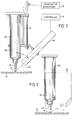
- bracket 11 holds adhesive dispenser 20 and sensor 30 for simultaneous vertical reciprocation, with the displacement being provided and monitored by a drive motor and encoder 10 according to a controller 12.
- optical sensor 30 which includes a laser diode light transmitter 31, solid state reflected light receiving detector 35, and their corresponding lenses 33 and 37.
- a typical sensor of this sort is manufactured by CyberOptics Corporation of Minneapolis, Minnesota as model LT-100.
- a transmitted beam of light 32 is focused as a small point of light (easily visible to an operator) onto the surface of the circuit board 14, and the reflected light beam 34 is focused onto a solid state detector 35.
- the reflected image moves along the length of the detector 35, as indicated in phantom lines in Figure 4, with the position of the image on the detector being indicative of the spacing between the sensor 30 and the top surface of circuit board 14.
- the sensor is able to measure by the position of the image on the detector and supply a trigger output signal at a preset distance from the reflecting surface.
- the plane defined by both the transmitted and reflected beams 32 and 34 may be at an angle of up to 45 degrees from a normal to the surface location being detected.
- sensing and distance measuring is particularly applicable for points on the surface underneath a reciprocating dispensing or depositing nozzle or the like.
- the transmitted beam 32 is hidden by the reflected beam 34 in Figure 1 and by tip 22 in Figure 2.
- the longitudinal axis 24 of adhesive dispenser 20 is positioned generally normal to the selected location on circuit board 14 at which an adhesive dot 16 is to be deposited. Positioning of the dispenser at the various selected locations on the circuit board is accomplished by moving the circuit board in directions parallel to the plane of the circuit board or, alternatively, by similarly moving the adhesive dispenser 20 to various locations of the circuit board.
- the drive motor 10 is actuated to advance the dispenser 20 and sensor 30 toward the board along longitudinal axis 24.
- the tip of nozzle 22 will pass a reference location which is a selectable distance above the surface of the circuit board so that a trigger location on detector 35 will receive the reflected image of the laser dot.
- the controller 12 is signaled to monitor the encoder and thus the distance that the tip of nozzle 22 travels past the reference location.
- the distance by which the tip of nozzle 22 travels past the reference location is programmable, and advancing of the tip may be halted a set distance past the reference location and thus at a set distance from the surface of the circuit board 14.
- the dispensing tip was spaced 0.008 inches from the board surface and glue was dispensed so as to bridge the gap between the board and the dispensing tip. Having forced the desired dosage of glue through the nozzle, the tip was retracted away from the surface of circuit board 14 and a dot of glue remained adhered to the board and separated from the tip resulting in a glue dot having a height of approximately 0.015 inches.
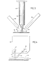
- this concept of sensing and providing a specific spacing of a tip from a surface of a circuit board may be utilized in retrieving components from a surface and/or placing components on a surface by means of a pick and place and head 40 which is reciprocatable along the longitudinal axis 44 and has a vacuum nozzle 42 for holding the components to the tip thereof.
- the particular spacing between the tip of nozzle 42 and the top surface of circuit board 14 may be selectable according to the thickness (or height as viewed in Figure 3) of the component 18 so as to avoid damage or unnecessary jarring or movement to the component or substrate during such picking or placing of the component.
- the optical sensor may be divided separately into a transmitter housing 46 and a receiver housing 48.
- This is particularly advantageous when the surface being sensed, i.e., the top surface of the component being picked up or the surface at the location where a component is to be placed, is particularly reflective or shiny and thus limits the angle at which an individual sensor housing 30 can be tilted away from the longitudinal axis of the dispenser or pick and place head with which it is utilized.
- a matte finish is generally preferred for accuracy when tilting the sensor as illustrated in Figures 1 and 2, with lesser angles of tilt being required for those surfaces which are less dull or more shiny and reflective.
- the reflective properties of the sensed surface do not present this problem and, yet, the device is still able to sense a point on the longitudinal axis of the pick and place head or depositing head.
- the senor 30, or at least the lens system thereof may be tiltable in concert with movement of the tip along the longitudinal axis of the head being used, thus obviating the need for the sensor to be attached for movement with the dispensing or pick and place head back and forth along a longitudinal axis.
- sources of light other than the laser can be utilized within the context of the invention.
- the laser projects a footprint onto the surface being sensed of only 0.001 inch, while providing greater accuracy and being less susceptible to color variations of the sensed surface than most other types of light.
- the particular sensor could be used to sense a location on the surface other than one which is in line with the longitudinal axis of the head, so as to act, in effect, as a non-contact "outrigger".
- a suitable controller for use in implementing the disclosed invention is the 8223B Satellite Controller manufactured by Universal Instruments Corporation, Binghamton, New York.
Abstract
Description
- The invention relates to depositing dots of adhesive at selected locations on the surface of a printed circuit board by sensing a reference spacing, between an adhesive dispensing nozzle tip advancing toward the substrate and each selected location on the substrate, and halting advance of the tip at a preferred distance from each selected location. The invention also may relate to spacing of the tip of a vacuum spindle of a pick and place machine for handling surface mountable device (SMD) components.
- Prior art devices generally include those which touch the depositing tip to the selected location on the substrate surface at which material is to be deposited and retract the tip away from the surface by a specific amount in order to attain a preferred spacing therebetween. With devices which sense contact with the surface by a reactive force, such as disclosed in U.S. Patent No. 4,661,368, calibration difficulties are encountered when used with flexible substrates, since contact with the substrate can cause it to flex before a required amount of reactive force is sensed via the tip. Thus, subsequent retraction of the tip, based on the sensed position of the surface, can result in insufficient spacing therebetween. Additionally, touching the board with the tip can cause jarring or movement of components and nicking of the fragile surfaces of some substrates.
- Other prior art surface locating devices utilize so called "outriggers" in sensing the appropriate spacing between a tip and a substrate by engaging and locating the substrate at a location other than the exact place at which deposition is to take place. Thus, a much larger "footprint" on the circuit board, involving the depositing tip and the sensing outrigger, is required. Additionally, this prior art does not compensate for circuit board warpage or surface waviness at the specific location at which depositing is to take place, since it senses a location on the substrate which is spaced from the specific location at which deposition is to occur.
- Thus, it is an objective of the invention to avoid contact with the board by the sensor while providing exact spacing between a dispensing tip or the like and each selected location on the board at which material is to be deposited.
- Further, it is an objective of the invention to avoid contact of the board by the depositing tip and thus reduce the time necessary in retracting the tip from the substrate prior to depositing.
- Additionally, it is an objective of the invention to avoid damaging the surface of the substrate and jarring or moving other components already mounted on the substrate.
- Also, it is an objective of the invention to sense the spacing between the substrate and depositing tip at the exact selected location for each deposited dose or component so as to minimize the footprint on the substrate.
- Still further, it is an objective of the invention to avoid the calibration difficulties inherent with "contact" type sensors when used with flexible substrates.
- Additionally, it is an objective of the invention to avoid spacing inaccuracies caused by board warpage or waviness inherent in use of devices which sense locations on the substrate other than the exact location where depositing is to take place.
-
- In a preferred embodiment of the invention, the tip of an adhesive dispensing nozzle is advanced toward a printed circuit board surface and the point on the circuit board at which a dot of adhesive is to be deposited is sensed when the tip is at a reference or trigger distance from the circuit board. At this time, the sensor signals a controller by a hardware interrupt so that the controller begins reading the output of an encoder. Thus, the controller monitors the amount of travel of the tip past the reference distance and instructs the drive motor to halt advance of the tip a particular distance past the reference distance. The resulting preferred spacing or distance of the tip from the specific location on the circuit board or substrate at which depositing is to take place equals the "reference distance" minus the "particular distance." The distance of advance of the tip past the reference distance is a selectable program variable of the controller.
- The novel features which are considered as characteristic for the invention are set forth in particular in the appended claims. The invention itself, however, in construction and method of operation, together with additional objectives and advantages thereof, will be best understood from the following detailed disclosure when read in connection with the accompanying drawings.
-
- Figure 1 is a front elevation, partially in schematic form, of an apparatus utilized in effecting the invention.
- Figure 2 is a right side elevation, with parts removed, of the device of Figure 1.
- Figure 3 is a front elevation, similar to that of Figure 1, illustrating another embodiment of the invention.
- Figure 4 is a schematic representation of the sensor and how it operates.
- Throughout the drawings, like numerals have been utilized where applicable.
- Referring to Figures 1 and 2, a dot of
glue 16 has been applied to printedcircuit board 14 vianozzle tip 22. As seen in Figure 1, bracket 11 holdsadhesive dispenser 20 andsensor 30 for simultaneous vertical reciprocation, with the displacement being provided and monitored by a drive motor andencoder 10 according to acontroller 12. - The reader's attention is directed to Figure 4 for a description of the operation of
optical sensor 30 which includes a laserdiode light transmitter 31, solid state reflectedlight receiving detector 35, and theircorresponding lenses - As seen in Figure 4, a transmitted beam of
light 32 is focused as a small point of light (easily visible to an operator) onto the surface of thecircuit board 14, and thereflected light beam 34 is focused onto asolid state detector 35. As the distance betweensensor 30 andcircuit board 14 lessens, the reflected image moves along the length of thedetector 35, as indicated in phantom lines in Figure 4, with the position of the image on the detector being indicative of the spacing between thesensor 30 and the top surface ofcircuit board 14. Thus, the sensor is able to measure by the position of the image on the detector and supply a trigger output signal at a preset distance from the reflecting surface. - As illustrated in Figures 1 and 2, of particular advantage to the instant invention is the fact that the plane defined by both the transmitted and
reflected beams beam 32 is hidden by thereflected beam 34 in Figure 1 and bytip 22 in Figure 2. - In operation, the
longitudinal axis 24 ofadhesive dispenser 20 is positioned generally normal to the selected location oncircuit board 14 at which anadhesive dot 16 is to be deposited. Positioning of the dispenser at the various selected locations on the circuit board is accomplished by moving the circuit board in directions parallel to the plane of the circuit board or, alternatively, by similarly moving theadhesive dispenser 20 to various locations of the circuit board. - Having positioned
dispenser 20 at a selected location above the circuit board, thedrive motor 10 is actuated to advance thedispenser 20 andsensor 30 toward the board alonglongitudinal axis 24. During such advancing toward the board, the tip ofnozzle 22 will pass a reference location which is a selectable distance above the surface of the circuit board so that a trigger location ondetector 35 will receive the reflected image of the laser dot. At that time, thecontroller 12 is signaled to monitor the encoder and thus the distance that the tip ofnozzle 22 travels past the reference location. With such an arrangement, the distance by which the tip ofnozzle 22 travels past the reference location is programmable, and advancing of the tip may be halted a set distance past the reference location and thus at a set distance from the surface of thecircuit board 14. - In practice, the dispensing tip was spaced 0.008 inches from the board surface and glue was dispensed so as to bridge the gap between the board and the dispensing tip. Having forced the desired dosage of glue through the nozzle, the tip was retracted away from the surface of
circuit board 14 and a dot of glue remained adhered to the board and separated from the tip resulting in a glue dot having a height of approximately 0.015 inches. - As illustrated in Figure 3, this concept of sensing and providing a specific spacing of a tip from a surface of a circuit board may be utilized in retrieving components from a surface and/or placing components on a surface by means of a pick and place and head 40 which is reciprocatable along the
longitudinal axis 44 and has avacuum nozzle 42 for holding the components to the tip thereof. Thus, the particular spacing between the tip ofnozzle 42 and the top surface ofcircuit board 14 may be selectable according to the thickness (or height as viewed in Figure 3) of the component 18 so as to avoid damage or unnecessary jarring or movement to the component or substrate during such picking or placing of the component. - As also seen in Figure 3, the optical sensor may be divided separately into a
transmitter housing 46 and areceiver housing 48. This is particularly advantageous when the surface being sensed, i.e., the top surface of the component being picked up or the surface at the location where a component is to be placed, is particularly reflective or shiny and thus limits the angle at which anindividual sensor housing 30 can be tilted away from the longitudinal axis of the dispenser or pick and place head with which it is utilized. A matte finish is generally preferred for accuracy when tilting the sensor as illustrated in Figures 1 and 2, with lesser angles of tilt being required for those surfaces which are less dull or more shiny and reflective. Of course, with the arrangement of Figure 3, the reflective properties of the sensed surface do not present this problem and, yet, the device is still able to sense a point on the longitudinal axis of the pick and place head or depositing head. - Having described the invention, it will be seen that the objectives set forth above, among those made apparent from the preceding description, are efficiently obtained and, since certain changes may be made in carrying out the above method and in the construction set forth without departing from the scope of the invention, it is intended that all matter contained in the above description or shown in the accompanying drawings shall be interpreted as illustrative and not in a limiting sense.
- For instance, it is considered within the context of the invention that the
sensor 30, or at least the lens system thereof may be tiltable in concert with movement of the tip along the longitudinal axis of the head being used, thus obviating the need for the sensor to be attached for movement with the dispensing or pick and place head back and forth along a longitudinal axis. It is also contemplated that sources of light other than the laser can be utilized within the context of the invention. However, the laser projects a footprint onto the surface being sensed of only 0.001 inch, while providing greater accuracy and being less susceptible to color variations of the sensed surface than most other types of light. It is also contemplated, although not preferred, that the particular sensor could be used to sense a location on the surface other than one which is in line with the longitudinal axis of the head, so as to act, in effect, as a non-contact "outrigger". - A suitable controller for use in implementing the disclosed invention is the 8223B Satellite Controller manufactured by Universal Instruments Corporation, Binghamton, New York.
- The following claims are intended to cover all of the generic and specific features of the invention herein described, and all statements of the scope of the invention which, as a matter of language, might be said to fall therebetween.
Claims (29)
advancing said tip toward said surface;
detecting, electrically separate from said surface and during said advancing, a reference spacing between said tip and a location on said surface in line with an axis of said advancing; and
halting advancing of said tip at a specified distance past said reference spacing, with said tip spaced said preferred distance from said surface location.
monitoring the advancing of said tip past said reference spacing.
preselecting said reference spacing and specified and preferred distances.
providing an optic system and reflecting light of said system from said surface location in order to detect said references spacing.
detecting a reference spacing between said tip and selected location, during relative advancing of said tip toward said location, without touching said surface with a means for detecting said spacing;
monitoring and controlling said advancing past said reference spacing; and
halting said advancing at a specified distance past said reference spacing such that said tip is positioned at said preferred distance from said location.
optically detecting said reference spacing.
moving said detecting means in concert with advancing of said tip in order to detect said reference spacing.
advancing a component holding portion of said head toward said location and detecting a reference spacing between a reference surface on said advancing portion and said selected location during said advancing;
monitoring and controlling said advancing past said reference spacing; and
halting said reference surface a preferred distance from said location sufficient for said picking and placing.
reflecting light from a surface of a component to be picked up in order to effect said detecting in preparation for picking up said component, said selected location being on said component surface; and
picking up said component.
reflecting light from a surface of a circuit board at said selected location in order to effect said detecting in preparation for placing said component, wherein said preferred distance substantially equals a height of said component; and
placing said component at said location.
means for advancing said tip toward said surface;
means for detecting, during said advancing, a reference spacing between said tip and a location on said surface in line with an axis of said advancing said detecting means being electrically separate from said surface at said location; and
means for halting advancing of said tip at a specified distance past said reference spacing, with said tip spaced preferred distance from said surface location.
means for monitoring the advancing of said tip past said reference spacing.
means for preselecting said reference spacing, and specified and preferred distances.
an optic system and means for reflecting light of said system from said surface location in order to detect said reference spacing.
means for detecting a reference spacing between said tip and selected location, during relative advancing of said tip toward said location, without touching said surface with a means for detecting said spacing;
means for monitoring and controlling said advancing past said reference spacing; and
means for halting said advancing at a specified distance past said reference spacing such that said tip is positioned at said preferred distance from said location.
means for optically detecting said reference spacing.
means for moving said detecting means in concert with advancing of said tip in order to detect said reference spacing.
means for advancing a component holding portion of said head toward said location and detecting a reference spacing between a reference surface on said advancing portion and said selected location during said advancing;
means for monitoring and controlling said advancing past said reference spacing; and
means for halting said reference surface a preferred distance from said location sufficient for said picking and placing.
means for reflecting light from a surface of a component to be picked up in order to effect said detecting in preparation for picking up said component, said selected location being on said component surface.
means for reflecting light from a surface of a circuit board at said selected location in order to effect said detecting in preparation for placing said component, wherein said preferred distance substantially equals a height of said component.
a laser diode generative of said light; and
a solid state detector receiving said reflected light.
advancing said tip toward said surface;
detecting, during said advancing, a reference spacing between said tip and a location on said surface in line with an axis of said advancing;
monitoring the advancing of said tip past said reference spacing; and
halting advancing of said tip at a specified distance past said reference spacing, with said tip spaced said preferred distance from said surface location.
advancing said tip toward said surface;
detecting, during said advancing, a reference spacing between said tip and a location on said surface in line with an axis of said advancing;
halting advancing of said tip at a specified distance past said reference spacing, with said tip spaced said preferred distance from said surface location; and
preselecting said reference spacing and specified and preferred distances.
providing an optic system;
advancing said tip toward said surface;
detecting, during said advancing, a reference spacing between said tip and a location on said surface in line with an axis of said advancing by reflecting light of said system from said surface location; and
halting advancing of said tip at a specified distance past said reference spacing, with said tip spaced said preferred distance from said surface location.
means for advancing said tip toward said surface;
means for detecting, during said advancing, a reference spacing between said tip and a location on said surface in line with an axis of said advancing;
means for monitoring the advancing of said tip past said reference spacing; and
means for halting advancing of said tip at a specified distance past said reference spacing, with said tip spaced said preferred distance from said surface location.
means for advancing said tip toward said surface;
means for detecting, during said advancing, a reference spacing between said tip and a location on said surface in line with an axis of said advancing;
means for halting advancing of said tip at a specified distance past said reference spacing, with said tip spaced said preferred distance from said surface location; and
means for preselecting said reference spacing, and specified and preferred distances.
means for advancing said tip toward said surface;
means for detecting, during said advancing, a reference spacing between said tip and a location on said surface in line with an axis of said advancing, said detecting means comprising an optic system and means for reflecting light of said system from said surface location; and
means for halting advancing of said tip at a specified distance past said reference spacing, with said tip spaced said preferred distance from said surface location.
advancing said tip toward said surface;
detecting, during said advancing, a reference spacing between said tip and a point on said surface in line with an axis of said advancing; and
halting advancing of said tip at a specified distance past said reference spacing, with said tip spaced said preferred distance from said point.
means for advancing said tip toward said surface;
means for detecting, during said advancing, a reference spacing between said tip and a point on said surface in line with an axis of said advancing; and
means for halting advancing of said tip at a specified distance past said reference spacing, with said tip spaced said preferred distance from said point.
Applications Claiming Priority (2)
| Application Number | Priority Date | Filing Date | Title |
|---|---|---|---|
| US43623 | 1987-04-28 | ||
| US07/043,623 US4762578A (en) | 1987-04-28 | 1987-04-28 | Non-contact sensing and controlling of spacing between a depositing tip and each selected depositing location on a substrate |
Publications (2)
| Publication Number | Publication Date |
|---|---|
| EP0289421A2 true EP0289421A2 (en) | 1988-11-02 |
| EP0289421A3 EP0289421A3 (en) | 1990-07-25 |
Family
ID=21928076
Family Applications (1)
| Application Number | Title | Priority Date | Filing Date |
|---|---|---|---|
| EP88401033A Ceased EP0289421A3 (en) | 1987-04-28 | 1988-04-27 | Non-contact sensing and controlling of spacing between a depositing tip and each selected depositing location on a substrate |
Country Status (4)
| Country | Link |
|---|---|
| US (1) | US4762578A (en) |
| EP (1) | EP0289421A3 (en) |
| JP (1) | JPH01105106A (en) |
| CA (1) | CA1296083C (en) |
Cited By (7)
| Publication number | Priority date | Publication date | Assignee | Title |
|---|---|---|---|---|
| EP0314012A2 (en) * | 1987-10-29 | 1989-05-03 | Siemens Aktiengesellschaft | Method and apparatus for controlled applying of adhesive spots |
| DE3928864A1 (en) * | 1989-08-31 | 1991-03-07 | Winkler Duennebier Kg Masch | METHOD AND DEVICE FOR PRODUCING MULTI-LAYERED CONFECTIONERY |
| EP0427362A2 (en) * | 1989-11-07 | 1991-05-15 | Helmuth Dipl.-Ing. Klatt | Method and device for metering and applying a pasty fluid |
| GB2246211A (en) * | 1990-06-14 | 1992-01-22 | Sony Corp | Electronic component mounting apparatus |
| EP1328009A2 (en) * | 2002-01-15 | 2003-07-16 | Robert Bosch Gmbh | Apparatus for mounting an element on a substrate |
| EP1432013A1 (en) * | 2002-12-18 | 2004-06-23 | Esec Trading S.A. | Semiconductor-mounting apparatus for dispensing an adhesive on a substrat |
| WO2005107355A2 (en) * | 2004-04-23 | 2005-11-10 | Speedline Technologies, Inc. | Imaging and inspection system for a dispenser and method for same |
Families Citing this family (39)
| Publication number | Priority date | Publication date | Assignee | Title |
|---|---|---|---|---|
| JPH07105407B2 (en) * | 1987-12-28 | 1995-11-13 | 株式会社東芝 | Die bonding method |
| US4857133A (en) * | 1988-05-20 | 1989-08-15 | Hybond, Inc. | Method and apparatus for bonding with consistent uniform bond thickness |
| US5110615A (en) * | 1990-01-31 | 1992-05-05 | Asymptotic Technologies, Inc. | Method for dispensing viscous materials a constant height above a workpiece surface |
| US5052338A (en) * | 1990-01-31 | 1991-10-01 | Asymptotic Technologies, Inc. | Apparatus for dispensing viscous materials a constant height above a workpiece surface |
| US5147462A (en) * | 1990-02-16 | 1992-09-15 | Alcan Aluminum Corporation | Apparatus for automatic film thickness control |
| US5119759A (en) * | 1990-09-24 | 1992-06-09 | International Business Machines Corporation | Apparatus for solder nozzle height sensing |
| US5148963A (en) * | 1990-09-24 | 1992-09-22 | International Business Machines Corporation | Method for solder nozzle height sensing |
| US5151377A (en) * | 1991-03-07 | 1992-09-29 | Mobil Solar Energy Corporation | Method for forming contacts |
| JP2740588B2 (en) * | 1991-07-24 | 1998-04-15 | 日立テクノエンジニアリング株式会社 | Coating and drawing equipment |
| US5320250A (en) * | 1991-12-02 | 1994-06-14 | Asymptotic Technologies, Inc. | Method for rapid dispensing of minute quantities of viscous material |
| US5324359A (en) * | 1992-02-25 | 1994-06-28 | Nouvas Manufacturing Technology Co. | Material deposition device |
| US5298073A (en) * | 1992-02-28 | 1994-03-29 | Libbey-Owens-Ford Co. | Two sensor for determining spacing between surfaces |
| US5547537A (en) * | 1992-05-20 | 1996-08-20 | Kulicke & Soffa, Investments, Inc. | Ceramic carrier transport for die attach equipment |
| EP0582086B2 (en) * | 1992-07-01 | 1999-01-13 | Yamaha Hatsudoki Kabushiki Kaisha | Method for mounting components and an apparatus therefor |
| US5415693A (en) * | 1992-10-01 | 1995-05-16 | Hitachi Techno Engineering Co., Ltd. | Paste applicator |
| US5489337A (en) * | 1993-01-28 | 1996-02-06 | Kabushiki Kaisha Toshiba | Apparatus for applying organic material to semiconductor wafer in which the nozzle opening adjusts in response to data |
| JPH0778233A (en) * | 1993-09-07 | 1995-03-20 | Nordson Kk | Detection |
| DE4334745C5 (en) * | 1993-10-12 | 2007-09-20 | Focke & Co.(Gmbh & Co. Kg) | Device for applying glue |
| US5589940A (en) * | 1994-12-21 | 1996-12-31 | Hughes Electronics | Apparatus for measuring the curvature of a surface using moveable reflecting and focusing elements |
| US5902445A (en) * | 1995-09-11 | 1999-05-11 | Ast Holding, Ltd. | Apparatus for bonding with a meltable composition |
| JP3697315B2 (en) | 1996-05-13 | 2005-09-21 | 松下電器産業株式会社 | Adhesive applicator |
| JP3275202B2 (en) * | 1996-08-30 | 2002-04-15 | 東京エレクトロン株式会社 | Thin film forming equipment |
| US6093251A (en) * | 1997-02-21 | 2000-07-25 | Speedline Technologies, Inc. | Apparatus for measuring the height of a substrate in a dispensing system |
| JP2002500099A (en) * | 1998-01-09 | 2002-01-08 | エフエイスター、リミティド | Moving head, coating apparatus and method |
| JP4358991B2 (en) | 1998-08-04 | 2009-11-04 | サイバーオプティクス コーポレーション | Enhanced sensor |
| US6866881B2 (en) * | 1999-02-19 | 2005-03-15 | Speedline Technologies, Inc. | Dispensing system and method |
| DE19938328C2 (en) * | 1999-08-12 | 2003-10-30 | Daimler Chrysler Ag | Method and device for the automated application of an adhesive bead |
| US6706315B2 (en) * | 2001-09-17 | 2004-03-16 | Xerox Corporation | Coating process for coating die with laser position sensors |
| US6711466B2 (en) * | 2002-01-07 | 2004-03-23 | International Business Machines Corporation | Method and system for maintaining a desired distance between a dispenser and a surface |
| KR100540633B1 (en) * | 2003-06-20 | 2006-01-11 | 주식회사 탑 엔지니어링 | Paste Dispenser and Method for Controlling the same |
| JP4501382B2 (en) * | 2003-09-11 | 2010-07-14 | 株式会社豊田自動織機 | Defogger wire coating device |
| US7955865B2 (en) * | 2004-06-09 | 2011-06-07 | The University Of British Columbia | Reagent delivery apparatus and methods |
| JP2011514234A (en) | 2007-12-31 | 2011-05-06 | エグザテック・リミテッド・ライアビリティー・カンパニー | Apparatus and method for printing on a three-dimensional object |
| EP2276862B1 (en) * | 2008-04-16 | 2023-12-20 | Imbox Protection A/S | Method and apparatus for impregnation of items |
| US20100108256A1 (en) * | 2008-11-05 | 2010-05-06 | Western Digital Technologies, Inc. | Closed loop control of adhesive dot characteristics |
| DE102009020785A1 (en) * | 2009-05-11 | 2010-11-25 | Marco Systemanalyse Und Entwicklung Gmbh | Valve |
| US20120196029A1 (en) * | 2011-01-27 | 2012-08-02 | Exatec, Llc | Apparatus and method of forming a uniform grid line |
| GB2556991A (en) * | 2016-09-30 | 2018-06-13 | Herotec Gmbh Flachenheizung | Bodensystem |
| CN111001534B (en) * | 2019-12-13 | 2021-05-04 | 青岛歌尔智能传感器有限公司 | Dispensing method and dispensing device |
Citations (3)
| Publication number | Priority date | Publication date | Assignee | Title |
|---|---|---|---|---|
| US4204146A (en) * | 1978-06-01 | 1980-05-20 | Barbedienne Roger Serge | Servo-control method and device |
| FR2564349A1 (en) * | 1984-05-17 | 1985-11-22 | Benedite Claude Laser Tech | Laser-ray machine head with automatic correction of the position of the focal plane |
| EP0216601A2 (en) * | 1985-09-18 | 1987-04-01 | Universal Instruments Corporation | Surface locating and dispensed dosage sensing method and apparatus |
Family Cites Families (3)
| Publication number | Priority date | Publication date | Assignee | Title |
|---|---|---|---|---|
| NL274071A (en) * | 1961-01-27 | |||
| US3809308A (en) * | 1969-08-16 | 1974-05-07 | Messer Griesheim Gmbh | Machine for maintaining constant the distance of a cutting or welding torch from the work piece |
| US4485387A (en) * | 1982-10-26 | 1984-11-27 | Microscience Systems Corp. | Inking system for producing circuit patterns |
-
1987
- 1987-04-28 US US07/043,623 patent/US4762578A/en not_active Expired - Lifetime
-
1988
- 1988-04-22 CA CA000564948A patent/CA1296083C/en not_active Expired - Lifetime
- 1988-04-27 EP EP88401033A patent/EP0289421A3/en not_active Ceased
- 1988-04-27 JP JP63102850A patent/JPH01105106A/en active Pending
Patent Citations (3)
| Publication number | Priority date | Publication date | Assignee | Title |
|---|---|---|---|---|
| US4204146A (en) * | 1978-06-01 | 1980-05-20 | Barbedienne Roger Serge | Servo-control method and device |
| FR2564349A1 (en) * | 1984-05-17 | 1985-11-22 | Benedite Claude Laser Tech | Laser-ray machine head with automatic correction of the position of the focal plane |
| EP0216601A2 (en) * | 1985-09-18 | 1987-04-01 | Universal Instruments Corporation | Surface locating and dispensed dosage sensing method and apparatus |
Non-Patent Citations (1)
| Title |
|---|
| IEEE 1986 ULTRASONICS SYMPOSIUM PROCEEDINGS vol. 1, November 1986, USA pages 539 - 543; J.S. SHOENWALD ET AL: "APPLICATION OF ACOUSTICS TO CONTROL KINEMATIC AND DYNAMIC BEHAVIOR IN ROBOTS" * |
Cited By (14)
| Publication number | Priority date | Publication date | Assignee | Title |
|---|---|---|---|---|
| EP0314012A2 (en) * | 1987-10-29 | 1989-05-03 | Siemens Aktiengesellschaft | Method and apparatus for controlled applying of adhesive spots |
| EP0314012A3 (en) * | 1987-10-29 | 1989-12-20 | Bernhard Dipl.-Ing. Martin | Method and apparatus for controlled applying of adhesive spots |
| DE3928864A1 (en) * | 1989-08-31 | 1991-03-07 | Winkler Duennebier Kg Masch | METHOD AND DEVICE FOR PRODUCING MULTI-LAYERED CONFECTIONERY |
| DE3928864C2 (en) * | 1989-08-31 | 1998-11-26 | Winkler Und Duennebier Sueswar | Method and device for producing multilayered confectionery |
| EP0427362A2 (en) * | 1989-11-07 | 1991-05-15 | Helmuth Dipl.-Ing. Klatt | Method and device for metering and applying a pasty fluid |
| EP0427362A3 (en) * | 1989-11-07 | 1992-01-02 | Helmuth Dipl.-Ing. Klatt | Method and device for metering and applying a pasty fluid |
| GB2246211B (en) * | 1990-06-14 | 1994-02-16 | Sony Corp | Electronic component mounting apparatus |
| GB2246211A (en) * | 1990-06-14 | 1992-01-22 | Sony Corp | Electronic component mounting apparatus |
| EP1328009A2 (en) * | 2002-01-15 | 2003-07-16 | Robert Bosch Gmbh | Apparatus for mounting an element on a substrate |
| EP1328009A3 (en) * | 2002-01-15 | 2005-08-03 | Robert Bosch Gmbh | Apparatus for mounting an element on a substrate |
| EP1432013A1 (en) * | 2002-12-18 | 2004-06-23 | Esec Trading S.A. | Semiconductor-mounting apparatus for dispensing an adhesive on a substrat |
| WO2005107355A2 (en) * | 2004-04-23 | 2005-11-10 | Speedline Technologies, Inc. | Imaging and inspection system for a dispenser and method for same |
| WO2005107355A3 (en) * | 2004-04-23 | 2006-03-23 | Speedline Technologies Inc | Imaging and inspection system for a dispenser and method for same |
| US7404861B2 (en) | 2004-04-23 | 2008-07-29 | Speedline Technologies, Inc. | Imaging and inspection system for a dispenser and method for same |
Also Published As
| Publication number | Publication date |
|---|---|
| EP0289421A3 (en) | 1990-07-25 |
| US4762578A (en) | 1988-08-09 |
| JPH01105106A (en) | 1989-04-21 |
| CA1296083C (en) | 1992-02-18 |
Similar Documents
| Publication | Publication Date | Title |
|---|---|---|
| US4762578A (en) | Non-contact sensing and controlling of spacing between a depositing tip and each selected depositing location on a substrate | |
| JP4824698B2 (en) | Method for adjusting nozzle clearance of liquid coating apparatus and liquid coating apparatus | |
| US4688184A (en) | System for measuring three-dimensional coordinates | |
| US5566447A (en) | Pick-up point correction device for mounter | |
| US6678062B2 (en) | Automated system with improved height sensing | |
| GB2183820A (en) | Electronic component placement | |
| US5619328A (en) | Component mounter and recognition method | |
| EP0493908B1 (en) | Monitoring the condition of a rotary tool | |
| EP0416878B1 (en) | Electronic component apparatus and method of mounting electronic component | |
| US6955284B2 (en) | Device for positioning a tool in relation to a workpiece | |
| EP3764763A1 (en) | Component mounting system | |
| US20020138977A1 (en) | Mounting apparatus of electronic parts and mounting methods of the same | |
| KR20010085492A (en) | Apparatus and method for mounting electronic component | |
| JP3372799B2 (en) | Paste coating machine | |
| JP2000114787A (en) | Electronic part mounter and mounting method | |
| EP0808090A1 (en) | Adjustment device for electronic part installation apparatus and method of adjustment thereof | |
| JP3520205B2 (en) | Paste application method and paste application machine | |
| JP3806661B2 (en) | Paste application method and paste applicator | |
| JP2007075772A (en) | Paste applicator and paste application method | |
| JP2003289199A (en) | Working system for board | |
| US5444205A (en) | Method of and apparatus for electro-erosive machining | |
| US4914290A (en) | Method and apparatus for measuring of microdistances | |
| US6400459B1 (en) | Methods and apparatus for using optical sensors in component replacement heads | |
| JPH08228097A (en) | Method and apparatus for mounting part | |
| JP4296029B2 (en) | Electronic component mounting equipment |
Legal Events
| Date | Code | Title | Description |
|---|---|---|---|
| PUAI | Public reference made under article 153(3) epc to a published international application that has entered the european phase |
Free format text: ORIGINAL CODE: 0009012 |
|
| AK | Designated contracting states |
Kind code of ref document: A2 Designated state(s): DE FR GB NL |
|
| PUAL | Search report despatched |
Free format text: ORIGINAL CODE: 0009013 |
|
| RHK1 | Main classification (correction) |
Ipc: B23Q 15/24 |
|
| AK | Designated contracting states |
Kind code of ref document: A3 Designated state(s): DE FR GB NL |
|
| 17P | Request for examination filed |
Effective date: 19900809 |
|
| 17Q | First examination report despatched |
Effective date: 19920409 |
|
| STAA | Information on the status of an ep patent application or granted ep patent |
Free format text: STATUS: THE APPLICATION HAS BEEN REFUSED |
|
| 18R | Application refused |
Effective date: 19930722 |