EP0288564B1 - Device for detecting vehicle on track - Google Patents
Device for detecting vehicle on track Download PDFInfo
- Publication number
- EP0288564B1 EP0288564B1 EP86905931A EP86905931A EP0288564B1 EP 0288564 B1 EP0288564 B1 EP 0288564B1 EP 86905931 A EP86905931 A EP 86905931A EP 86905931 A EP86905931 A EP 86905931A EP 0288564 B1 EP0288564 B1 EP 0288564B1
- Authority
- EP
- European Patent Office
- Prior art keywords
- signal
- circuit
- level
- output
- phase
- Prior art date
- Legal status (The legal status is an assumption and is not a legal conclusion. Google has not performed a legal analysis and makes no representation as to the accuracy of the status listed.)
- Expired - Lifetime
Links
- 239000004065 semiconductor Substances 0.000 claims description 4
- 230000001131 transforming effect Effects 0.000 claims description 2
- 238000001514 detection method Methods 0.000 description 11
- 239000003990 capacitor Substances 0.000 description 10
- 230000010355 oscillation Effects 0.000 description 7
- 238000010586 diagram Methods 0.000 description 6
- 230000015572 biosynthetic process Effects 0.000 description 5
- 230000000694 effects Effects 0.000 description 4
- 230000005281 excited state Effects 0.000 description 3
- 230000005540 biological transmission Effects 0.000 description 2
- 230000007547 defect Effects 0.000 description 2
- 230000003321 amplification Effects 0.000 description 1
- 230000008033 biological extinction Effects 0.000 description 1
- 239000000470 constituent Substances 0.000 description 1
- 230000008094 contradictory effect Effects 0.000 description 1
- 230000008878 coupling Effects 0.000 description 1
- 238000010168 coupling process Methods 0.000 description 1
- 238000005859 coupling reaction Methods 0.000 description 1
- 230000000977 initiatory effect Effects 0.000 description 1
- 230000010354 integration Effects 0.000 description 1
- 238000012423 maintenance Methods 0.000 description 1
- 238000000034 method Methods 0.000 description 1
- 238000003199 nucleic acid amplification method Methods 0.000 description 1
- 230000011664 signaling Effects 0.000 description 1
Images

Classifications
-
- B—PERFORMING OPERATIONS; TRANSPORTING
- B61—RAILWAYS
- B61L—GUIDING RAILWAY TRAFFIC; ENSURING THE SAFETY OF RAILWAY TRAFFIC
- B61L1/00—Devices along the route controlled by interaction with the vehicle or train
- B61L1/18—Railway track circuits
- B61L1/181—Details
- B61L1/187—Use of alternating current
Definitions
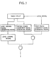
- the present invention relates to a vehicle detecting apparatus for detecting whether or not a vehicle is present on a railroad or on rails in a marshaling yard.
- a railway relay in which rails are used as parts of a circuit, a short circuit is formed between two rails through wheels and a wheel shaft when a train is present on a track and the change of the voltage by the formation of the short circuit is read to actuate the relay and detect the presence or absence of the vehicle. More specifically, a predetermined length of the track is divided into sections, and rails of the specific section are utilized as parts of an electric circuit. If a short circuit is formed between the rails by a train present on the track, the presence of the vehicle in this section is detected by an electromagnetic track relay. Various safety devices of the railway signal system are controlled by this detection signal. As one of the railway relay of this type, there is known an alternating current railway relay which is actuated by an alternating current flowing in rails.
- an alternating current railway relay disclosed in a pamphlet published by LM ERICSSON Signalling Systems Department, Sweden is driven and controlled by utilizing a semiconductor switch.
- this alternating railway relay comprises an electric circuit including a first transformer for the input of an alternating current local signal applied as a reference signal to rails of the specific section, a second transformer for the input of a track signal, which is connected to rails on which a train runs, a third transformer for putting out a train detection judgement signal, a plurality of thyristors, a plurality of diodes and an output relay to be actuated based on the detection signal of the third transformer.
- the phase of the track signal for the specific closed section is made different by ⁇ from that for the adjacent precedent section.
- the phase of the track signal of the specific section becomes in agreement with the phase of the local signal and the voltage level of the track signal is maintained at a level above a predetermined value because of formation of no short circuit between the rails, that is, only when these two conditions are satisfied, an alternating current output is generated on the secondary side of the third transformer, and a signal of the absence of a train is put out to excite the railway relay.
- the phase of the track signal is made different in respective track sections, and the presence of a vehicle is informed based on the result of the judgement of the voltage level and phase of the track signal.
- the phase of the local signal and track signal it is most advantageous to detect the zero level at which the polarity of the signal is changed.
- the threshold level for receipt of signals is elevated to broaden the noise-insensitive region.
- the judgement of the phase is precise when the alternating current signals, that is, the track signal and local signals, are close to the zero points, because the judgement is hardly influenced by changes of amplitudes of the signals.
- the output relay is operated by the on-off operation of the local signal by the thyristor through the first and third transformers, and the conventional apparatus cannot be integrated as a detection apparatus having so-called intelligent functions necessary for a train detection sensor, such as the function of a precise level judgement and the filter function.
- the level judgement of the track signal becomes impossible and even if a train is present and the track signal is at the low level, the circuit is constructed and an output is generated in the third transformer, with the result that no fail-safe effect is attained. This is a defect which is essentially caused because the voltage exciting the output relay depends on the frequency of the input signal, that is, the third transformer directly treats the frequency of the input signal.
- the track circuits are a kind of coded track circuits wherein one of rate codes is modulated by a local signal, the modulated code signal is delivered from a code transmitter through a typical track section and received by a receiver, the received signal which is applied as a track signal is demodulated to attain the code signal, a level judgement and a phase judgement of the demodulated code signal are performed and then existence or nonexistence of a vehicle on the track section is detected based on the both judgements.
- DE-A-2047147 describes an apparatus which includes the features of the pre-characterising part of claim 1.
- Another object of the present invention is to provide a vehicle detecting apparatus having a fail-safe effect.
- an apparatus for detecting a vehicle on a track which comprises a track circuit in which a local signal which is an alternating current voltage signal of a specific frequency is applied to a specific closed section of a pair of rails, and a track signal whose voltage varies according to the presence or absence of a vehicle on the rails, is produced, phase judgement means for judging whether the phase of the local signal and the track signal are the same, and level judgement means for judging whether a voltage level of the track signal is higher than a predetermined value and which produces a signal indicative of the absence of a vehicle on the pair of rails in the specific closed section only when both the local signal and the track signal are of the same phase and the level of the track signal is higher than the predetermined value, characterised in that the apparatus comprises:
- the first and second logical product circuits may be constructed by a single logical product computing oscillating circuit.
- the judgement of the phases can be performed at a low level to reduce the influences of variations of the amplitude and the level judgement can be performed at a high level to improve the noise resistance.
- the local input signal can be subjected to integration processing.
- a vehicle 1 runs on two rails 2 and 3 in the direction indicated by the arrow.
- the rails 2 and 3 are divided into a plurality of sections such as a specific section 4 and a section 5 rear with respect to the direction of advance of the vehicle.
- a transmission signal which is an alternating current reference voltage Vl (this signal is simultaneously fed to the reception side and acts as a local signal Sl ) is applied to the rails of each of the block sections 4 and 5.
- the rails 2 and 3 are utilized as parts of the circuit and the voltage Vt between the rails 2 and 3 is put out as a track signal St for reception.
- This circuit is known as the alternating current track circuit.
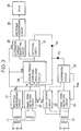
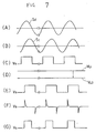
- the transmission signal of the track is a sine wave alternating current signal shown in Fig. 7-A and is put in a rectifying smoothening circuit 21 and a wave form rectifying circuit 22 through a transformer 11.
- the rectifying smoothening circuit 21 is a known circuit for rectifying and smoothening an alternating current signal arid forming a direct current output power source Vs.
- the wave form rectifying circuit 22 acts as the first phase judgement signal generating means and is a known circuit, for example, a Schmitt circuit for rectifying a sine wave local signal to a rectangular wave as shown in Fig. 7-C. By these circuits, a rectangular wave phase judgement signal vibrating with the reference voltage level being as the center is obtained.
- the track signal St is put in a level judging signal 23 and a wave form rectifying circuit 24 through a second transformer 12.
- the level judging circuit 23 is a circuit for detecting whether or not a voltage obtained by transforming the track signal St by the transformer 12 acting as the level judgement signal generating means, that is , a level judging signal, is higher than a predetermined value.
- this circuit comprises a level detecting circuit such as a Schmitt circuit and a known voltage doubling half-wave rectifying circuit for rectifying the output of this detecting circuit, which includes, for example, capacitors C1 and C2 and diodes D1 and D2, as shown in Fig. 4.
- a relatively high threshold level is set in the Schmitt circuit.
- the voltage doubling half-wave rectifying circuit rectifies and smoothens the alternating current voltage put out from the Schmitt circuit by the diode D2 and the capacitor C2 through the coupling capacitor C1 and the clamp diode D1 and a rectified output is obtained from an output terminal D.
- the voltage doubling half-wave rectifying circuit has such a fail-safe structure that at the time of a trouble such as disconnection, no rectified output is obtained (a known four-terminal capacitor which generates no output at the time of disconnection of a terminal is shown as the capacitor C2).
- the direct current voltage Vs of the rectifying smoothening circuit 21 is put in the rectifying circuit.
- the diode D1 is constructed so that a computing oscillator of the subsequent stage is oscillated by the output of the rectifying circuit by clamping the input signal from the capacitor C1 to this input power source Vs.
- the wave form rectifying circuit 24 has a threshold level sufficiently lower than the track signal St put in the circuit 24. Accordingly, a wave-rectified output which changes substantially at the zero point of the track signal St can be produced.
- a differential circuit 25 comprises, for example, a capacitor C3 and a resistor R1, as shown in Fig. 5, and has such a known structure that the reference voltage level is set at the above-mentioned level Vs. Thus, the phase of the track signal is generated substantially at the zero point (reference voltage level).
- the phase signal of the track signal only a positive signal is put into an input terminal c of a three-input logical product circuit 26 through a diode D4.
- a structure capable of performing a desired operation may be formed even by omitting the diode D4.
- the logical product circuit 26 has three input terminals a, b and c, and this circuit receives the output of the wave form rectifying circuit 22 at the input terminal a and the output of the level detecting circuit 23 at the input terminal b.
- the logical product circuit 26 is a logical product computing oscillating circuit shown in Fig.
- the logical product computing oscillating circuit generates an oscillating output when all of the inputs at the input terminals a, b and c are higher than the power source voltage Vs and has a fail-safe structure in which when a constituent element of the circuit gets out of order, oscillation is impossible and therefore, no output is generated at the time of a trouble,
- the type of the transistor is changed to NPN from PNP and the direction of the diode is reversed.
- Transistors Tr1 and Tr2 are connected to each other through an attenuation resistor R6, and the collector of the transistor Tr2 is connected to the base of a transistor Tr3 through a level shifting Zener diode ZD1 and the connecting point between a Zener diode ZD2 connected to the collector of the transistor Tr3 and a resistor R4 is connected to the base of the transistor Tr1 through a resistor R5.
- R2 and R3 represent collector resistors
- R7 represents a resistor on the leak current side, that is, a resistor for flowing of a leak current of the base of the transistor Tr3
- Vs represents an input power source
- C represents an output terminal.
- the operation of the transistors Tr1 through Tr3 is not reversed and the oscillation is stopped. Also when a trouble such as disconnection is caused in the circuit, the oscillation is stopped and no oscillating output is generated at the output terminal C.
- the Zener voltages VZD2 and VZD2 of the Zener diodes ZD1 and ZD2 be selected to satisfy the condition of VZD2 ⁇ Vs ⁇ VZD1.
- a computing oscillator of a high output can be constructed by connecting a known amplifier to the input terminal.
- the level judging circuit 23 and the rectifying circuit 27 described hereinafter may comprise, for example, the voltage doubling half-wave rectifying circuit, and this voltage doubling half-wave rectifying circuit and the logical product computing oscillator shown in Fig. 6 may be a known fail-safe logical product circuit in which no output is produced unless input signals are applied to all of the input terminals a, b and c, disclosed in, for example, Japanese Utility Model Application Laid-Open Specification No. 4764/82 or Japanese patent Publication No. 38211/76.
- the rectified output of the rectifying circuit 27 for rectifying the output of the logical product computing oscillating circuit 26 is fed back to the input terminal c, in which the output of the differential circuit 25 is put, through the diode D3.
- An alternating current amplifying circuit 28 amplifies the oscillating output of the logical product computing oscillating circuit 26, and the amplified output is rectified by a rectifying smoothening circuit 29 to drive a trade relay 30, as in the conventional apparatus.
- the above-mentioned transformer 12, wave form rectifying circuit 24, differential circuit 25, rectifying circuit 27 and diodes D3 and D4 constitute the second phase judgement signal generating means, and the wave rectifying circuit 24 and differential circuit 25 constitute the means for detecting the zero point of the track signal.
- the alternating current local signal shown in Fig. 7-A is put in the rectifying smoothening circuit 21 and wave form rectifying circuit 22 through the first transformer 11.
- the rectifying smoothening circuit 21 there is generated the direct current output Vs to be used as the power for driving the level detecting circuit 23, wave form rectifying circuits 22 and 24, amplifying circuit 28, logical product computing oscillating circuit 26 and track relay 30.
- a rectangular wave shown in Fig. 7-C is generated as the phase judging signal. This phase judging signal oscillates with the reference voltage level (corresponding to the zero point of the track signal) being as the center.
- the track signal St put in the second transformer 12 from the rails 2 and 3 has a shape of a sine save as shown in Fig. 7-B.
- the track signal St is put in the level judging circuit 23 and wave form rectifying circuit 24, and a rectified direct current output VL1 for detecting a level higher than a predetermined value, as shown in Fig. 7-D, is produced from the former circuit.
- a rectangular wave as shown in Fig. 7-E is put out from the latter circuit and a differential pulse as shown in Fig. 7-F is put out from the differential circuit 25.
- each of the outputs of the wave form rectifying circuits 22 and 24, level judging circuit 23 and differential circuit 25 is put out in the state where the direct current output Vs of the rectifying smoothening circuit 21 is over-lapped.
- each of positive pulses of the wave rectifying circuit 22, level judging circuit 23 and differential circuit 25 to be put into the input terminals a, b and c of the logical product computing oscillating circuit 26, respectively, has an input level higher than the power source voltage Vs at which initiation of the oscillation is possible,
- the phase judgement condition (the local signal and the track signal are of the same phase) is established (first logical product)
- the logical product (second logical product) of this established condition and the already established level judgement condition (the voltage level of the track signal is higher than a predetermined value) is established and oscillation is initiated in the logical product computing oscillating circuit 26.
- the oscillating output of the computing oscillating circuit 26 is put in the alternating current amplifying circuit 28 and is simultaneously rectified by the rectifying circuit 27 and fed back to the input terminal c through the diode D3 to self-retain the output of the computing oscillator 26 until the phase signal on the local signal side (Fig. 7-C) falls, whereby amplification of the pulse width is effected (see Fig. 7-G).
- the diode D3 prevents extinction of the differential pulse at the capacitor C2 of the rectifying circuit 27.
- the pulse width-amplified output, shown in Fig. 7-G, of the computing oscillating circuit 26 is amplified by the alternating amplifying circuit 28, rectified by the rectifying smoothening circuit 29 and supplied to the relay 30 to retain the relay 30 in the excited state. Namely, the absence of a train in the track circuit is informed.
- the track signal St put out from the wave rectifying circuit 24 is differentiated and the positive differential pulse is put in the computing oscillating circuit 26, whereby the oscillating output is self-retained and maintained.
- the phase to be judged is simultaneously determined.
- the judged value of the phase is changed with this change of the voltage level. This change becomes great as the set value for the judgement of the level is large.
- the conventional apparatus is disadvantageous in that if increase of the precision of the level judgement is intended, the precision of the phase judgement is reduced and if maintenance of a high precision of the phase judgement is intended, the precision of the level judgement is reduced.
- the set value for the level judgement can be increased, and the phase judgement can always be done at the point where the phase judging signal crosses the reference voltage, that is, at the point (zero point) where the track signal is changed to the positive value from the negative value. Accordingly, the detection precision can be elevated and the reliability can be improved.
- known fail-safe logical product computing oscillating circuit 26, level judging circuit 23, rectifying circuit 27, alternating current amplifying circuit 28 and differential circuit 25 are used, a fail-safe structure is realized in the detecting apparatus.
- the computing oscillating circuit 26 is not self-retained if the diode D3 is opened, a power sufficient to excite the relay 30 is not obtained, and since the differential pulse is absorbed in the capacitor C2 and no signal is put in the input terminal c of the computing oscillating circuit 26 if a short circuit is formed, a fail-safe effect is attained.
- the logical product of the level judgement and the phase judgement is made by one logical product circuit, but the present invention is not limited to this structure. Namely, there may be adopeted a structure in which the phase judgement is carried out by using a fail-safe logical product circuit, the relay 30 is driven by this judgement signal and the contact output of the relay driven by the output of the level judging circuit 23 is connected in series to the contact output of the relay 30.
- the rectifying circuit is used as the level judging circuit 23, it is obvious that the output may be rectified by using a known level detector of the alternating current input type.
- the input level of the track signal is stable, it is obvious that an alternating current output from the level detecting circuit of the level judging circuit 23, as indicated by a dot line in Fig. 3, can be utilized instead of the wave rectifying circuit 24. Furthermore, if the input detection level of the logical product circuit is made equal to the judgement level of the track signal, the logical product circuit can be utilized as the level judging circuit 23. In this case, it is sufficient if the level judging circuit 23 is replaced by a rectifying circuit.
- the capacity of the smoothening capacitor C2 of the interposed rectifying circuit can be increased, whereby an erroneous operation by a noise of the track signal or the like can be moderated.
- the local input signal is rectified to obtain a direct current power and precise and various level detections can be performed by this direct current power, and the logical computation is carried out as the logical processing of the output of such level detection and such processing can be integrated, whereby the size of the apparatus can be reduced. Moreover, when the apparatus gets out of order, the output is inevitably reduced to zero and the relay falls to the safe side, and a fail-safe effect can be assuredly attained.
- phase judgement can be made at a voltage level close to the reference level while the level judgement can be made at a voltage level higher than a predetermined value, and precise phase judgement and level judgement become possible.
- the apparatus for detecting a vehicle on a track is most effectively utilized for detecting a train on a rails in a signal system of a railroad line or in an unmanned operation system in a factory, a dockyard or an assorting or marshaling yard.
Landscapes
- Engineering & Computer Science (AREA)
- Automation & Control Theory (AREA)
- Mechanical Engineering (AREA)
- Train Traffic Observation, Control, And Security (AREA)
Description
characterised in that the apparatus comprises:
wherein the second phase judgement signal generating means comprises a differential circuit for differentiating the output signal of the level judging circuit and self-retaining means for feeding back the output of the first logical product circuit to the first logical product circuit through a diode and self-retaining the output of the first logical product circuit.
Claims (9)
- An apparatus for detecting a vehicle (1) on a track (2, 3), which comprises a track circuit in which a local signal which is an alternating current voltage signal of a specific frequency is applied to a specific closed section of a pair of rails (2, 3), and a track signal whose voltage varies according to the presence or absence of a vehicle on the rails, is produced, phase judgement means (22, 24, 25) for judging whether the phase of the local signal and the track signal are the same, and level judgement means (23) for judging whether a voltage level of the track signal is higher than a predetermined value and which produces a signal indicative of the absence of a vehicle on the pair of rails in the specific closed section only when both the local signal and the track signal are of the same phase and the level of the track signal is higher than the predetermined value,
characterised in that the apparatus comprises:first phase judgement signal generating means (22) which receives the local signal of sinewave and shapes it at a rectangular wave the reference voltage level of which is the zero level of the local signal to produce a first phase judgement signal for judging the phase of the local signal, said first phase judgement signal being a vibrating rectangular waveform which is centred about said reference voltage level,second phase judgement signal generating means (24, 25) which receive the track signal of sinewave and shapes it at a rectangular wave the reference voltage level of which is the zero level of the track signal and produces a second phase judgement signal for judging the phase of the track signal, said second phase judgement signal being a vibrating rectangular waveform which is centred about the last defined reference voltage level,level judgement signal generating means (12) for putting out a level judgement signal for judging a level of the track signal, said level judgement signal being a vibrating waveform that is centred about a reference voltage level derived from the track signal,a first logical product circuit (26) which comprises a power source (Vs) and a semiconductor circuit and is arranged to receive the first phase judgement signal output from said first phase judgement signal generating means (22) and said second phase judgement signal output from said second phase judgement signal generating means (24, 25), and to produce a signal indicating that both the phase judgement signals are of the same phase when both the phase judgement signals are of the same phase and higher than the power source voltage (VS), but does not generate any signal in the event of a failure of the first logical product circuit due to, for example, a short circuit or a disconnection;a level judging circuit (23) which produces a signal when the voltage level of the level judgement signal is higher than a predetermined value which is higher than the zero level of the track signal but does not put out any signal when the level judging circuit fails due to, for example, a short circuit or a disconnection,a second logical product circuit (26) which produces a signal indicative of the absence of a vehicle only when both the first logical product circuit (26) and the level judging circuit (23) simultaneously produce signals, but does not produce any signal in the event of a failure of the second logical product circuit due, for example, to a short circuit or disconnection, and
wherein the second phase judgement signal generating means (24, 25) comprises a differential circuit (25) for differentiating the output signal of the level judging circuit (23) and self-retaining means for feeding back the output of the first logical product circuit (26) to the first logical product circuit through a diode (D3) and self-retaining the output of the first logical product circuit. - A vehicle detecting apparatus according to claim 1, wherein the second phase judgement signal generating means includes a transformer (12) for transforming the voltage of the track signal, and a first wave form rectifying circuit (24) for rectifying the output signal of the transformer (12) to a rectangular wave signal centred about the reference voltage, said differential circuit (25) differentiating the output of the first wave form rectifying circuit (24).
- A vehicle detecting apparatus according to claim 1, wherein the level judging circuit (23) comprises a threshold circuit for producing only a voltage higher than a predetermined value of the level judgement signal produced by the level judgement signal generating means (12) and a voltage doubling half-wave rectifying circuit (C1, C2, D1, D2) for processing the output signal of the threshold circuit.
- A vehicle detecting apparatus according to claim 1, wherein the first logical product circuit and second logical product circuit constitute logical product computing oscillating means (26) which has an input terminal (a) for receiving the output of the first phase judgement signal generating means (22), an input terminal (b) for receiving the output of the level judging circuit (23), an input terminal (c) for receiving the output of the second phase judgement signal generating means (24, 25) and a reference voltage input terminal for receiving a signal of a direct current voltage Vs, and which is constructed so that an oscillating output is generated when voltages exceeding the range of the direct current voltage Vs are simultaneously applied to the three input terminals (a), (b) and (c).
- A vehicle detecting apparatus according to claim 4, wherein the first phase judgement signal generating means (22) comprises a second wave form rectifying circuit for rectifying the local signal to a rectangular wave signal and putting out the rectangular wave signal to the input terminal (a), and the second phase judgement signal generating means (24, 25) comprises a first wave form rectifying circuit (24) for rectifying a track signal to a rectangular wave signal, a differential circuit (25) for differentiating the output of the first wave form rectifying circuit (24) and putting the differentiated output into the input terminal (c), a rectifying circuit (27) for rectifying the oscillating output of the logical product computing oscillating circuit (26) and self-retaining means including a diode (D3) for feeding the output of the rectifying circuit (27) to the terminal (c).
- A vehicle detecting apparatus according to claim 4, wherein the logical product computing oscillating means comprises a first transistor (Tr1) connected through a first collector resistor (R2) between the input terminal (a) and the reference voltage input terminal, the collector voltage of said first transistor (Tr1) being applied to the base through an attenuation resistor, a second transistor (Tr2) connected through a second collector resistor (R3) between the input terminal (b) and the reference voltage input terminal, the collector voltage of the second transistor being applied to the base through a first Zener diode (ZD1), a leak resistor (R7) interposed between the base and earth, and a third transistor (Tr3) connected through a third collector resistor (R4) and a second Zener diode (ZD2) being fed to the base of the first transistor (Tr1) and an output terminal being connected between the second Zener diode (ZD2) and the collector of the third transistor (Tr3).
- A vehicle detecting apparatus according to claim 6, wherein the first phase judgement signal generating means (22) comprises a second wave form rectifying circuit (22) for rectifying the local signal to a rectangular wave signal and producing a rectangular wave signal which is fed to the input terminal (a), and the second phase judgement signal generating means comprises a first wave form rectifying circuit (24) for rectifying the track signal to a rectangular wave signal, a differential circuit (25) for differentiating the output of the first wave form rectifying circuit and producing a differentiated signal which is fed to the input terminal (c), a rectifying circuit (27) for rectifying the oscillating output of the logical product oscillating computing circuit (26) and a diode (D3) for feeding the output of the rectifying circuit to the terminal (c).
- A vehicle detecting apparatus according to claim 7, wherein the level judging means (23) comprises a threshold circuit for producing a voltage higher than a predetermined value of the level judging signal put out from the level judging signal generating means (12) and a voltage multiplying half-wave rectifying circuit (C1, C2, D1, D2) for processing the output signal of the threshold circuit.
- A vehicle detecting apparatus according to claim 1, wherein the first phase judgement signal generating means (22), second phase judgement signal generating means (24, 25), level judgement signal generating means (12), level judging circuit (23), first logical product circuit (26) and second logical product circuit (26) use a direct current output obtained by rectifying the local signal as a power source.
Applications Claiming Priority (1)
| Application Number | Priority Date | Filing Date | Title |
|---|---|---|---|
| PCT/JP1986/000508 WO1988002326A1 (en) | 1986-10-03 | 1986-10-03 | Device for detecting vehicle on track |
Publications (3)
| Publication Number | Publication Date |
|---|---|
| EP0288564A1 EP0288564A1 (en) | 1988-11-02 |
| EP0288564A4 EP0288564A4 (en) | 1989-06-21 |
| EP0288564B1 true EP0288564B1 (en) | 1999-01-20 |
Family
ID=13874550
Family Applications (1)
| Application Number | Title | Priority Date | Filing Date |
|---|---|---|---|
| EP86905931A Expired - Lifetime EP0288564B1 (en) | 1986-10-03 | 1986-10-03 | Device for detecting vehicle on track |
Country Status (3)
| Country | Link |
|---|---|
| EP (1) | EP0288564B1 (en) |
| DE (1) | DE3650708T2 (en) |
| WO (1) | WO1988002326A1 (en) |
Families Citing this family (1)
| Publication number | Priority date | Publication date | Assignee | Title |
|---|---|---|---|---|
| SE465458B (en) * | 1990-01-25 | 1991-09-16 | Eb Signal Ab | SPAARLEDNINGSSYSTEM |
Family Cites Families (6)
| Publication number | Priority date | Publication date | Assignee | Title |
|---|---|---|---|---|
| FR1258776A (en) * | 1960-06-08 | 1961-04-14 | Siemens Ag | Installation for the exploitation of alternating voltages by comparison with a reference voltage, in particular for the railway safety service |
| DE2047147A1 (en) * | 1970-09-24 | 1972-03-30 | Sel | Device for monitoring track sections for railway systems |
| FR2214620B1 (en) * | 1973-01-19 | 1975-04-04 | Jeumont Schneider | |
| US4065081A (en) * | 1976-12-09 | 1977-12-27 | General Signal Corporation | Alternating current track circuits |
| US4417229A (en) * | 1980-10-15 | 1983-11-22 | Safetran Systems Corporation | Means for use on a railroad to distinguish between traction current and signal current |
| IT1150556B (en) * | 1981-06-26 | 1986-12-17 | Sasib Spa | STATIC TRACK RELAY IN ALTERNATING CURRENT |
-
1986
- 1986-10-03 WO PCT/JP1986/000508 patent/WO1988002326A1/en not_active Ceased
- 1986-10-03 DE DE3650708T patent/DE3650708T2/en not_active Expired - Fee Related
- 1986-10-03 EP EP86905931A patent/EP0288564B1/en not_active Expired - Lifetime
Also Published As
| Publication number | Publication date |
|---|---|
| EP0288564A1 (en) | 1988-11-02 |
| EP0288564A4 (en) | 1989-06-21 |
| DE3650708D1 (en) | 1999-03-04 |
| DE3650708T2 (en) | 1999-07-01 |
| WO1988002326A1 (en) | 1988-04-07 |
Similar Documents
| Publication | Publication Date | Title |
|---|---|---|
| US4525699A (en) | Electronic monitoring system with malfunction indicator | |
| US3696243A (en) | Broken rail detector | |
| JP2720107B2 (en) | Railway signaling system | |
| CA1154831A (en) | Signal-powered receiver | |
| EP0288564B1 (en) | Device for detecting vehicle on track | |
| US3553488A (en) | Fail-safe circuit arrangement | |
| US9882559B2 (en) | Wireless proximity sensor with a target device comprising an inverter | |
| US3752426A (en) | Train detector | |
| US3252141A (en) | Fail-safe control system | |
| KR830001844B1 (en) | Device for detecting mechanical motion of the vehicle | |
| JPS6329457B2 (en) | ||
| US6897719B2 (en) | Demodulation circuit and demodulation method | |
| JP2934085B2 (en) | Train detection device | |
| JPH0678062B2 (en) | Train detector | |
| US5074499A (en) | System for transmitting initialization information between fixed installations and trains | |
| US4056739A (en) | Fail-safe electronic polarized relay | |
| JPS6260032B2 (en) | ||
| JP3588707B2 (en) | Waveform shaping circuit | |
| KR940005035B1 (en) | Collision prevention control method and device of unmanned car | |
| KR950003946Y1 (en) | Circuit for detecting a train | |
| JPH0948348A (en) | Automatic train stop device | |
| JPH0526708B2 (en) | ||
| JP3586366B2 (en) | Ground device for maintenance vehicle indexing prevention device | |
| JP3197949B2 (en) | Train detection device | |
| JPH11147468A (en) | Non-insulating track circuit |
Legal Events
| Date | Code | Title | Description |
|---|---|---|---|
| PUAI | Public reference made under article 153(3) epc to a published international application that has entered the european phase |
Free format text: ORIGINAL CODE: 0009012 |
|
| 17P | Request for examination filed |
Effective date: 19870413 |
|
| AK | Designated contracting states |
Kind code of ref document: A1 Designated state(s): DE GB |
|
| A4 | Supplementary search report drawn up and despatched |
Effective date: 19890621 |
|
| 17Q | First examination report despatched |
Effective date: 19910513 |
|
| GRAG | Despatch of communication of intention to grant |
Free format text: ORIGINAL CODE: EPIDOS AGRA |
|
| GRAG | Despatch of communication of intention to grant |
Free format text: ORIGINAL CODE: EPIDOS AGRA |
|
| GRAH | Despatch of communication of intention to grant a patent |
Free format text: ORIGINAL CODE: EPIDOS IGRA |
|
| GRAH | Despatch of communication of intention to grant a patent |
Free format text: ORIGINAL CODE: EPIDOS IGRA |
|
| GRAA | (expected) grant |
Free format text: ORIGINAL CODE: 0009210 |
|
| AK | Designated contracting states |
Kind code of ref document: B1 Designated state(s): DE GB |
|
| REF | Corresponds to: |
Ref document number: 3650708 Country of ref document: DE Date of ref document: 19990304 |
|
| PG25 | Lapsed in a contracting state [announced via postgrant information from national office to epo] |
Ref country code: DE Free format text: LAPSE BECAUSE OF FAILURE TO SUBMIT A TRANSLATION OF THE DESCRIPTION OR TO PAY THE FEE WITHIN THE PRESCRIBED TIME-LIMIT Effective date: 19990421 |
|
| PLBE | No opposition filed within time limit |
Free format text: ORIGINAL CODE: 0009261 |
|
| STAA | Information on the status of an ep patent application or granted ep patent |
Free format text: STATUS: NO OPPOSITION FILED WITHIN TIME LIMIT |
|
| 26N | No opposition filed | ||
| REG | Reference to a national code |
Ref country code: GB Ref legal event code: IF02 |
|
| PGFP | Annual fee paid to national office [announced via postgrant information from national office to epo] |
Ref country code: GB Payment date: 20020926 Year of fee payment: 17 |
|
| PGFP | Annual fee paid to national office [announced via postgrant information from national office to epo] |
Ref country code: DE Payment date: 20021028 Year of fee payment: 17 |
|
| PG25 | Lapsed in a contracting state [announced via postgrant information from national office to epo] |
Ref country code: GB Free format text: LAPSE BECAUSE OF NON-PAYMENT OF DUE FEES Effective date: 20031003 |
|
| GBPC | Gb: european patent ceased through non-payment of renewal fee |
Effective date: 20031003 |