EP0286917A2 - Solar cell - Google Patents
Solar cell Download PDFInfo
- Publication number
- EP0286917A2 EP0286917A2 EP88105201A EP88105201A EP0286917A2 EP 0286917 A2 EP0286917 A2 EP 0286917A2 EP 88105201 A EP88105201 A EP 88105201A EP 88105201 A EP88105201 A EP 88105201A EP 0286917 A2 EP0286917 A2 EP 0286917A2
- Authority
- EP
- European Patent Office
- Prior art keywords
- solar cell
- semiconductor substrate
- ohmic contacts
- silicon
- charge carriers
- Prior art date
- Legal status (The legal status is an assumption and is not a legal conclusion. Google has not performed a legal analysis and makes no representation as to the accuracy of the status listed.)
- Granted
Links
- 239000000758 substrate Substances 0.000 claims abstract description 58
- 229910052710 silicon Inorganic materials 0.000 claims abstract description 48
- 239000010703 silicon Substances 0.000 claims abstract description 48
- 239000002800 charge carrier Substances 0.000 claims abstract description 40
- 238000002161 passivation Methods 0.000 claims abstract description 22
- 229910052751 metal Inorganic materials 0.000 claims abstract description 14
- 239000002184 metal Substances 0.000 claims abstract description 14
- 230000005684 electric field Effects 0.000 claims abstract description 9
- 230000005855 radiation Effects 0.000 claims abstract description 8
- 239000004065 semiconductor Substances 0.000 claims description 48
- 238000005530 etching Methods 0.000 claims description 30
- 238000009792 diffusion process Methods 0.000 claims description 14
- 238000000034 method Methods 0.000 claims description 14
- 229910052581 Si3N4 Inorganic materials 0.000 claims description 10
- HQVNEWCFYHHQES-UHFFFAOYSA-N silicon nitride Chemical class N12[Si]34N5[Si]62N3[Si]51N64 HQVNEWCFYHHQES-UHFFFAOYSA-N 0.000 claims description 9
- 239000000463 material Substances 0.000 claims description 7
- KWYUFKZDYYNOTN-UHFFFAOYSA-M Potassium hydroxide Chemical compound [OH-].[K+] KWYUFKZDYYNOTN-UHFFFAOYSA-M 0.000 claims description 6
- 238000004519 manufacturing process Methods 0.000 claims description 6
- 238000005036 potential barrier Methods 0.000 claims description 6
- 239000013078 crystal Substances 0.000 claims description 3
- 229910021420 polycrystalline silicon Inorganic materials 0.000 claims description 3
- 238000004544 sputter deposition Methods 0.000 claims description 3
- 239000010409 thin film Substances 0.000 claims description 3
- 238000007738 vacuum evaporation Methods 0.000 claims description 3
- PIICEJLVQHRZGT-UHFFFAOYSA-N Ethylenediamine Chemical compound NCCN PIICEJLVQHRZGT-UHFFFAOYSA-N 0.000 claims description 2
- 150000001875 compounds Chemical class 0.000 claims description 2
- 239000003795 chemical substances by application Substances 0.000 claims 3
- 239000004020 conductor Substances 0.000 claims 2
- 239000000969 carrier Substances 0.000 claims 1
- 239000011888 foil Substances 0.000 claims 1
- 229910021421 monocrystalline silicon Inorganic materials 0.000 claims 1
- XUIMIQQOPSSXEZ-UHFFFAOYSA-N Silicon Chemical compound [Si] XUIMIQQOPSSXEZ-UHFFFAOYSA-N 0.000 abstract description 41
- 238000000926 separation method Methods 0.000 abstract 1
- 239000010410 layer Substances 0.000 description 60
- VYPSYNLAJGMNEJ-UHFFFAOYSA-N Silicium dioxide Chemical compound O=[Si]=O VYPSYNLAJGMNEJ-UHFFFAOYSA-N 0.000 description 15
- 239000012212 insulator Substances 0.000 description 13
- 238000005215 recombination Methods 0.000 description 13
- 230000006798 recombination Effects 0.000 description 13
- 229910052814 silicon oxide Inorganic materials 0.000 description 13
- 230000008901 benefit Effects 0.000 description 9
- 230000008569 process Effects 0.000 description 6
- 150000002500 ions Chemical class 0.000 description 4
- TWNQGVIAIRXVLR-UHFFFAOYSA-N oxo(oxoalumanyloxy)alumane Chemical compound O=[Al]O[Al]=O TWNQGVIAIRXVLR-UHFFFAOYSA-N 0.000 description 4
- 229910052782 aluminium Inorganic materials 0.000 description 3
- 150000004767 nitrides Chemical class 0.000 description 3
- XAGFODPZIPBFFR-UHFFFAOYSA-N aluminium Chemical compound [Al] XAGFODPZIPBFFR-UHFFFAOYSA-N 0.000 description 2
- 238000000151 deposition Methods 0.000 description 2
- 230000008021 deposition Effects 0.000 description 2
- 238000010438 heat treatment Methods 0.000 description 2
- 239000011777 magnesium Substances 0.000 description 2
- 238000001020 plasma etching Methods 0.000 description 2
- UFHFLCQGNIYNRP-UHFFFAOYSA-N Hydrogen Chemical compound [H][H] UFHFLCQGNIYNRP-UHFFFAOYSA-N 0.000 description 1
- FYYHWMGAXLPEAU-UHFFFAOYSA-N Magnesium Chemical compound [Mg] FYYHWMGAXLPEAU-UHFFFAOYSA-N 0.000 description 1
- 238000009825 accumulation Methods 0.000 description 1
- 239000003513 alkali Substances 0.000 description 1
- 238000005275 alloying Methods 0.000 description 1
- 230000003667 anti-reflective effect Effects 0.000 description 1
- 238000003486 chemical etching Methods 0.000 description 1
- 229910052681 coesite Inorganic materials 0.000 description 1
- 229910052906 cristobalite Inorganic materials 0.000 description 1
- 230000000694 effects Effects 0.000 description 1
- 239000007789 gas Substances 0.000 description 1
- 239000001257 hydrogen Substances 0.000 description 1
- 229910052739 hydrogen Inorganic materials 0.000 description 1
- 238000005468 ion implantation Methods 0.000 description 1
- 238000010329 laser etching Methods 0.000 description 1
- 229910052749 magnesium Inorganic materials 0.000 description 1
- 238000001465 metallisation Methods 0.000 description 1
- 150000002739 metals Chemical class 0.000 description 1
- 238000005457 optimization Methods 0.000 description 1
- 230000003647 oxidation Effects 0.000 description 1
- 238000007254 oxidation reaction Methods 0.000 description 1
- 238000000206 photolithography Methods 0.000 description 1
- 229920002120 photoresistant polymer Polymers 0.000 description 1
- 230000009467 reduction Effects 0.000 description 1
- 230000002787 reinforcement Effects 0.000 description 1
- 238000007650 screen-printing Methods 0.000 description 1
- 239000000377 silicon dioxide Substances 0.000 description 1
- 235000012239 silicon dioxide Nutrition 0.000 description 1
- 239000002210 silicon-based material Substances 0.000 description 1
- 229910052709 silver Inorganic materials 0.000 description 1
- 238000000992 sputter etching Methods 0.000 description 1
- 229910052682 stishovite Inorganic materials 0.000 description 1
- 239000002344 surface layer Substances 0.000 description 1
- 230000007704 transition Effects 0.000 description 1
- 229910052905 tridymite Inorganic materials 0.000 description 1
- 238000002604 ultrasonography Methods 0.000 description 1
- 238000003466 welding Methods 0.000 description 1
Images


Classifications
-
- H—ELECTRICITY
- H01—ELECTRIC ELEMENTS
- H01L—SEMICONDUCTOR DEVICES NOT COVERED BY CLASS H10
- H01L31/00—Semiconductor devices sensitive to infrared radiation, light, electromagnetic radiation of shorter wavelength or corpuscular radiation and specially adapted either for the conversion of the energy of such radiation into electrical energy or for the control of electrical energy by such radiation; Processes or apparatus specially adapted for the manufacture or treatment thereof or of parts thereof; Details thereof
- H01L31/0248—Semiconductor devices sensitive to infrared radiation, light, electromagnetic radiation of shorter wavelength or corpuscular radiation and specially adapted either for the conversion of the energy of such radiation into electrical energy or for the control of electrical energy by such radiation; Processes or apparatus specially adapted for the manufacture or treatment thereof or of parts thereof; Details thereof characterised by their semiconductor bodies
- H01L31/0352—Semiconductor devices sensitive to infrared radiation, light, electromagnetic radiation of shorter wavelength or corpuscular radiation and specially adapted either for the conversion of the energy of such radiation into electrical energy or for the control of electrical energy by such radiation; Processes or apparatus specially adapted for the manufacture or treatment thereof or of parts thereof; Details thereof characterised by their semiconductor bodies characterised by their shape or by the shapes, relative sizes or disposition of the semiconductor regions
- H01L31/035272—Semiconductor devices sensitive to infrared radiation, light, electromagnetic radiation of shorter wavelength or corpuscular radiation and specially adapted either for the conversion of the energy of such radiation into electrical energy or for the control of electrical energy by such radiation; Processes or apparatus specially adapted for the manufacture or treatment thereof or of parts thereof; Details thereof characterised by their semiconductor bodies characterised by their shape or by the shapes, relative sizes or disposition of the semiconductor regions characterised by at least one potential jump barrier or surface barrier
- H01L31/035281—Shape of the body
-
- H—ELECTRICITY
- H01—ELECTRIC ELEMENTS
- H01L—SEMICONDUCTOR DEVICES NOT COVERED BY CLASS H10
- H01L31/00—Semiconductor devices sensitive to infrared radiation, light, electromagnetic radiation of shorter wavelength or corpuscular radiation and specially adapted either for the conversion of the energy of such radiation into electrical energy or for the control of electrical energy by such radiation; Processes or apparatus specially adapted for the manufacture or treatment thereof or of parts thereof; Details thereof
- H01L31/02—Details
- H01L31/0216—Coatings
- H01L31/02161—Coatings for devices characterised by at least one potential jump barrier or surface barrier
- H01L31/02167—Coatings for devices characterised by at least one potential jump barrier or surface barrier for solar cells
-
- H—ELECTRICITY
- H01—ELECTRIC ELEMENTS
- H01L—SEMICONDUCTOR DEVICES NOT COVERED BY CLASS H10
- H01L31/00—Semiconductor devices sensitive to infrared radiation, light, electromagnetic radiation of shorter wavelength or corpuscular radiation and specially adapted either for the conversion of the energy of such radiation into electrical energy or for the control of electrical energy by such radiation; Processes or apparatus specially adapted for the manufacture or treatment thereof or of parts thereof; Details thereof
- H01L31/02—Details
- H01L31/0224—Electrodes
- H01L31/022408—Electrodes for devices characterised by at least one potential jump barrier or surface barrier
- H01L31/022425—Electrodes for devices characterised by at least one potential jump barrier or surface barrier for solar cells
- H01L31/022433—Particular geometry of the grid contacts
-
- H—ELECTRICITY
- H01—ELECTRIC ELEMENTS
- H01L—SEMICONDUCTOR DEVICES NOT COVERED BY CLASS H10
- H01L31/00—Semiconductor devices sensitive to infrared radiation, light, electromagnetic radiation of shorter wavelength or corpuscular radiation and specially adapted either for the conversion of the energy of such radiation into electrical energy or for the control of electrical energy by such radiation; Processes or apparatus specially adapted for the manufacture or treatment thereof or of parts thereof; Details thereof
- H01L31/04—Semiconductor devices sensitive to infrared radiation, light, electromagnetic radiation of shorter wavelength or corpuscular radiation and specially adapted either for the conversion of the energy of such radiation into electrical energy or for the control of electrical energy by such radiation; Processes or apparatus specially adapted for the manufacture or treatment thereof or of parts thereof; Details thereof adapted as photovoltaic [PV] conversion devices
- H01L31/06—Semiconductor devices sensitive to infrared radiation, light, electromagnetic radiation of shorter wavelength or corpuscular radiation and specially adapted either for the conversion of the energy of such radiation into electrical energy or for the control of electrical energy by such radiation; Processes or apparatus specially adapted for the manufacture or treatment thereof or of parts thereof; Details thereof adapted as photovoltaic [PV] conversion devices characterised by at least one potential-jump barrier or surface barrier
- H01L31/062—Semiconductor devices sensitive to infrared radiation, light, electromagnetic radiation of shorter wavelength or corpuscular radiation and specially adapted either for the conversion of the energy of such radiation into electrical energy or for the control of electrical energy by such radiation; Processes or apparatus specially adapted for the manufacture or treatment thereof or of parts thereof; Details thereof adapted as photovoltaic [PV] conversion devices characterised by at least one potential-jump barrier or surface barrier the potential barriers being only of the metal-insulator-semiconductor type
-
- Y—GENERAL TAGGING OF NEW TECHNOLOGICAL DEVELOPMENTS; GENERAL TAGGING OF CROSS-SECTIONAL TECHNOLOGIES SPANNING OVER SEVERAL SECTIONS OF THE IPC; TECHNICAL SUBJECTS COVERED BY FORMER USPC CROSS-REFERENCE ART COLLECTIONS [XRACs] AND DIGESTS
- Y02—TECHNOLOGIES OR APPLICATIONS FOR MITIGATION OR ADAPTATION AGAINST CLIMATE CHANGE
- Y02E—REDUCTION OF GREENHOUSE GAS [GHG] EMISSIONS, RELATED TO ENERGY GENERATION, TRANSMISSION OR DISTRIBUTION
- Y02E10/00—Energy generation through renewable energy sources
- Y02E10/50—Photovoltaic [PV] energy
- Y02E10/547—Monocrystalline silicon PV cells
Definitions
- the invention relates to a solar cell, in particular thin-film solar cell made of a semiconductor material such as silicon, in the semiconductor substrate of which minority and majority charge carriers are generated by radiation energy, which are separable by an electric field and then derivable, with a (first) semiconductor substrate surface mutually spaced ohmic contacts are arranged, which are interconnected, and at least between the ohmic contacts a passivation layer is arranged, which preferably also covers the ohmic contacts. Furthermore, the invention also relates to a method for producing a solar cell.
- the recombination of charge carriers in the region of the ohmic contacts can be reduced without a potential threshold for minority charge carriers having to be generated in the semiconductor substrate by alloying, diffusion or ion implantation.
- the object of the present invention is therefore to design a solar cell of the type described in the introduction in such a way that the thickness of the semiconductor substrate can be reduced considerably without that the risk of increased recombination in the area of ohmic contacts increases. Rather, despite the reduction in the semiconductor material thickness, the recombination in the area of the ohmic contacts is to be reduced further, the charge carriers not necessarily having to be kept away from the ohmic contacts by a potential barrier.
- the object is achieved in that the electric field separating the minority and majority charge carriers extends in the region of a (second) substrate body surface which is opposite the first substrate body surface having the ohmic contact regions, so that the majority charge carriers diffuse to the ohmic contact regions and of these are collected and that the ohmic contacts are arranged on first regions of the first semiconductor substrate surface which are raised opposite second regions of the semiconductor substrate which are present between the ohmic contacts.
- the ohmic contacts serve to collect the majority charge carriers and are attached directly to the substrate material without a doped intermediate layer (ie without special shielding by means of a potential barrier). Due to the lack of the potential barrier, in addition to the majority charge carriers, minority charge carriers could in principle also reach the ohmic contacts, even if the latter should diffuse with ideal behavior to the separating electrical field on the side opposite the ohmic contacts. However, in order to reduce a recombination of majority and minority charge carriers in the area of the ohmic contacts, it is proposed according to the invention that the ohmic contacts are applied, for example as narrow strips, in an elevated manner compared to their surroundings, which are very well passivated with an insulator layer.
- the ohmic contacts according to the prior art do not have the task of improving the stability of thin-film solar cells, that is to say cells which have a substrate thickness which is so thin that there is a risk of breakage.
- the ohmic contacts are spatially separated from the other semiconductor surface, which is very well passivated by the passivation layer (insulator layer).
- the passivation layer insulator layer.
- a semiconductor substrate thickness that is smaller than the diffusion length of the minority charge carriers can be selected outside the ohmic contacts, so that a high efficiency of the solar cell can be achieved.
- the recombination is not increased in the area of the ohmic contacts, since in this area the distance to the opposite side of the semiconductor substrate is preferably considerably greater than the diffusion length of the minority charge carriers.
- the semiconductor surface having the ohmic contacts is preferably structured by selective etching. This is based on a correspondingly thick semiconductor wafer, which is preferably stronger than the diffusion length of the minority charge carriers.
- the ohmic contact areas are then determined in order to cover them with a suitable etching mask.
- the uncovered areas are then etched away to the desired thickness of the semiconductor substrate. If the etching mask is not simultaneously formed by the metal of the ohmic contacts — a further feature according to the invention can be seen here — the etching mask is removed after the etching in order to apply the metal of the ohmic contact if necessary.
- an etching mask e.g. Photoresist, SiO2 or Si3N4 can be used. There is also the possibility that the metal is under the etching mask.
- the etching itself can be isotropic or anisotropic, chemical etching or plasma, ion, reactive ion or laser etching.
- anisotropic etching is particularly advantageous when using (100) oriented silicon, since it is known that the (100) surface is etched much faster than the (111) surface. In this case, there are trapezoidal sections under the etching mask, the edge angle of which is 54.7 °. The ohmic contacts are then applied to the tips, that is to say the outer end faces of these regions.
- the known structure etches based on, for example, potassium hydroxide or ethylenediamine are particularly suitable as anisotropic etchants.
- Surfaces can also advantageously be used in connection with the anisotropic etching, with raised areas delimited by vertical walls. The cut is rectangular.
- the ohmic contacts also serve as an etching mask. Together with the etching process, the uncovered areas are textured at the same time in order to increase the incidence of light of the Si surface passivated with the insulator layer.
- these e.g. can be applied by vacuum evaporation through a mechanical mask, by screen printing, by sputtering and, if necessary, structured with photolithography.
- the raised areas intended for the ohmic contacts also have the advantage that the semiconductor substrate becomes more stable, even if the layer thickness between the elevations is extremely small, without the risk of susceptibility to breakage. This is particularly important when using cheaper single-crystal and polycrystalline ("solar-grade”) silicon material, which has a shorter diffusion length for the minority charge carriers.
- Another advantage of the design of the solar cell according to the invention is that the contacting of thin solar cells is made considerably easier, for example by ultrasonic welding, in that this is done on the thick semiconductor region covered by the ohmic contacts or on an additional but simultaneously with the etching of the ohms 'Contact areas generated at the edge made of thick semiconductor material without risk of breaking the thin silicon areas. Furthermore, this arrangement with a passivation layer extending over the edge of the solar cell allows the front-side contact to pass over the edge led to the back and contacted there. Contacting both connections on one side - e.g. using ultrasound - significantly simplifies the manufacturing process.
- the structure of the solar cell proposed according to the invention can be used for single and polycrystalline silicon and for compound semiconductors.
- Embodiments of the invention result from the claims and the features to be extracted from them - individually and / or in combination.
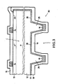
- FIG. 1 shows the embodiment of a solar cell (19) constructed according to the invention, which consists of a p-doped silicon substrate as the body (1), a thin silicon oxide layer (2), ohmic contacts (4) and an MIS (metal) Insulator semiconductor) contact, which in turn consists of the p-silicon of the silicon body (1), the silicon oxide layer (2) and a metallization (3) preferably made of aluminum or magnesium or a double layer of Mg / Al put together.
- the ohmic contacts (4) are arranged discontinuously on the semiconductor substrate (1), these being arranged according to the invention on the free end faces (31) of elevations (21).
- the ohmic contacts (4), together with the elevated silicon regions (21) underneath, can form a geometry that can be described by interconnected strips, rings or dots.
- Passivation layers extend between the elevated ohmic contact areas (4), which are composed on the one hand of the natural or below 800 ° C silicon oxide layer (2) and a further insulator layer (5), both for passivation and as an anti-reflection layer can serve.
- the thickness of the upper passivation layer (5), referred to as the first, can be approximately 80 nm and preferably consists of aluminum oxide or silicon nitride.
- the further insulator layer, which is referred to as the second passivation layer, in the form of the silicon oxide layer (2) can be constructed differently on the front and back of the silicon substrate (1). The thickness on the front can be varied within wide limits since it does not act as a tunnel insulator. However, it can also be completely omitted there.
- a natural silicon oxide layer is understood to be that which is always present on the silicon substrate (1) and is only a few atomic layers thick.
- the structure of the silicon oxide layer (2) itself can be changed on the front side by the subsequent deposition of the first passivation layer (5), for example silicon nitride.
- silicon oxide can be converted into silicon oxynitride.
- the charge carriers generated mainly by the light near the front first have to diffuse through the entire substrate (1) in order to be collected by the MIS contact on the back. It is extremely important that the front side, which is composed of the area of the ohmic contacts (4) and the silicon surface covered by the passivation layers (2) and (5), has a low surface recombination speed, since otherwise a large part of the Charge carriers would already recombine there.
- the ohmic contacts (4) are lifted out of the surface by a silicon etching process and, depending on the height of the regions, their influence on recombination is more or less eliminated.
- This measure namely increases the distance between the ohmic contacts (4) both from the point of generation of the charge carriers in the silicon volume (1) and from the collecting MIS contact (3), so that the minority charge carriers prefer to the MIS because of the now higher concentration gradient - Diffuse contact and be used there.
- the distance between the ohmic contacts (4) (surface (31)) and the opposite MIS contact (3) (surface (27)) should advantageously be greater than the diffusion length of the minority charge carriers.
- the thickness of the silicon substrate (1) in the region (22) can be greater, equal or smaller, but preferably considerably smaller than the diffusion length. If, however, the thickness is considerably smaller than the diffusion length, as many of the minority charge carriers that are formed on the surface can diffuse to the rear, without recombining.
- This optimization of the substrate thickness and the height of the ohmic contact areas can take place independently of one another by means of the arrangement according to the invention, by suitable choice of the starting layer thickness of the silicon and by the duration of the etching process.
- Another advantage is that the raised silicon webs (21) under the ohmic contact (4) serve as mechanical reinforcement for the silicon volume (1).
- the ohmic contacts (4) are preferably arranged in the shape of a finger, i. that is, they are composed of webs that run parallel to one another and are connected to one another on one side (comb shape).
- the distance between the ohmic contact fingers should be much greater than the thickness d (distance between surfaces (22) and (27)) of the silicon substrate (1) or as the diffusion length of the minority charge carriers, so that on average the way to collect them MIS contact is less than to the ohmic contact area.
- the distance between the ohmic contacts (4) is limited by the series resistance.
- the optimal distance is in the range of 1 to 5 mm, the finger width in the range of 50 to 300 ⁇ m, which means that a proportion of contact area or shading of less than 10% can be achieved.
- the rear metal (3) of the MIS contact serves as a reflector for the light not absorbed, so that the light path in the silicon and thus the generation of charge carriers is essential is increased, which in particular enables the advantageous use of very thin, cheap solar silicon.
- the reflection of the infrared portion of the sunlight on the back leads to less heating of the solar cell and thus to a higher efficiency under real operating conditions.
- FIG. 2 and 3 show further configurations of solar cells (20) and (30) which obey the teaching according to the invention.
- the respective ohmic contact (10) or (16) is arranged on the back of the solar cell (20) or (30), specifically directly on the semiconductor substrate body (6) or (21) and also in regions, such as it was already the case in FIG. 1.
- the solar cell (20) shown in FIG. 2 corresponds to the basic structure according to the silicon nitride inversion layer solar cell described in DE-PS 28 40 096 with MIS contacts.
- the solar cell (20) has a p-silicon substrate or body (6) on which a thin silicon oxide layer (7) is arranged.
- MIS contacts are arranged on the front, which are composed of the semiconductor substrate (6), the silicon oxide layer (7) and discontinuously of metal layers (8) which are preferably arranged in strip form.
- the electrons (minority charge carriers) generated by the light diffuse to the front and are accelerated there in the electrical field generated by the positive insulator charges and migrate along the highly conductive inversion layer to the MIS contacts, through which they leave the silicon body (6) and reach an external circuit.
- a further passivation layer (11) is also provided, which also covers the ohmic contacts (10).
- the decisive training is then to be found that the ohmic contacts (10) are raised, i.e. on protrusions (23) which rise from the normal surface (24) and are formed by a silicon etching process.
- the influence of the ohmic contacts (10) on the recombination of the charge carriers is greatly reduced or is completely eliminated at distances from the point of origin which are considerably greater than the diffusion length.
- the actual silicon substrate (6) can thus be made thinner without increasing the recombination. As a result, both the efficiency in terms of the light coming in from the front and the light coming in from the rear is significantly increased.
- the decisive advantage also applies here that the mechanical stability of the thin silicon substrate (6) is significantly improved by the silicon elevations or struts (23) below the ohmic contact (10) and thus the economical production of highly efficient extremely thin (d ⁇ 50 ⁇ m) ) silicon solar cells that can be illuminated on both sides is only possible. It should be noted in particular that this takes place without any significant additional technological effort.
- Silicon nitride or silicon oxynitride (produced in plasma) or aluminum oxide or aluminum oxynitride are preferably suitable for passivating the rear side by means of the transparent passivation or insulator layer (11).
- the production temperatures are between 300 ° C and 600 ° C.
- the function of these layers on the back is completely different from that on the front. In the latter case, high positive charges must be present at the interface so that a highly conductive inversion layer (electron gas) is generated just below the surface.
- the surface recombination speed must be greatly reduced; a highly conductive inversion layer is rather harmful here, since it leads the minority charge carriers to the ohmic contacts, where they recombine and are therefore lost from use.
- the rear silicon nitride layer (11) is produced at higher temperatures compared to the nitride layer (9) on the front.
- the surface recombination is thus reduced. This means that the inversion layer that arises due to the high charge densities or that is greatly increased in its conductivity is accepted.
- the present invention with the ohmic contacts (10) reset by etching also considerably reduces the disadvantageous influence of the inversion layer, in that constant distance between the ohmic contacts, the length of the inversion layer and thus its resistance is considerably increased, and the flow of the minority charge carriers to the ohmic contacts is severely restricted.
- the recombination can be reduced further by means of higher insulator charge densities, without having to accept the additional disadvantage with regard to the inversion layer.
- This advantage also applies to the solar cell shown in FIG. 1 with the raised ohmic contact grid on the front.
- Aluminum oxide as the insulator layer (11) contains negative charges, which lead to an accumulation of holes on the silicon surface on p-silicon.
- the problem with the inversion layer advantageously does not occur there, the electrons as minority charge carriers are repelled by the potential barrier from the rear.
- a highly reflective metal e.g. Al, Ag
- the transparent insulator layer (11) over the entire back, for example by vacuum evaporation or sputtering.
- a highly reflective metal e.g. Al, Ag
- the path of the light incident from the front in the silicon is doubled by reflection and the efficiency is increased, in particular for thin, cheap solar silicon.
- FIG. 3 shows a solar cell (30) which obeys the teaching according to the invention and which can be a conventional n+p or p+n solar cell.
- the n+p solar cell (30) shown in the exemplary embodiment comprises a semiconductor substrate (12), a highly doped surface layer (13) (here n+), on the front side an ohmic contact (14) in the form of a lattice and not arranged flat a front anti-reflective layer (15).
- On the back side there are also ohmic contacts (16) and passivation layers which are arranged in a non-planar manner, preferably in the form of a web or grid, preferably in the form of a silicon oxide layer (17) and an insulating layer (18) which also acts as an antireflection layer.
- the insulating layer (18) is preferably formed from aluminum oxide or silicon nitride.
- the ohmic contacts (16) are now preferably arranged in the form of fingers on elevations (25) which are lifted out of the surface (26) by silicon etching.
- the ohmic contacts (16) are clearly covered by the passivation layer (18).
- the inventive design of the solar cell (30) achieves the same advantages as the solar cell (20) according to FIG. 2.
- a difference between the two cells (20) and (30) lies in the fact that the solar cell (30) with pn- Transition contained high temperature processes, while the entire solar cell (20) is manufactured by simple low temperature processes.
- Both solar cells can take advantage of both the solar radiation hitting the front and the rear.
- a reflective metal can be applied to the back.
Abstract
Es wird eine Siliziumsolarzelle (19) mit einem Substratkörper (1) vorgeschlagen, auf dessen einer Seite ein elektrisches Feld durch einen MIS-Kontakt (1, 2, 3) erzeugt wird, um eine Trennung von durch Strahlungsenergie erzeugten Ladungsträger hervorzurufen. Die Minoritätsladungsträger werden im Metall (3) des MIS-Kontakt abgesaugt, wohingegen die Majoritätsladungsträger über auf der gegenüberliegenden Seite angeordnete Ohm'sche Kontakte (4) abgeleitet werden. Die Ohm'schen Kontakte (4) befinden sich auf gegenüber der Substratoberfläche (22) erhabenen Bereiche (21). Ferner ist die die Ohm'schen Kontakte (4) aufweisende Seite des Substratkörpers (1) mit zumindest einer Passivierungsschicht (5) vollständig abgedeckt.A silicon solar cell (19) with a substrate body (1) is proposed, on one side of which an electric field is generated by an MIS contact (1, 2, 3) in order to cause a separation of charge carriers generated by radiation energy. The minority charge carriers are sucked off in the metal (3) of the MIS contact, whereas the majority charge carriers are discharged via ohmic contacts (4) arranged on the opposite side. The ohmic contacts (4) are located on regions (21) which are raised in relation to the substrate surface (22). Furthermore, the side of the substrate body (1) having the ohmic contacts (4) is completely covered with at least one passivation layer (5).
Description
Die Erfindung bezieht sich auf eine Solarzelle, insbesondere Dünnschicht-Solarzelle aus einem Halbleitermaterial wie Silizium, in deren Halbleitersubstrat durch Strahlungsenergie Minoritäts- und Majoritäts-Ladungsträger erzeugt werden, die durch ein elektrisches Feld trennbar und sodann ableitbar sind, wobei auf einer (ersten) Halbleitersubstratfläche zueinander beabstandete Ohm'sche Kontakte angeordnet sind, die untereinander verbunden sind, und wobei zumindest zwischen den Ohm'schen Kontakten eine Passivierungsschicht angeordnet ist, die vorzugsweise auch die Ohm'schen Kontakte mit abdeckt. Ferner bezieht sich die Erfindung auch auf ein Verfahren zur Herstellung einer Solarzelle.The invention relates to a solar cell, in particular thin-film solar cell made of a semiconductor material such as silicon, in the semiconductor substrate of which minority and majority charge carriers are generated by radiation energy, which are separable by an electric field and then derivable, with a (first) semiconductor substrate surface mutually spaced ohmic contacts are arranged, which are interconnected, and at least between the ohmic contacts a passivation layer is arranged, which preferably also covers the ohmic contacts. Furthermore, the invention also relates to a method for producing a solar cell.
Bei einem Aufbau einer entsprechenden Solarzelle kann die Rekombination von Ladungsträgern im Bereich der Ohm'schen Kontakte reduziert werden, ohne daß eine Potentialschwelle für Minoritätsladungsträger durch Legieren, Diffusion oder Ionenimplantation im Halbleitersubstrat erzeugt werden muß.If a corresponding solar cell is constructed, the recombination of charge carriers in the region of the ohmic contacts can be reduced without a potential threshold for minority charge carriers having to be generated in the semiconductor substrate by alloying, diffusion or ion implantation.
Aufgabe der vorliegenden Erfindung ist es daher, eine Solarzelle der eingangs beschriebenen Art so auszubilden, daß die Dicke des Halbleitersubstrats erheblich reduziert werden kann, ohne daß die Gefahr einer erhöhten Rekombination im Bereich der Ohm'schen Kontakte erwächst. Vielmehr soll trotz Reduzierung der Halbleitermaterialdicke die Rekombination im Bereich der Ohm'schen Kontakte weitergehend verringert werden, wobei das Fernhalten von Ladungsträgern von den Ohm'schen Kontakten nicht notwendigerweise durch eine Potentialbarriere erfolgen muß.The object of the present invention is therefore to design a solar cell of the type described in the introduction in such a way that the thickness of the semiconductor substrate can be reduced considerably without that the risk of increased recombination in the area of ohmic contacts increases. Rather, despite the reduction in the semiconductor material thickness, the recombination in the area of the ohmic contacts is to be reduced further, the charge carriers not necessarily having to be kept away from the ohmic contacts by a potential barrier.
Die Aufgabe wird erfindungsgemäß dadurch gelöst, daß das die Minoritäts- und Majoritätsladungsträger trennende elektrische Feld im Bereich einer (zweiten) Substratkörperfläche verläuft, die der die Ohm'schen Kontaktbereiche aufweisenden ersten Substratkörperfläche gegenüberliegt, so daß die Majoritätsladungsträger zu den Ohm'schen Kontaktbereichen diffundieren und von diesen gesammelt werden und daß die Ohm'schen Kontakte auf ersten Bereichen der ersten Halbleitersubstratfläche angeordnet sind, die gegenüber zwischen den Ohm'schen Kontakten vorhandenen zweiten Bereichen des Halbleitersubstrats erhaben sind.The object is achieved in that the electric field separating the minority and majority charge carriers extends in the region of a (second) substrate body surface which is opposite the first substrate body surface having the ohmic contact regions, so that the majority charge carriers diffuse to the ohmic contact regions and of these are collected and that the ohmic contacts are arranged on first regions of the first semiconductor substrate surface which are raised opposite second regions of the semiconductor substrate which are present between the ohmic contacts.
Bei der erfindungsgemäßen Lehre dienen die Ohm'schen Kontakte zur Sammlung der Majoritätsladungsträger und sind direkt auf dem Substratmaterial ohne eine dotierte Zwischenschicht (d.h. ohne spezielle Abschirmung durch eine Potentialbarriere) angebracht. Aufgrund des Fehlens der Potentialbarriere könnten neben den Majoritätsladungsträgern grundsätzlich auch Minoritätsladungsträger zu den Ohm'schen Kontakten gelangen, gleichwenn letztere bei idealem Verhalten zum trennenden elektrischen Feld auf der den Ohm'schen Kontakten gegenüberliegenden Seite diffundieren sollten. Um jedoch eine Rekombination von Majoritäts- und Minoritätsladungsträgern im Bereich der Ohm'schen Konktakte zu reduzieren, wird erfindungsgemäß vorgeschlagen, daß die Ohm'schen Kontakte z.B. als schmale Streifen erhöht gegenüber ihrer sehr gut mit einer Isolatorschicht passivierten Umgebung angebracht werden. Hierdurch wird erreicht, daß auch bei sehr dünnen Halbleitersubstraten die Entfernung der Ohm'schen Kontakte von der gegenüberliegenden Minoritätsträger sammelnden Seite relativ groß, vorzugsweise größer als die Diffusionslänge der Minoritätsladungsträger wird, so daß nur wenige Minoritätsladungsträger zu den Ohm'schen Kontakten gelangen können (geringer Konzentrationsgradient in Richtung der Ohm'schen Kontakte). Hierin sind die wesentlichen Unterschiede zum Stand der Technik zu erkennen, auch wenn es bereits bekannt ist, Ohm'sche Kontakte erhaben auszubilden, wie es z.B. in den US-A-4,322,571, US-A-4,367,368 oder die US-A-4,135,950 der Fall ist. Bei den dort beschriebenen Solarzellen sind jedoch die Ohm'schen Kontakte durch eine Potentialbarriere abgeschirmt. Die Ohm'schen Kontakte sind nicht unmittelbar auf das Halbleitersubstrat aufgebracht. Außerdem befindet sich zwischen den Ohm'schen Kontakten keine Passivierungsschicht. Schließlich haben die Ohm'schen Kontakte nach dem Stand der Technik nicht die Aufgabe, die Stabilität von Dünnschicht-Solarzellen zu verbessern, also Zellen, die eine Substratstärke aufweisen, die so dünn ist, daß die Gefahr eines Zerbrechens bestünde.In the teaching according to the invention, the ohmic contacts serve to collect the majority charge carriers and are attached directly to the substrate material without a doped intermediate layer (ie without special shielding by means of a potential barrier). Due to the lack of the potential barrier, in addition to the majority charge carriers, minority charge carriers could in principle also reach the ohmic contacts, even if the latter should diffuse with ideal behavior to the separating electrical field on the side opposite the ohmic contacts. However, in order to reduce a recombination of majority and minority charge carriers in the area of the ohmic contacts, it is proposed according to the invention that the ohmic contacts are applied, for example as narrow strips, in an elevated manner compared to their surroundings, which are very well passivated with an insulator layer. Through this What is achieved is that even with very thin semiconductor substrates the distance of the ohmic contacts from the opposite minority carrier collecting side becomes relatively large, preferably greater than the diffusion length of the minority charge carriers, so that only a few minority charge carriers can reach the ohmic contacts (low concentration gradient towards the ohmic contacts). This shows the essential differences from the prior art, even if it is already known to form ohmic contacts in a raised manner, as described, for example, in US Pat. Nos. 4,322,571, 4,367,368 or 4,135,950 Case is. In the solar cells described there, however, the ohmic contacts are shielded by a potential barrier. The ohmic contacts are not applied directly to the semiconductor substrate. In addition, there is no passivation layer between the ohmic contacts. Finally, the ohmic contacts according to the prior art do not have the task of improving the stability of thin-film solar cells, that is to say cells which have a substrate thickness which is so thin that there is a risk of breakage.
Mit anderen Worten wird erfindungsgemäß vorgeschlagen, daß die Ohm'schen Kontakte von der durch die Passivierungsschicht (Isolatorschicht) sehr gut passivierten sonstigen Halbleiteroberfläche räumlich getrennt werden. Hierdurch kann außerhalb der Ohm'schen Kontakte eine Halbleitersubstratdicke, die kleiner als die Diffusionslänge der Minoritätsladungsträger ist, gewählt werden, so daß ein hoher Wirkungsgrad der Solarzelle erzielbar ist. Allerdings wird nicht die Rekombination im Bereich der Ohm'schen Kontakte erhöht, da in diesem Bereich der Abstand zu der gegenüberliegenden Seite des Halbleitersubstrats vorzugsweise erheblich größer als die Diffusionslänge der Minoritätsladungsträger ist.In other words, it is proposed according to the invention that the ohmic contacts are spatially separated from the other semiconductor surface, which is very well passivated by the passivation layer (insulator layer). As a result, a semiconductor substrate thickness that is smaller than the diffusion length of the minority charge carriers can be selected outside the ohmic contacts, so that a high efficiency of the solar cell can be achieved. However, the recombination is not increased in the area of the ohmic contacts, since in this area the distance to the opposite side of the semiconductor substrate is preferably considerably greater than the diffusion length of the minority charge carriers.
Die Strukturierung der die Ohm'schen Kontakte aufweisenden Halbleiteroberfläche erfolgt vorzugsweise durch selektives Ätzen. Dabei geht man von einer entsprechend dicken Halbleiterscheibe aus, die vorzugsweise stärker als die Diffusionslänge der Minoritätsladungsträger ist. Anschließend bestimmt man die Ohm'schen Kontaktbereiche, um diese durch eine geeignete Ätzmaske abzudecken. Anschließend werden die nicht abgedeckten Bereiche bis zu der gewünschten Dicke des Halbleitersubstrats weggeätzt. Sofern die Ätzmaske nicht gleichzeitig durch das Metall der Ohm'schen Kontakte gebildet wird -hierin ist ein weiteres erfindungsgemäßes Merkmal zu sehen-, wird nach dem Ätzen die Ätzmaske entfernt, um gegebenenfalls das Metall des Ohm'schen Kontaktes aufzubringen. Als Ätzmaske kann z.B. Photolack, SiO₂ oder Si₃N₄ benutzt werden. Es besteht auch die Möglichkeit, daß sich das Metall unter der Ätzmaske befindet.The semiconductor surface having the ohmic contacts is preferably structured by selective etching. This is based on a correspondingly thick semiconductor wafer, which is preferably stronger than the diffusion length of the minority charge carriers. The ohmic contact areas are then determined in order to cover them with a suitable etching mask. The uncovered areas are then etched away to the desired thickness of the semiconductor substrate. If the etching mask is not simultaneously formed by the metal of the ohmic contacts — a further feature according to the invention can be seen here — the etching mask is removed after the etching in order to apply the metal of the ohmic contact if necessary. As an etching mask, e.g. Photoresist, SiO₂ or Si₃N₄ can be used. There is also the possibility that the metal is under the etching mask.
Bei dem Ätzen selbst kann es sich um isotropes oder anisotropes Ätzen handeln, um chemisches Ätzen oder Plasma-, Ionen-, reaktives Ionen- oder Laserätzen. Besonders vorteilhaft ist die Verwendung des anisotropen Ätzens nämlich dann, wenn man ein (100) orientiertes Silizium benutzt, da bekanntlich die (100) Oberfäche wesentlich schneller geätzt wird als die (111) Fläche. In diesem Falle befinden sich unter der Ätzmaske im Schnitt trapezförmig ausgebildete Bereiche, deren Kantenwinkel 54,7° beträgt. Auf die Spitzen, also die äußeren Stirnflächen dieser Bereiche werden dann die Ohm'schen Kontakte aufgebracht. Als anisotrope Ätzmittel kommen insbesondere die bekannten Strukturätzen auf der Basis von z.B. Kaliumhydroxid oder Äthylendiamin in Frage. Auch (110) Oberflächen können vorteilhafterweise in Verbindung mit dem anisotropen Ätzen verwendet werden, wobei durch senkrechte Wände begrenzte erhabene Bereiche enstehen. Im Schnitt ergibt sich eine Rechteckform.The etching itself can be isotropic or anisotropic, chemical etching or plasma, ion, reactive ion or laser etching. The use of anisotropic etching is particularly advantageous when using (100) oriented silicon, since it is known that the (100) surface is etched much faster than the (111) surface. In this case, there are trapezoidal sections under the etching mask, the edge angle of which is 54.7 °. The ohmic contacts are then applied to the tips, that is to say the outer end faces of these regions. The known structure etches based on, for example, potassium hydroxide or ethylenediamine are particularly suitable as anisotropic etchants. (110) Surfaces can also advantageously be used in connection with the anisotropic etching, with raised areas delimited by vertical walls. The cut is rectangular.
Erwähntermaßen dienen nach einem eigenerfinderischen Vorschlag die Ohm'schen Kontakte gleichzeitig als Ätzmaske. Zusammen mit dem Ätzvorgang erfolgt gleichzeitig eine Texturierung der nicht abgedeckten Bereiche zur Erhöhung des Lichteinfalles der mit der Isolatorschicht passivierten Si-Oberfläche.According to a suggestion made by the inventor, the ohmic contacts also serve as an etching mask. Together with the etching process, the uncovered areas are textured at the same time in order to increase the incidence of light of the Si surface passivated with the insulator layer.
Zu den Metallen der Ohm'schen Kontakte selbst ist zu bemerken, daß diese z.B. durch Vakuumaufdampfen durch eine mechanische Maske, durch Siebdruck, durch Kathodenzerstäubung aufgebracht und gegebenenfalls mit Photolithograpie strukturiert werden können.Regarding the metals of the ohmic contacts themselves, it should be noted that these e.g. can be applied by vacuum evaporation through a mechanical mask, by screen printing, by sputtering and, if necessary, structured with photolithography.
Durch die für die Ohm'schen Kontakte bestimmten erhabenen Bereiche ergibt sich ferner der Vorteil, daß das Halbleitersubstrat stabiler wird, gleichwenn zwischen den Erhebungen die Schichtdicke überaus gering ist, ohne daß die Gefahr einer Bruchanfälligkeit erwächst. Dies spielt insbesondere bei der Verwendung von billigerem ein- und polykristallinem ("solar-grade") Siliziummaterial eine große Rolle, das eine geringere Diffusionslänge für die Minoritätsladungsträger besitzt.The raised areas intended for the ohmic contacts also have the advantage that the semiconductor substrate becomes more stable, even if the layer thickness between the elevations is extremely small, without the risk of susceptibility to breakage. This is particularly important when using cheaper single-crystal and polycrystalline ("solar-grade") silicon material, which has a shorter diffusion length for the minority charge carriers.
Dadurch kann u.a. auch bei diesem Material die von hinten auf die Solarzelle auftreffende Strahlung ausgenützt werden.This means that With this material, too, the radiation striking the solar cell from behind is used.
Ein weiterer Vorteil der erfindungsgemäßen Ausbildung der Solarzelle besteht darin, daß die Kontaktierung dünner Solarzellen beispielsweise durch Ultraschallschweißen wesentlich erleichtert wird, in dem diese auf den durch die Ohm'schen Kontakte bedeckten dicken Halbleiterbereich bzw. auf einem zusätzlich, aber gleichzeitig mit der Ätzung der Ohm'schen Kontaktbereiche am Rand erzeugten Kontaktierbereich aus dickem Halbleitermaterial ohne Gefahr des Bruches der dünnen Siliziumbereiche erfolgt. Weiterhin erlaubt es diese Anordnung mit einer über den Rand der Solarzelle sich erstreckenden Passivierungsschicht, daß der Vorderseitenkontakt über den Rand zur Rückseite geführt und dort kontaktiert wird. Beide Anschlüsse auf einer Seite zu kontaktieren -z.B. mit Ultraschallvereinfacht wesentlich den Herstellungsprozeß.Another advantage of the design of the solar cell according to the invention is that the contacting of thin solar cells is made considerably easier, for example by ultrasonic welding, in that this is done on the thick semiconductor region covered by the ohmic contacts or on an additional but simultaneously with the etching of the ohms 'Contact areas generated at the edge made of thick semiconductor material without risk of breaking the thin silicon areas. Furthermore, this arrangement with a passivation layer extending over the edge of the solar cell allows the front-side contact to pass over the edge led to the back and contacted there. Contacting both connections on one side - e.g. using ultrasound - significantly simplifies the manufacturing process.
Der erfindungsgemäß vorgeschlagene Aufbau der Solarzelle kann für ein- und polykristallines Silizium sowie für Verbindungshalbleiter Verwendung finden.The structure of the solar cell proposed according to the invention can be used for single and polycrystalline silicon and for compound semiconductors.
Ausgestaltungen der Erfindung ergeben sich aus den Ansprüchen und den diesen zu entnehmenden Merkmalen -für sich und/oder in Kombination-.Embodiments of the invention result from the claims and the features to be extracted from them - individually and / or in combination.
Weitere Einzelheiten, Vorteile und Merkmale der Erfindung sind der nachfolgenden Beschreibung von in einer Zeichnung dargestellten bevorzugten Ausführungsformen zu entnehmen.Further details, advantages and features of the invention can be found in the following description of preferred embodiments shown in a drawing.
Es zeigen:
- Fig. 1 eine erste Ausführungsform einer erfindungsgemäßen Siliziumsolarzelle mit frontseitigen Ohm'schen Kontakten,
- Fig. 2 eine Siliziumsolarzelle mit rückseitigen Ohm'schen Kontakten und
- Fig. 3 eine weitere Ausführungsform einer Siliziumsolarzelle mit rückseitigen Ohm'schen Kontakten.
- 1 shows a first embodiment of a silicon solar cell according to the invention with ohmic contacts on the front,
- Fig. 2 is a silicon solar cell with Ohm rear contacts and
- 3 shows a further embodiment of a silicon solar cell with ohmic contacts on the rear.
In Fig. 1 ist die Ausführungsform einer erfindungsgemäß aufgebauten Solarzelle (19) dargestellt, die aus einem p-dotierten Siliziumsubstrat als Körper (1), einer dünnen Siliziumoxidschicht (2), Ohm'schen Kontakten (4) sowie einem MIS- (Metal-Insulator-Semiconductor) Kontakt besteht, der sich seinerseits aus dem p-Silizium des Siliziumkörpers (1), der Siliziumoxidschicht (2) und einer Metallisierung (3) vorzugsweise aus Aluminium oder Magnesium oder einer Doppelschicht Mg/Al zusammensetzt. Die Ohm'schen Kontakte (4) sind diskontinuierlich auf dem Halbleitersubstrat (1) angeordnet, wobei diese erfindungsgemäß auf den freien Stirnflächen (31) von Erhebungen (21) angeordnet sind. Hierdurch wird erreicht, daß der Abstand zwischen den Ohm'schen Kontakten und der gegenüberliegenden Seite (27) des Halbleitersubstrats (1) größer als im übrigen Oberflächenbereich des Halbleitersubstrats (1) ist. Dabei ist dieser Bereich mit dem Bezugszeichen (22) versehen. Die Ohm'schen Kontakte (4) können zusammen mit den darunterliegenden erhöhten Siliziumbereichen (21) eine Geometrie bilden, die durch miteinander verbundene Streifen, Ringe oder Punkte zu beschreiben sind.1 shows the embodiment of a solar cell (19) constructed according to the invention, which consists of a p-doped silicon substrate as the body (1), a thin silicon oxide layer (2), ohmic contacts (4) and an MIS (metal) Insulator semiconductor) contact, which in turn consists of the p-silicon of the silicon body (1), the silicon oxide layer (2) and a metallization (3) preferably made of aluminum or magnesium or a double layer of Mg / Al put together. The ohmic contacts (4) are arranged discontinuously on the semiconductor substrate (1), these being arranged according to the invention on the free end faces (31) of elevations (21). This ensures that the distance between the ohmic contacts and the opposite side (27) of the semiconductor substrate (1) is greater than in the remaining surface area of the semiconductor substrate (1). This area is provided with the reference symbol (22). The ohmic contacts (4), together with the elevated silicon regions (21) underneath, can form a geometry that can be described by interconnected strips, rings or dots.
Zwischen den erhöhten Ohm'schen Kontaktbereichen (4) erstrecken sich Passivierungsschichten, die sich zum einen aus der natürlichen oder auch unterhalb von 800°C erzeugten Siliziumoxidschicht (2) und einer weiteren Isolatorschicht (5) zusammensetzen, die sowohl zur Passivierung wie auch als Antireflektionsschicht dienen kann. Die Dicke der oberen, als erste bezeichnete Passivierungsschicht (5) kann dabei ungefähr 80 nm betragen und besteht vorzugsweise aus Aluminiumoxid oder Siliziumnitrid. Die weitere Isolatorschicht, die als zweite Passivierungsschicht bezeichnet wird, in Form der Siliziumoxidschicht (2) kann auf der Vorder- und Rückseite des Siliziumsubstrats (1) unterschiedlich aufgebaut sein. So kann auf der Vorderseite die Dicke in weiteren Grenzen variiert werden, da sie nicht als Tunnelisolator wirkt. Sie kann dort aber auch vollständig entfallen.Passivation layers extend between the elevated ohmic contact areas (4), which are composed on the one hand of the natural or below 800 ° C silicon oxide layer (2) and a further insulator layer (5), both for passivation and as an anti-reflection layer can serve. The thickness of the upper passivation layer (5), referred to as the first, can be approximately 80 nm and preferably consists of aluminum oxide or silicon nitride. The further insulator layer, which is referred to as the second passivation layer, in the form of the silicon oxide layer (2) can be constructed differently on the front and back of the silicon substrate (1). The thickness on the front can be varied within wide limits since it does not act as a tunnel insulator. However, it can also be completely omitted there.
Für die Grenzflächenpassivierung kann sowohl die natürliche Siliziumoxidschicht als auch eine beispielsweise durch thermische oder anders geartete Oxidation speziell präparierte Siliziumoxidschicht (2) verwendet werden. Unter natürlicher Siliziumoxidschicht versteht man diejenige, die stets auf dem Siliziumsubstrat (1) vorhanden ist und nur wenige Atomlagen dick ist. Die Siliziumoxidschicht (2) selbst kann auf der Vorderseite durch die nachfolgende Abscheidung der ersten Passivierungsschicht (5) -z.B. Siliziumnitrid- in ihrer Strukturzusammensetzung verändert werden. So kann z.B. eine Umwandlung von Siliziumoxid in Siliziumoxynitrid erfolgen.Both the natural silicon oxide layer and a silicon oxide layer (2) specially prepared, for example, by thermal or other types of oxidation, can be used for the interface passivation. A natural silicon oxide layer is understood to be that which is always present on the silicon substrate (1) and is only a few atomic layers thick. The structure of the silicon oxide layer (2) itself can be changed on the front side by the subsequent deposition of the first passivation layer (5), for example silicon nitride. For example, silicon oxide can be converted into silicon oxynitride.
Anders als bei konventionellen Solarzellen müssen die in der Hauptsache nahe der Frontseite durch das Licht erzeugten Ladungsträger erst durch das ganze Substrat (1) diffundieren, um vom rückseitigen MIS-Kontakt gesammelt zu werden. Dabei ist es äußerst wichtig, daß die Vorderseite, die sich aus dem Bereich der Ohm'schen Kontakte (4) und der durch die Passivierungsschichten (2) und (5) bedeckten Siliziumoberfläche zusammensetzt, eine niedrige Oberflächenrekombinationsgeschwindigkeit besitzt, da andernfalls ein großer Teil der Ladungsträger dort schon rekombinieren würde.In contrast to conventional solar cells, the charge carriers generated mainly by the light near the front first have to diffuse through the entire substrate (1) in order to be collected by the MIS contact on the back. It is extremely important that the front side, which is composed of the area of the ohmic contacts (4) and the silicon surface covered by the passivation layers (2) and (5), has a low surface recombination speed, since otherwise a large part of the Charge carriers would already recombine there.
Erfindungsgemäß werden durch einen Silizium-Ätzprozeß die Ohm'schen Kontakte (4) aus der Oberfläche herausgehoben und damit, je nach Höhe der Bereiche, ihr Rekombinationseinfluß mehr oder weniger eliminiert. Durch diese Maßnahme wird nämlich der Abstand der Ohm'schen Kontakte (4) sowohl vom Erzeugungsort der Ladungsträger im Siliziumvolumen (1) wie auch vom sammelnden MIS-Kontakt (3) erheblich vergrößert, so daß die Minoritätsladungsträger wegen des jetzt höheren Konzentrationsgradienten bevorzugt zum MIS-Kontakt diffundieren und dort genutzt werden. Vorteilhafterweise sollte der Abstand der Ohm'schen Kontakte (4) (Fläche (31)) vom gegenüberliegenden MIS-Kontakt (3) (Fläche (27)) größer als die Diffusionslänge der Minoritätsladungsträger sein. Die Dicke des Siliziumsubstrats (1) im Bereich (22) kann größer, gleich oder kleiner, vorzugsweise jedoch erheblich kleiner als die Diffusionslänge sein. Sofern jedoch die Dicke erheblich kleiner als die Diffusionslänge ist, können möglichst viele der an der Oberfläche entstehenden Minoritätsladungsträger zur Rückseite diffundieren, ohne zu rekombinieren. Diese Optimierung von Substratdicke und Höhe der Ohm'schen Kontaktbereiche kann durch die erfindungsgemäße Anordnung unabhängig voneinander durch geeignete Wahl der Ausgangsschichtdicke des Siliziums und durch die Dauer des Ätzprozesses erfolgen. Als weiterer Vorteil ergibt sich, daß die erhabenen Siliziumstege (21) unter dem Ohm'schen Kontakt (4) quasi als mechanische Verstärkung für das Siliziumvolumen (1) dienen. Dieses muß, um insbesondere für billiges Solarsilizium (geringe Diffusionslänge) hohe Wirkungsgrade zu gewährleisten, möglichst dünn sein (bis herab zu 10 µm), was ohne die mechanisch stabileren Ohm'schen Kontaktbereiche nicht zu realisieren ist -zumindest nicht auf größeren Flächen. Dadurch wird die Herstellung von Solarzellen auf dünnstem Silizium auch großtechnisch ermöglicht. Weiterhin kann gleichzeitig mit dem Ätzen (anisotropes Ätzen) die Texturierung der Siliziumoberfläche zur Erhöhung des Lichteinfalls erfolgen.According to the invention, the ohmic contacts (4) are lifted out of the surface by a silicon etching process and, depending on the height of the regions, their influence on recombination is more or less eliminated. This measure namely increases the distance between the ohmic contacts (4) both from the point of generation of the charge carriers in the silicon volume (1) and from the collecting MIS contact (3), so that the minority charge carriers prefer to the MIS because of the now higher concentration gradient - Diffuse contact and be used there. The distance between the ohmic contacts (4) (surface (31)) and the opposite MIS contact (3) (surface (27)) should advantageously be greater than the diffusion length of the minority charge carriers. The thickness of the silicon substrate (1) in the region (22) can be greater, equal or smaller, but preferably considerably smaller than the diffusion length. If, however, the thickness is considerably smaller than the diffusion length, as many of the minority charge carriers that are formed on the surface can diffuse to the rear, without recombining. This optimization of the substrate thickness and the height of the ohmic contact areas can take place independently of one another by means of the arrangement according to the invention, by suitable choice of the starting layer thickness of the silicon and by the duration of the etching process. Another advantage is that the raised silicon webs (21) under the ohmic contact (4) serve as mechanical reinforcement for the silicon volume (1). In order to ensure high efficiencies, especially for cheap solar silicon (short diffusion length), this must be as thin as possible (down to 10 µm), which cannot be achieved without the mechanically more stable ohmic contact areas - at least not on larger areas. This enables the manufacture of solar cells on the thinnest silicon on an industrial scale. Furthermore, the texturing of the silicon surface to increase the incidence of light can take place simultaneously with the etching (anisotropic etching).
Die Ohm'schen Kontakte (4) sind vorzugsweise in Fingerform angeordnet, d. h., sie setzen sich aus parallel zueinander verlaufenden Stegen zusammen, die an einer Seite miteinander verbunden sind (Kammform). Dabei soll der Abstand der Ohm'schen Kontaktfinger untereinander wesentlich größer sein als die Dicke d (Abstand zwischen Flächen (22) und (27)) des Siliziumsubstrats (1) bzw. als die Diffusionslänge der Minoritätsladungsträger, so daß im Mittel der Weg zum sammelnden MIS-Kontakt geringer ist als zu dem Ohm'schen Kontaktbereich. Nach oben ist der Abstand der Ohm'schen Kontakte (4) durch den Serienwiderstand begrenzt. Der optimale Abstand liegt im Bereich von 1 bis 5 mm, die Fingerbreite im Bereich von 50 bis 300 µm, wodurch sich ein Kontaktflächenanteil bzw. eine Abschattung von weniger als 10% erreichen läßt.The ohmic contacts (4) are preferably arranged in the shape of a finger, i. that is, they are composed of webs that run parallel to one another and are connected to one another on one side (comb shape). The distance between the ohmic contact fingers should be much greater than the thickness d (distance between surfaces (22) and (27)) of the silicon substrate (1) or as the diffusion length of the minority charge carriers, so that on average the way to collect them MIS contact is less than to the ohmic contact area. The distance between the ohmic contacts (4) is limited by the series resistance. The optimal distance is in the range of 1 to 5 mm, the finger width in the range of 50 to 300 µm, which means that a proportion of contact area or shading of less than 10% can be achieved.
Das rückseitige Metall (3) des MIS-Kontaktes dient als Reflektor für das nicht absorbierte Licht, so daß dadurch der Lichtweg im Silizium und damit die Erzeugung von Ladungsträgern wesentlich erhöht wird, was insbesondere den vorteilhaften Einsatz von sehr dünnem billigem Solarsilizium ermöglicht. Außerdem führt die Reflektion des infraroten Anteils des Sonnenlichtes an der Rückseite zu einer geringeren Aufheizung der Solarzelle und damit zu einem höheren Wirkungsgrad unter realen Betriebsbedingungen.The rear metal (3) of the MIS contact serves as a reflector for the light not absorbed, so that the light path in the silicon and thus the generation of charge carriers is essential is increased, which in particular enables the advantageous use of very thin, cheap solar silicon. In addition, the reflection of the infrared portion of the sunlight on the back leads to less heating of the solar cell and thus to a higher efficiency under real operating conditions.
In den Fig. 2 und 3 sind weitere Ausgestaltungen von Solarzellen (20) bzw. (30) dargestellt, die der erfindungs- gemäßen Lehre gehorchen. Dabei ist der jeweilige Ohm'sche Kontakt (10) bzw. (16) auf der Rückseite der Solarzelle (20) bzw. (30) angeordnet, und zwar unmittelbar auf dem Halbleitersubstratkörper (6) bzw. (21) und ebenfalls bereichsweise, wie es auch schon in Fig. 1 der Fall war.2 and 3 show further configurations of solar cells (20) and (30) which obey the teaching according to the invention. The respective ohmic contact (10) or (16) is arranged on the back of the solar cell (20) or (30), specifically directly on the semiconductor substrate body (6) or (21) and also in regions, such as it was already the case in FIG. 1.
Die in Fig. 2 dargestellte Solarzelle (20) entspricht dem grundsätzlichen Aufbau nach der in der DE-PS 28 40 096 beschriebenen Siliziumnitrid-Inversionsschicht-Solarzelle mit MIS-Kontakten. Die Solarzelle (20) weist ein p-Siliziumsubstrat bzw. -körper (6) auf, auf dem eine dünne Siliziumoxidschicht (7) angeordnet ist. Frontseitig sind MIS-Kontakte angeordnet, die sich aus dem Halbleitersubstrat (6), der Siliziumoxidschicht (7) und diskontinuierlich von vorzugsweise in Streifenform angeordneten Metallschichten (8) zusammensetzt. Über die aus Bereichen der Siliziumoxidschicht (7) und den Metallstreifen (8) gebildeten Oberfläche erstreckt sich sodann eine weitere Isolatorschicht (9), die vorzugsweise aus Siliziumnitrid besteht. In der Siliziumnitridschicht (9), und zwar an der Nitrid-Oxid-Grenzschicht befindet sich eine ortsfeste, positive Flächenladung, bestehend aus den natürlichen Ladungen und den durch Fremdionen eingebrachten, die an der Oberfläche des p-dotierten Siliziumsubstrats (6) eine aus Elektronen bestehende Inversionsschicht induziert. Die durch das Licht erzeugten Elektronen (Minoritätsladungsträger) diffundieren zur Vorderseite und werden dort in dem durch die positiven Isolatorladungen erzeugten elektrischen Feld beschleunigt und wandern entlang der gut leitenden Inversionsschicht zu den MIS-Kontakten, durch die sie den Siliziumkörper (6) verlassen und in einen äußeren Stromkreis gelangen. Die Majoritätsladungsträger, also Löcher im p-Siliziumkörper (6) diffundieren zu den Ohm'schen Kontakten (10).The solar cell (20) shown in FIG. 2 corresponds to the basic structure according to the silicon nitride inversion layer solar cell described in DE-PS 28 40 096 with MIS contacts. The solar cell (20) has a p-silicon substrate or body (6) on which a thin silicon oxide layer (7) is arranged. MIS contacts are arranged on the front, which are composed of the semiconductor substrate (6), the silicon oxide layer (7) and discontinuously of metal layers (8) which are preferably arranged in strip form. A further insulator layer (9), which preferably consists of silicon nitride, then extends over the surface formed from regions of the silicon oxide layer (7) and the metal strips (8). In the silicon nitride layer (9), namely at the nitride-oxide boundary layer, there is a stationary, positive surface charge, consisting of the natural charges and those introduced by foreign ions, one of electrons on the surface of the p-doped silicon substrate (6) existing inversion layer induced. The electrons (minority charge carriers) generated by the light diffuse to the front and are accelerated there in the electrical field generated by the positive insulator charges and migrate along the highly conductive inversion layer to the MIS contacts, through which they leave the silicon body (6) and reach an external circuit. The majority charge carriers, i.e. holes in the p-type silicon body (6), diffuse to the ohmic contacts (10).
Ferner ist eine weitere Passivierungsschicht (11) vorgesehen, die auch die Ohm'schen Kontakte (10) abdeckt. Als ausschlaggebende Ausbildung ist sodann festzustellen, daß die Ohm'schen Kontakte (10) erhaben angeordnet sind, d.h. auf von der normalen Oberfläche (24) sich erhebenden vorzugsweise streifenförmig ausgebildeten Vorsprüngen (23), die durch einen Siliziumätzprozeß entstehen. Hierdurch bedingt wird der Einfluß der Ohm'schen Kontakte (10) auf die Rekombination der Ladungsträger stark reduziert bzw. bei Abständen vom Entstehungsort, die erheblich größer sind als die Diffusionslänge, völlig eliminiert. Damit kann das eigentliche Siliziumsubstrat (6) dünner gemacht werden, ohne die Rekombination zu erhöhen. Dadurch wird sowohl der Wirkungsgrad in bezug auf das von vorne wie auch auf das von hinten einfallende Licht wesentlich erhöht.A further passivation layer (11) is also provided, which also covers the ohmic contacts (10). The decisive training is then to be found that the ohmic contacts (10) are raised, i.e. on protrusions (23) which rise from the normal surface (24) and are formed by a silicon etching process. As a result, the influence of the ohmic contacts (10) on the recombination of the charge carriers is greatly reduced or is completely eliminated at distances from the point of origin which are considerably greater than the diffusion length. The actual silicon substrate (6) can thus be made thinner without increasing the recombination. As a result, both the efficiency in terms of the light coming in from the front and the light coming in from the rear is significantly increased.
Insbesondere gilt auch hier der entscheidende Vorteil, daß die mechanische Stabilität des dünnen Siliziumsubstrats (6) durch die Siliziumerhebungen oder -streben (23) unterhalb des Ohm'schen Kontaktes (10) wesentlich verbessert und damit die wirtschaftliche Herstellung hocheffizienter extrem dünner (d <50µm) doppelseitig beleuchtbarer Siliziumsolarzellen erst ermöglicht wird. Es ist besonders anzumerken, daß dies ohne wesentlichen zusätzlichen technologischen Aufwand erfolgt.In particular, the decisive advantage also applies here that the mechanical stability of the thin silicon substrate (6) is significantly improved by the silicon elevations or struts (23) below the ohmic contact (10) and thus the economical production of highly efficient extremely thin (d <50 µm) ) silicon solar cells that can be illuminated on both sides is only possible. It should be noted in particular that this takes place without any significant additional technological effort.
Auch hier kann durch Anwendung eines anisotropen Ätzmittels und (100) oder (110) orientiertem Silizium eine Texturierung der Rückseite gleichzeitig mit der Ätzung der Kontaktbereiche (10) erfolgen. Die Abstände der MIS-Kontakte auf der Vorderseite (50 µm - 1 mm) sind wesentlich kleiner als die Abstände der Ohm'schen Kontakte auf der Rückseite (1 mm - 5 mm).Here too, by using an anisotropic etchant and (100) or (110) oriented silicon, texturing of the rear side can be carried out simultaneously with the etching of the contact areas (10). respectively. The distances between the MIS contacts on the front (50 µm - 1 mm) are significantly smaller than the distances between the ohmic contacts on the back (1 mm - 5 mm).
Zur Passivierung der Rückseite mittels der durchsichtigen Passivierungs- oder Isolatorschicht (11) kommt vorzugsweise Siliziumnitrid bzw. Siliziumoxynitrid (im Plasma hergestellt) oder Aluminiumoxyd bzw. Aluminiumoxynitrid in Frage. Die Herstellungstemperaturen liegen zwischen 300°C und 600°C. Die Funktion dieser Schichten auf der Rückseite ist aber gänzlich verschieden von der auf der Vorderseite. Bei letzterer müssen hohe positive Ladungen an der Grenzfläche vorhanden sein, damit, eine gut leitende Inversionsschicht (Elektronengas) dicht unter der Oberfläche erzeugt wird. Auf der Rückseite hingegen muß die Oberflächenrekombinationsgeschwindigkeit stark vermindert werden; eine gut leitende Inversionsschicht ist hier eher schädlich, da sie die Minoritätsladungsträger zu den Ohm'schen Kontakten hin leitet, wo sie rekombinieren und damit einer Nutzung verlorengehen. Die rückseitige Siliziumnitridschicht (11) wird bei höheren Temperaturen hergestellt im Vergleich zu der auf der Vorderseite vorhandenen Nitridschicht (9). Es ist aber trotzdem vorteilhaft, auch die positive Ladungsdichte in der rückseitigen Nitridschicht (11) durch Einbau von Fremdionen (insbesondere Alkaliionen) zu erhöhen, da damit zwar nicht die Dichte der Oberflächenzustände, sondern ihre elektrische Aktivität als Rekombinationszentren vermindert wird. Man reduziert also dadurch zusätzlich zu der während der Nitridabscheidung bzw. Nachtemperung erfolgenden Wasserstoffpassivierung die Oberflächenrekombination. Die durch die hohen Ladungsdichten entstehende bzw. in ihrer Leitfähigkeit stark erhöhte Inversionsschicht nimmt man dadurch in Kauf.Silicon nitride or silicon oxynitride (produced in plasma) or aluminum oxide or aluminum oxynitride are preferably suitable for passivating the rear side by means of the transparent passivation or insulator layer (11). The production temperatures are between 300 ° C and 600 ° C. The function of these layers on the back is completely different from that on the front. In the latter case, high positive charges must be present at the interface so that a highly conductive inversion layer (electron gas) is generated just below the surface. On the other hand, the surface recombination speed must be greatly reduced; a highly conductive inversion layer is rather harmful here, since it leads the minority charge carriers to the ohmic contacts, where they recombine and are therefore lost from use. The rear silicon nitride layer (11) is produced at higher temperatures compared to the nitride layer (9) on the front. However, it is nevertheless advantageous to also increase the positive charge density in the rear nitride layer (11) by incorporating foreign ions (in particular alkali ions), since this does not reduce the density of the surface states, but rather their electrical activity as recombination centers. In addition to the hydrogen passivation that takes place during the nitride deposition or post-heating, the surface recombination is thus reduced. This means that the inversion layer that arises due to the high charge densities or that is greatly increased in its conductivity is accepted.
Die vorliegende Erfindung mit den durch Ätzung zurückgesetzten Ohm'schen Kontakten (10) jedoch reduziert auch den nachteiligen Einfluß der Inversionsschicht ganz erheblich, indem bei gleichbleibendem Abstand der Ohm'schen Kontakte untereinander die Länge der Inversionsschicht und damit deren Widerstand erheblich vergrößert und damit ein Abfließen der Minoritätsladungsträger zu den Ohm'schen Kontakten stark eingeschränkt wird. Insofern läßt sich mit dieser verbesserten Anordnung der Rückseitenkontakte (10) durch höhere Isolatorladungsdichten die Rekombination weiter herabsetzen, ohne den zusätzlichen Nachteil bezüglich der Inversionsschicht in Kauf nehmen zu müssen. Dieser Vorteil gilt auch für die in Fig. 1 angeführte Solarzelle mit dem erhabenen Ohm'schen Kontaktgitter auf der Vorderseite. Aluminiumoxid als Isolatorschicht (11) enthält negative Ladungen, die auf p-Silizium zu einer Anreicherung von Löchern an der Siliziumoberfläche führen. Dort tritt vorteilhafterweise das Problem mit der Inversionsschicht überhaupt nicht auf, die Elektronen als Minoritätsladungsträger werden durch die Potentialbarriere von der Rückseite abgestoßen.However, the present invention with the ohmic contacts (10) reset by etching also considerably reduces the disadvantageous influence of the inversion layer, in that constant distance between the ohmic contacts, the length of the inversion layer and thus its resistance is considerably increased, and the flow of the minority charge carriers to the ohmic contacts is severely restricted. In this respect, with this improved arrangement of the rear side contacts (10), the recombination can be reduced further by means of higher insulator charge densities, without having to accept the additional disadvantage with regard to the inversion layer. This advantage also applies to the solar cell shown in FIG. 1 with the raised ohmic contact grid on the front. Aluminum oxide as the insulator layer (11) contains negative charges, which lead to an accumulation of holes on the silicon surface on p-silicon. The problem with the inversion layer advantageously does not occur there, the electrons as minority charge carriers are repelled by the potential barrier from the rear.
Will man die von der Rückseite auffallende Strahlung nicht ausnutzen, so kann man wahlweise auf die durchsichtige Isolatorschicht (11) über die gesamte Rückseite ein gut reflektierendes Metall (z.B. Al, Ag), beispielsweise durch Vakuumaufdampfen oder Kathodenzerstäubung, aufbringen. Dadurch wird durch Reflektion der Weg des von vorne einfallenden Lichtes im Silizium verdoppelt und damit, insbesondere für dünnes billiges Solarsilizium, der Wirkungsgrad erhöht.If you do not want to use the radiation from the back, you can either apply a highly reflective metal (e.g. Al, Ag) to the transparent insulator layer (11) over the entire back, for example by vacuum evaporation or sputtering. As a result, the path of the light incident from the front in the silicon is doubled by reflection and the efficiency is increased, in particular for thin, cheap solar silicon.
Fig. 3 stellt eine der erfindungsgemäßen Lehre gehorchende Solarzelle (30) dar, bei der es sich um eine konventionelle n⁺p oder p⁺n-Solarzelle handeln kann.FIG. 3 shows a solar cell (30) which obeys the teaching according to the invention and which can be a conventional n⁺p or p⁺n solar cell.
Die im Ausführungsbeispiel dargestellte n⁺p-Solarzelle (30) umfaßt ein Halbleitersubstrat (12), eine hochdotierte Oberflächenschicht (13) (hier n⁺), auf der Vorderseite einen nicht flächig angeordneten Ohm'schen Kontakt (14) in Form eines Gitters und eine vorderseitige Antireflektionsschicht (15). Auf der Rückseite befinden sich ebenfalls nichtflächig angeordnete, vorzugsweise steg- oder gitterförmig ausgebildete Ohm'sche Kontakte (16) und Passivierungsschichten vorzugsweise in Form einer Siliziumoxidschicht (17) und einer auch als Antireflektionsschicht wirkenden Isolierschicht (18). Dabei wird die Isolierschicht (18) vorzugsweise aus Aluminiumoxid oder Siliziumnitrid gebildet. Durch die rückwärtige Ausbildung der n⁺p-Solarzelle (30) wird auf einfache Weise eine beidseitig beleuchtbare Solarzelle mit dem zusätzlichen Vorteil zur Verfügung gestellt, daß jeweils die langwellige Wärmestrahlung aus der Zelle (30) austritt und damit die Betriebstemperatur sinkt (Erhöhung der Leerlaufspannung). Erfindungsgemäß sind nun die Ohm'schen Kontakte (16) vorzugsweise in Form von Fingern auf Erhebungen (25) angeordnet, die durch Siliziumätzung aus der Oberfläche (26) herausgehoben werden. Dabei sind die Ohm'schen Kontakte (16) erkennbar von der Passivierungsschicht (18) überzogen.The n⁺p solar cell (30) shown in the exemplary embodiment comprises a semiconductor substrate (12), a highly doped surface layer (13) (here n⁺), on the front side an ohmic contact (14) in the form of a lattice and not arranged flat a front anti-reflective layer (15). On the back side there are also ohmic contacts (16) and passivation layers which are arranged in a non-planar manner, preferably in the form of a web or grid, preferably in the form of a silicon oxide layer (17) and an insulating layer (18) which also acts as an antireflection layer. The insulating layer (18) is preferably formed from aluminum oxide or silicon nitride. Due to the rear design of the n⁺p solar cell (30), a solar cell that can be illuminated on both sides is easily provided with the additional advantage that the long-wave heat radiation emerges from the cell (30) and thus the operating temperature drops (increase in the open circuit voltage ). According to the invention, the ohmic contacts (16) are now preferably arranged in the form of fingers on elevations (25) which are lifted out of the surface (26) by silicon etching. The ohmic contacts (16) are clearly covered by the passivation layer (18).
Durch die erfindungsgemäße Ausbildung der Solarzelle (30) werden die gleichen Vorteile erreicht wie bei der Solarzelle (20) nach Fig. 2. Ein Unterschied beider Zellen (20) und (30) liegt jedoch darin, daß die Solarzelle (30) mit pn-Übergang Hochtemperaturprozesse enthielt, während die gesamte Solarzelle (20) durch einfache Niedertemperaturprozesse hergestellt wird. Beide Solarzellen können sowohl die auf die Vorderseite wie auch die auf die Rückseite auftreffende Sonnenstrahlung ausnutzen. Wahlweise kann auch auf die Rückseite ein reflektierendes Metall aufgebracht werden.The inventive design of the solar cell (30) achieves the same advantages as the solar cell (20) according to FIG. 2. A difference between the two cells (20) and (30) lies in the fact that the solar cell (30) with pn- Transition contained high temperature processes, while the entire solar cell (20) is manufactured by simple low temperature processes. Both solar cells can take advantage of both the solar radiation hitting the front and the rear. Optionally, a reflective metal can be applied to the back.
Selbstverständlich sind die zuvor beschriebenen Merkmale auch bei einer Solarzelle mit n-dotiertem Siliziumsubstrat gegeben.Of course, the features described above are also given for a solar cell with an n-doped silicon substrate.
Claims (23)
dadurch gekennzeichnet,
daß das die Minoritäts- und Majoritätsladungsträger trennende elektrische Feld im Bereich einer (zweiten) Substratkörperfläche (27, 28, 29) verläuft, die der die Ohm'schen Kontaktbereiche aufweisenden ersten Substratkörperfläche gegenüberliegt, so daß die Majoritätsladungsträger zu den Ohm'schen Kontaktbereichen diffundieren und von diesen gesammelt werden und daß die Ohm'schen Kontakte (4, 10, 16) auf ersten Bereichen (21, 23, 25) der ersten Halbleitersubstratfläche angeordnet sind, die gegenüber zwischen den Ohm'schen Kontakten vorhandenen zweiten Bereichen (22, 24, 26) des Halbleitersubstrats erhaben sind.1. Solar cell (19, 20, 30), in particular thin-film solar cell made of a semiconductor material such as silicon, in whose semiconductor substrate (1, 6, 12, 13) radiation and minority carriers are generated, which can be separated by an electric field and then can be derived, whereby on a (first) semiconductor substrate surface spaced ohmic contacts (4, 10, 16) are arranged, which are interconnected, and wherein at least between the ohmic contacts a passivation layer (5, 11, 18) is arranged which preferably also covers the ohmic contacts,
characterized by
that the electrical field separating the minority and majority charge carriers extends in the region of a (second) substrate body surface (27, 28, 29) which is opposite the first substrate body surface having the ohmic contact regions, so that the majority charge carriers diffuse to the ohmic contact regions and of these are collected and that the ohmic contacts (4, 10, 16) are arranged on first regions (21, 23, 25) of the first semiconductor substrate surface, which are opposite the second regions (22, 24, 26) of the semiconductor substrate.
dadurch gekennzeichnet,
daß das die Minoritäts- und Majoritätsladungsträger trennende elektrische Feld durch auf der zweiten Substratkörperfläche ausgebildete MIS-Kontakte (6, 7, 8) in Verbindung mit einer elektrische Ladungen enthaltenden Isolierschicht (9) erzeugt wird.2. Solar cell according to claim 1,
characterized by
that the electrical field separating the minority and majority charge carriers is generated by MIS contacts (6, 7, 8) formed on the second substrate body surface in connection with an insulating layer (9) containing electrical charges.
dadurch gekennzeichnet,
daß die Ohm'schen Kontakte unmittelbar auf dem Halbleitersubstrat aufgebracht sind und durch eine Potentialbarriere gegenüber Minoritätsladungsträgern nicht abgeschirmt sind.3. solar cell according to at least claim 1,
characterized by
that the ohmic contacts are applied directly to the semiconductor substrate and are not shielded from minority charge carriers by a potential barrier.
dadurch gekennzeichnet,
daß der Abstand zwischen den Ohm'schen Kontakten (4, 10, 16) und der gegenüberliegenden Seite (27, 28, 29) des Halbleitersubstrats (1, 6, 12) größer als die Diffusionslänge der Minoritätsladungsträger ist.4. solar cell according to at least claim 1,
characterized by
that the distance between the ohmic contacts (4, 10, 16) and the opposite side (27, 28, 29) of the semiconductor substrate (1, 6, 12) is greater than the diffusion length of the minority charge carriers.
dadurch gekennzeichnet,
daß der Abstand zwischen der Außenfläche der zweiten Bereiche (22, 24, 26) und der gegenüberliegenden Seite (27, 28, 29) des Halbleitersubstrats (1, 6, 12) kleiner, vorzugsweise erheblich kleiner als die Diffusionslänge der Minoritätsladungsträger ist.5. solar cell according to at least claim 1,
characterized by
that the distance between the outer surface of the second regions (22, 24, 26) and the opposite side (27, 28, 29) of the semiconductor substrate (1, 6, 12) is smaller, preferably considerably smaller than the diffusion length of the minority charge carriers.
dadurch gekennzeichnet,
daß die die Stabilität des Halbleitersubstrats (1, 6, 12, 13) wesentlich bestimmenden erhabenen ersten Bereiche (21, 23, 25) im Querschnitt trapezförmig, rechteckförmig oder gekrümmt ausgebildet sind.6. solar cell according to at least claim 1,
characterized by
that the raised first regions (21, 23, 25) which determine the stability of the semiconductor substrate (1, 6, 12, 13) are trapezoidal, rectangular or curved in cross section.
dadurch gekennzeichnet,
daß die erhabenen ersten Bereiche (21, 23, 25) mit den auf deren äußeren Stirnflächen (31) angeordneten Ohm'schen Kontakten (4, 10, 16) in Draufsicht eine Kamm-, Gitter- oder Ringstruktur aufweisen.7. solar cell according to at least claim 1,
characterized by
that the raised first regions (21, 23, 25) with the ohmic contacts (4, 10, 16) arranged on their outer end faces (31) have a comb, grid or ring structure in plan view.
dadurch gekennzeichnet,
daß die Ringstruktur durch konzentrisch verlaufende Ringe mit radial verlaufenden Bahnen gebildet ist.8. Solar cell according to claim 7,
characterized by
that the ring structure is formed by concentrically running rings with radially running tracks.
dadurch gekennzeichnet,
daß das Halbleitersubstrat (1, 6, 12) einkristallines (100) oder (110) orientiertes Silizium oder polykristallines Silizium oder Verbindungshalbleiter (III/V, II/VI etc.) ist.9. Solar cell according to at least claim 1,
characterized by
that the semiconductor substrate (1, 6, 12) is single-crystal (100) or (110) oriented silicon or polycrystalline silicon or compound semiconductors (III / V, II / VI etc.).
dadurch gekennzeichnet,
daß die ersten und/oder zweiten Bereiche (21, 22, 23, 24, 25, 26) zumindest außerhalb der Ohm'schen Kontakte (4, 10, 16) texturiert sind.10. Solar cell according to at least claim 1,
characterized by
that the first and / or second areas (21, 22, 23, 24, 25, 26) are textured at least outside the ohmic contacts (4, 10, 16).
dadurch gekennzeichnet,
daß der Abstand der Ohm'schen Kontakte (4, 10, 16) untereinander größer als der Abstand zwischen den zweiten Bereichen (22, 24, 26) und der diesen gegenüberliegenden Seite (27, 28, 29) des Halbleitersubstrats (1, 6, 12) ist.11. Solar cell according to at least claim 1,
characterized by
that the distance between the ohmic contacts (4, 10, 16) is greater than the distance between the second regions (22, 24, 26) and the side (27, 28, 29) of the semiconductor substrate (1, 6, 12) is.
dadurch gekennzeichnet,
daß die Ohm'schen Kontakte (4, 10, 16) in Draufsicht eine Fingerstruktur zeigen, wobei der Abstand zwischen den Fingern zwischen 1 mm und 5 mm bei einer Breite der Finger von 50 µm bis 300 µm beträgt.12. Solar cell according to claim 11,
characterized by
that the ohmic contacts (4, 10, 16) show a finger structure in plan view, the distance between the fingers being between 1 mm and 5 mm for a width of the fingers of 50 µm to 300 µm.
dadurch gekennzeichnet,
daß der Abstand zwischen den sequentiell vorhandenen Metallschichten (8) der MIS-Kontakte (6, 7, 8) bis zu 1/50, vorzugsweise 1/20 bis 1/2 geringer als der zwischen den Ohm'schen Kontakten (10) ist.13. Solar cell according to claim 1 in the form of a silicon nitride inversion layer solar cell (20) with the ohmic contacts (10) opposite MIS contacts (6, 7, 8),
characterized by
that the distance between the sequentially existing metal layers (8) of the MIS contacts (6, 7, 8) is up to 1/50, preferably 1/20 to 1/2 less than that between the ohmic contacts (10).
dadurch gekennzeichnet,
daß der Abstand zwischen den Metallschichten (8) zwischen 50 µm und 1 mm und der der Ohm'schen Kontakte (10) zwischen 1 mm und 5 mm liegt.14. Solar cell according to claim 13,
characterized by
that the distance between the metal layers (8) between 50 microns and 1 mm and that of the ohmic contacts (10) is between 1 mm and 5 mm.
dadurch gekennzeichnet,
-daß auf einer Seite einer Halbleitersubstratscheibe eine Maske aufgebracht wird, die die Ohm'schen Kontaktbereiche bestimmen,
-daß durch Ätzen von der Maske nicht abgedeckte Bereiche entfernt werden und
-daß die gesamte Seite des Halbleitersubstrats mit einer Passivierungsschicht abgedeckt wird.15. A method for producing a solar cell from a semiconductor material such as silicon, in the semiconductor substrate of which majority and minority charge carriers are generated by radiation energy, which are separable by an electrical field and then derivable, one ohm being spaced apart on one side of the semiconductor substrate, but interconnectable 'contact areas and at least between the ohmic contact areas a passivation layer is arranged, which preferably covers the ohmic contact areas,
characterized by
that a mask is applied to one side of a semiconductor substrate wafer, which mask determines the ohmic contact areas,
- that areas not covered by the mask are removed by etching, and
that the entire side of the semiconductor substrate is covered with a passivation layer.
dadurch gekennzeichnet,
daß als Maske ein die Ohm'schen Kontakte bildendes elektrisch leitendes Material verwendet wird.16. The method according to claim 15,
characterized by
that an electrically conductive material forming the ohmic contacts is used as a mask.
dadurch gekennzeichnet,
daß nach Ätzen der durch die Maske nicht abgedeckten Bereiche die Maske entfernt wird und auf die nicht weggeätzten Bereiche zur Bildung der Ohm'schen Kontakte ein elektrisch leitendes Material aufgebracht wird.17. The method according to claim 15,
characterized by
that after the areas not covered by the mask have been etched, the mask is removed and an electrically conductive material is applied to the areas which have not been etched away to form the ohmic contacts.
dadurch gekennzeichnet,
daß die durch die Masken nicht abgedeckten Bereiche vorzugsweise gleichzeitig mit dem Ätzen texturiert werden.18. The method according to claim 15,
characterized by
that the areas not covered by the masks are preferably textured simultaneously with the etching.
dadurch gekennzeichnet,
daß als Halbleitersubstrat einkristallines (100) oder (110) orientiertes Silizium verwendet wird und das Ätzen durch anisotrope Ätzmittel wie Kaliumhydroxid oder Äthylendiamin erfolgt.19. The method according to claim 15,
characterized by
that single-crystal (100) or (110) oriented silicon is used as the semiconductor substrate and the etching is carried out by anisotropic etching agents such as potassium hydroxide or ethylenediamine.
dadurch gekennzeichnet,
daß als Halbleitersubstrat einkristallines Silizium verwendet wird und das Ätzen durch isotrope Ätzmittel erfolgt.20. The method according to claim 15,
characterized by
that single-crystal silicon is used as the semiconductor substrate and the etching is carried out by isotropic etching agents.
dadurch gekennzeichnet,
daß die Passivierungsschicht bei einer Temperatur zwischen 300°C und 600°C auf das Halbleitersubstrat aufgebracht und/oder in diesem Bereich getempert wird.21. The method according to claim 15,
characterized by
that the passivation layer is applied at a temperature between 300 ° C and 600 ° C on the semiconductor substrate and / or is annealed in this area.
dadurch gekennzeichnet,
daß auf die Passivierungsschicht vorzugsweise durch Vakuumaufdampfen oder Kathodenzerstäubung oder in Form einer Metallfolie eine Reflektionsschicht aufgebracht wird.22. The method according to claim 21,
characterized by
that a reflective layer is applied to the passivation layer, preferably by vacuum evaporation or sputtering or in the form of a metal foil.
dadurch gekennzeichnet,
daß das Ätzen polykristallinen Siliziums als Halbleitersubstrat durch isotrope oder anisotrope Ätzmittel erfolgt.23. The method according to claim 15,
characterized by
that the etching of polycrystalline silicon as a semiconductor substrate is carried out by isotropic or anisotropic etching agents.
Applications Claiming Priority (2)
| Application Number | Priority Date | Filing Date | Title |
|---|---|---|---|
| DE19873712503 DE3712503A1 (en) | 1987-04-13 | 1987-04-13 | SOLAR CELL |
| DE3712503 | 1987-04-13 |
Publications (3)
| Publication Number | Publication Date |
|---|---|
| EP0286917A2 true EP0286917A2 (en) | 1988-10-19 |
| EP0286917A3 EP0286917A3 (en) | 1990-01-17 |
| EP0286917B1 EP0286917B1 (en) | 1992-09-02 |
Family
ID=6325536
Family Applications (1)
| Application Number | Title | Priority Date | Filing Date |
|---|---|---|---|
| EP88105201A Expired - Lifetime EP0286917B1 (en) | 1987-04-13 | 1988-03-30 | Solar cell |
Country Status (8)
| Country | Link |
|---|---|
| US (1) | US4886555A (en) |
| EP (1) | EP0286917B1 (en) |
| JP (1) | JPS6453468A (en) |
| CN (1) | CN1011452B (en) |
| AU (1) | AU600573B2 (en) |
| DE (2) | DE3712503A1 (en) |
| ES (1) | ES2033972T3 (en) |
| IN (1) | IN171031B (en) |
Cited By (4)
| Publication number | Priority date | Publication date | Assignee | Title |
|---|---|---|---|---|
| WO1992014270A1 (en) * | 1991-02-04 | 1992-08-20 | Gesellschaft Zur Förderung Der Industrieorientierten Forschung An Den Schweizerischen Hochschulen Und Weiteren Institutionen Eth - Zentrum (Ifw) | Solar cell |
| EP0548863A1 (en) * | 1991-12-27 | 1993-06-30 | Rudolf Dr. Hezel | Method of fabricating a solar cell and solar cell |
| WO2002061851A1 (en) | 2001-01-31 | 2002-08-08 | Shin-Etsu Handotai Co.,Ltd. | Solar cell and method for producing the same |
| CN100437991C (en) * | 2004-12-08 | 2008-11-26 | 鸿富锦精密工业(深圳)有限公司 | Radiating apparatus and preparation method thereof |
Families Citing this family (26)
| Publication number | Priority date | Publication date | Assignee | Title |
|---|---|---|---|---|
| DE8915653U1 (en) * | 1989-05-25 | 1991-01-03 | Moreno, Damaso, 5142 Hueckelhoven, De | |
| DE4426347A1 (en) * | 1993-07-29 | 1995-02-02 | Gerhard Dr Willeke | Flat construction element with a grid system of through-holes |
| DE19741832A1 (en) * | 1997-09-23 | 1999-03-25 | Inst Solarenergieforschung | Method of manufacturing a solar cell and solar cell |
| JP3557148B2 (en) * | 2000-02-21 | 2004-08-25 | 三洋電機株式会社 | Solar cell module |
| JP4291521B2 (en) * | 2001-03-23 | 2009-07-08 | 日本オプネクスト株式会社 | Semiconductor light receiving element, semiconductor light receiving device, semiconductor device, optical module, and optical transmission device |
| WO2005093855A1 (en) * | 2004-03-29 | 2005-10-06 | Kyocera Corporation | Solar cell module and photovoltaic power generator using this |
| US7754964B2 (en) | 2005-08-24 | 2010-07-13 | The Trustees Of Boston College | Apparatus and methods for solar energy conversion using nanocoax structures |
| US7649665B2 (en) | 2005-08-24 | 2010-01-19 | The Trustees Of Boston College | Apparatus and methods for optical switching using nanoscale optics |
| US7589880B2 (en) | 2005-08-24 | 2009-09-15 | The Trustees Of Boston College | Apparatus and methods for manipulating light using nanoscale cometal structures |
| WO2007025004A2 (en) | 2005-08-24 | 2007-03-01 | The Trustees Of Boston College | Apparatus and methods for nanolithography using nanoscale optics |
| EP1917557A4 (en) | 2005-08-24 | 2015-07-22 | Trustees Boston College | Apparatus and methods for solar energy conversion using nanoscale cometal structures |
| US8816191B2 (en) * | 2005-11-29 | 2014-08-26 | Banpil Photonics, Inc. | High efficiency photovoltaic cells and manufacturing thereof |
| JP2011524640A (en) | 2008-06-11 | 2011-09-01 | インテバック・インコーポレイテッド | Solar cell forming method and solar cell |
| DE102009024807B3 (en) * | 2009-06-02 | 2010-10-07 | Helmholtz-Zentrum Berlin Für Materialien Und Energie Gmbh | Solar cell has photo-active, semiconducting absorber layer, where alternating adjacent arrangement of electrically insulating passivation areas on back of absorber layer with thickness |
| US8749053B2 (en) | 2009-06-23 | 2014-06-10 | Intevac, Inc. | Plasma grid implant system for use in solar cell fabrications |
| EP2290704A1 (en) * | 2009-08-27 | 2011-03-02 | Applied Materials, Inc. | Passivation layer for wafer based solar cells and method of manufacturing thereof |
| DE102009044052A1 (en) * | 2009-09-18 | 2011-03-24 | Schott Solar Ag | Crystalline solar cell, process for producing the same and process for producing a solar cell module |
| KR20110049218A (en) * | 2009-11-04 | 2011-05-12 | 삼성전자주식회사 | Solar cell and method of manufacturing the same |
| DE102011051019B4 (en) * | 2011-06-10 | 2021-10-07 | Hanwha Q Cells Gmbh | Solar cell manufacturing process |
| CN102222706B (en) * | 2011-06-28 | 2012-11-14 | 厦门市三安光电科技有限公司 | High-concentration solar battery chip |
| CN106847736B (en) | 2011-11-08 | 2020-08-11 | 因特瓦克公司 | Substrate processing system and method |
| KR101860919B1 (en) | 2011-12-16 | 2018-06-29 | 엘지전자 주식회사 | Solar cell and method for manufacturing the same |
| TWI570745B (en) | 2012-12-19 | 2017-02-11 | 因特瓦克公司 | Grid for plasma ion implant |
| WO2018198683A1 (en) | 2017-04-27 | 2018-11-01 | 京セラ株式会社 | Solar battery element and solar battery element manufacturing method |
| US10971647B2 (en) * | 2018-05-07 | 2021-04-06 | Amberwave, Inc. | Solar cell via thin film solder bond |
| CN117276356A (en) * | 2023-06-02 | 2023-12-22 | 天合光能股份有限公司 | Solar cell, manufacturing method thereof, photovoltaic module and photovoltaic system |
Citations (5)
| Publication number | Priority date | Publication date | Assignee | Title |
|---|---|---|---|---|
| GB2034973A (en) * | 1978-10-23 | 1980-06-11 | Hezel R | Solar cell with multi-layer insulation |
| EP0039020A2 (en) * | 1980-04-29 | 1981-11-04 | Siemens Aktiengesellschaft | Light-sensitive semiconductor device |
| US4322571A (en) * | 1980-07-17 | 1982-03-30 | The Boeing Company | Solar cells and methods for manufacture thereof |
| US4367368A (en) * | 1981-05-15 | 1983-01-04 | University Patents Inc. | Solar cell |
| EP0219763A1 (en) * | 1985-10-11 | 1987-04-29 | Nukem GmbH | Solar cell |
Family Cites Families (5)
| Publication number | Priority date | Publication date | Assignee | Title |
|---|---|---|---|---|
| JPS5165774U (en) * | 1974-11-20 | 1976-05-24 | ||
| US4135950A (en) * | 1975-09-22 | 1979-01-23 | Communications Satellite Corporation | Radiation hardened solar cell |
| JPS577168A (en) * | 1980-06-14 | 1982-01-14 | Shunpei Yamazaki | Manufacture of mis photoelectric converter |
| FR2499316A1 (en) * | 1981-02-04 | 1982-08-06 | Radiotechnique Compelec | Silicon solar cell metallisation with chemically sculptured surface - uses metallisation of contacts post surface doping as mask for chemical etch to remove surface traps and reduce absorption in face layer |
| FR2556135B1 (en) * | 1983-12-02 | 1986-09-19 | Thomson Csf | INDIUM ANTIMONIURE PHOTO-DIODE AND MANUFACTURING METHOD |
-
1987
- 1987-04-13 DE DE19873712503 patent/DE3712503A1/en not_active Withdrawn
-
1988
- 1988-03-30 EP EP88105201A patent/EP0286917B1/en not_active Expired - Lifetime
- 1988-03-30 DE DE8888105201T patent/DE3874184D1/en not_active Expired - Fee Related
- 1988-03-30 ES ES198888105201T patent/ES2033972T3/en not_active Expired - Lifetime
- 1988-03-31 US US07/176,286 patent/US4886555A/en not_active Expired - Fee Related
- 1988-04-05 IN IN280/CAL/88A patent/IN171031B/en unknown
- 1988-04-12 AU AU14522/88A patent/AU600573B2/en not_active Ceased
- 1988-04-13 CN CN88101994A patent/CN1011452B/en not_active Expired
- 1988-04-13 JP JP63091234A patent/JPS6453468A/en active Pending
Patent Citations (5)
| Publication number | Priority date | Publication date | Assignee | Title |
|---|---|---|---|---|
| GB2034973A (en) * | 1978-10-23 | 1980-06-11 | Hezel R | Solar cell with multi-layer insulation |
| EP0039020A2 (en) * | 1980-04-29 | 1981-11-04 | Siemens Aktiengesellschaft | Light-sensitive semiconductor device |
| US4322571A (en) * | 1980-07-17 | 1982-03-30 | The Boeing Company | Solar cells and methods for manufacture thereof |
| US4367368A (en) * | 1981-05-15 | 1983-01-04 | University Patents Inc. | Solar cell |
| EP0219763A1 (en) * | 1985-10-11 | 1987-04-29 | Nukem GmbH | Solar cell |
Non-Patent Citations (1)
| Title |
|---|
| SEVENTH E.C. PHOTOVOLTAIC SOLAR ENERGY CONFERENCE, PROCEEDINGS OF THE INTERNATIONAL CONFERENCE, Sevilla, 27.-31. Oktober 1986, Seiten 806-810, D. Reidel Publishing Co., Dordrecht, NL; K. JAEGER et al.: "Low temperature back surface passivation of solar cells by plasma silicon nitride" * |
Cited By (9)
| Publication number | Priority date | Publication date | Assignee | Title |
|---|---|---|---|---|
| WO1992014270A1 (en) * | 1991-02-04 | 1992-08-20 | Gesellschaft Zur Förderung Der Industrieorientierten Forschung An Den Schweizerischen Hochschulen Und Weiteren Institutionen Eth - Zentrum (Ifw) | Solar cell |
| AU652998B2 (en) * | 1991-02-04 | 1994-09-15 | Paul Scherrer Institut | Solar cell |
| EP0548863A1 (en) * | 1991-12-27 | 1993-06-30 | Rudolf Dr. Hezel | Method of fabricating a solar cell and solar cell |
| US5356488A (en) * | 1991-12-27 | 1994-10-18 | Rudolf Hezel | Solar cell and method for its manufacture |
| US5449626A (en) * | 1991-12-27 | 1995-09-12 | Hezel; Rudolf | Method for manufacture of a solar cell |
| WO2002061851A1 (en) | 2001-01-31 | 2002-08-08 | Shin-Etsu Handotai Co.,Ltd. | Solar cell and method for producing the same |
| EP1365455A1 (en) * | 2001-01-31 | 2003-11-26 | Shin-Etsu Handotai Co., Ltd | Solar cell and method for producing the same |
| EP1365455A4 (en) * | 2001-01-31 | 2006-09-20 | Shinetsu Handotai Kk | Solar cell and method for producing the same |
| CN100437991C (en) * | 2004-12-08 | 2008-11-26 | 鸿富锦精密工业(深圳)有限公司 | Radiating apparatus and preparation method thereof |
Also Published As
| Publication number | Publication date |
|---|---|
| DE3712503A1 (en) | 1988-11-03 |
| US4886555A (en) | 1989-12-12 |
| AU600573B2 (en) | 1990-08-16 |
| CN88101994A (en) | 1988-10-26 |
| CN1011452B (en) | 1991-01-30 |
| IN171031B (en) | 1992-07-04 |
| EP0286917B1 (en) | 1992-09-02 |
| ES2033972T3 (en) | 1993-04-01 |
| JPS6453468A (en) | 1989-03-01 |
| DE3874184D1 (en) | 1992-10-08 |
| EP0286917A3 (en) | 1990-01-17 |
| AU1452288A (en) | 1988-10-13 |
Similar Documents
| Publication | Publication Date | Title |
|---|---|---|
| EP0286917B1 (en) | Solar cell | |
| DE69837143T2 (en) | A method for producing a solar cell | |
| EP0219763B1 (en) | Solar cell | |
| EP0548863B1 (en) | Method of fabricating a solar cell and solar cell | |
| DE102011122252B4 (en) | Solar cell and process for its production | |
| WO2009074469A2 (en) | Rear-contact solar cell having large rear side emitter regions and method for producing the same | |
| DE3446885A1 (en) | MEASURED SOLAR CELL WITH LASER | |
| DE102013219561A1 (en) | Process for producing a photovoltaic solar cell with at least one heterojunction | |
| DE102011050089B4 (en) | Method for making electrical contacts on a solar cell, solar cell and method for making a rear contact of a solar cell | |
| DE4426347A1 (en) | Flat construction element with a grid system of through-holes | |
| DE19522539A1 (en) | Solar cell with an emitter having a surface texture and method for producing the same | |
| WO2006128427A2 (en) | Method for production of a single-sided contact solar cell and single-sided contact solar cell | |
| WO2010015310A2 (en) | Solar cell and method for producing a solar cell | |
| DE102012000541A1 (en) | Solar cell and process for producing the same | |
| DE3819671C2 (en) | ||
| EP2107615A2 (en) | Solar cell and its method for manufacturing | |
| WO2008107156A2 (en) | Method for producing a solar cell and solar cell produced using said method | |
| EP2347448B1 (en) | Method for producing a wafer-based, rear-contacted hetero solar cell and hetero solar cell produced by the method | |
| DE102011115581B4 (en) | Process for the production of a solar cell | |
| DE112009001438T5 (en) | Photoelectric thin-film converter and method for its production | |
| DE102011010077A1 (en) | Photovoltaic solar cell and process for its production | |
| WO1998047184A1 (en) | Method for making a system comprised of single sequentially arranged solar cells, and the system | |
| DE102009024598A1 (en) | Solar cell with contact structure with low recombination losses as well as production process for such solar cells | |
| DE4143084A1 (en) | MIS, pn junction, thin film solar cell mfr. | |
| DE102007051725A1 (en) | Solar cell contacting method, involves dimensioning opening and pressing contact material on opening, such that material is pressed in surrounding of opening, where metallic paste made of aluminum and/or silver is used as material |
Legal Events
| Date | Code | Title | Description |
|---|---|---|---|
| PUAI | Public reference made under article 153(3) epc to a published international application that has entered the european phase |
Free format text: ORIGINAL CODE: 0009012 |
|
| AK | Designated contracting states |
Kind code of ref document: A2 Designated state(s): CH DE ES FR GB IT LI |
|
| PUAL | Search report despatched |
Free format text: ORIGINAL CODE: 0009013 |
|
| AK | Designated contracting states |
Kind code of ref document: A3 Designated state(s): CH DE ES FR GB IT LI |
|
| 17P | Request for examination filed |
Effective date: 19900201 |
|
| 17Q | First examination report despatched |
Effective date: 19910807 |
|
| RAP1 | Party data changed (applicant data changed or rights of an application transferred) |
Owner name: NUKEM GMBH |
|
| GRAA | (expected) grant |
Free format text: ORIGINAL CODE: 0009210 |
|
| AK | Designated contracting states |
Kind code of ref document: B1 Designated state(s): CH DE ES FR GB IT LI |
|
| REF | Corresponds to: |
Ref document number: 3874184 Country of ref document: DE Date of ref document: 19921008 |
|
| ET | Fr: translation filed | ||
| ITF | It: translation for a ep patent filed |
Owner name: JACOBACCI & PERANI S.P.A. |
|
| GBT | Gb: translation of ep patent filed (gb section 77(6)(a)/1977) |
Effective date: 19921130 |
|
| REG | Reference to a national code |
Ref country code: ES Ref legal event code: FG2A Ref document number: 2033972 Country of ref document: ES Kind code of ref document: T3 |
|
| PLBE | No opposition filed within time limit |
Free format text: ORIGINAL CODE: 0009261 |
|
| STAA | Information on the status of an ep patent application or granted ep patent |
Free format text: STATUS: NO OPPOSITION FILED WITHIN TIME LIMIT |
|
| 26N | No opposition filed | ||
| PGFP | Annual fee paid to national office [announced via postgrant information from national office to epo] |
Ref country code: CH Payment date: 19950307 Year of fee payment: 8 |
|
| PGFP | Annual fee paid to national office [announced via postgrant information from national office to epo] |
Ref country code: GB Payment date: 19950321 Year of fee payment: 8 |
|
| PGFP | Annual fee paid to national office [announced via postgrant information from national office to epo] |
Ref country code: ES Payment date: 19960329 Year of fee payment: 9 |
|
| PG25 | Lapsed in a contracting state [announced via postgrant information from national office to epo] |
Ref country code: GB Effective date: 19960330 |
|
| PG25 | Lapsed in a contracting state [announced via postgrant information from national office to epo] |
Ref country code: LI Effective date: 19960331 Ref country code: CH Effective date: 19960331 |
|
| PGFP | Annual fee paid to national office [announced via postgrant information from national office to epo] |
Ref country code: FR Payment date: 19960401 Year of fee payment: 9 |
|
| REG | Reference to a national code |
Ref country code: CH Ref legal event code: PL |
|
| GBPC | Gb: european patent ceased through non-payment of renewal fee |
Effective date: 19960330 |
|
| PG25 | Lapsed in a contracting state [announced via postgrant information from national office to epo] |
Ref country code: ES Free format text: LAPSE BECAUSE OF NON-PAYMENT OF DUE FEES Effective date: 19970331 |
|
| PG25 | Lapsed in a contracting state [announced via postgrant information from national office to epo] |
Ref country code: FR Free format text: LAPSE BECAUSE OF NON-PAYMENT OF DUE FEES Effective date: 19971128 |
|
| REG | Reference to a national code |
Ref country code: FR Ref legal event code: ST |
|
| REG | Reference to a national code |
Ref country code: ES Ref legal event code: FD2A Effective date: 19990301 |
|
| PGFP | Annual fee paid to national office [announced via postgrant information from national office to epo] |
Ref country code: DE Payment date: 20000224 Year of fee payment: 13 |
|
| PG25 | Lapsed in a contracting state [announced via postgrant information from national office to epo] |
Ref country code: DE Free format text: LAPSE BECAUSE OF NON-PAYMENT OF DUE FEES Effective date: 20020101 |
|
| PG25 | Lapsed in a contracting state [announced via postgrant information from national office to epo] |
Ref country code: IT Free format text: LAPSE BECAUSE OF NON-PAYMENT OF DUE FEES;WARNING: LAPSES OF ITALIAN PATENTS WITH EFFECTIVE DATE BEFORE 2007 MAY HAVE OCCURRED AT ANY TIME BEFORE 2007. THE CORRECT EFFECTIVE DATE MAY BE DIFFERENT FROM THE ONE RECORDED. Effective date: 20050330 |