EP0285820A2 - Method and structure for identifying non-functional chip connect pads - Google Patents
Method and structure for identifying non-functional chip connect pads Download PDFInfo
- Publication number
- EP0285820A2 EP0285820A2 EP88103369A EP88103369A EP0285820A2 EP 0285820 A2 EP0285820 A2 EP 0285820A2 EP 88103369 A EP88103369 A EP 88103369A EP 88103369 A EP88103369 A EP 88103369A EP 0285820 A2 EP0285820 A2 EP 0285820A2
- Authority
- EP
- European Patent Office
- Prior art keywords
- terminal
- pad
- shape
- functional
- pads
- Prior art date
- Legal status (The legal status is an assumption and is not a legal conclusion. Google has not performed a legal analysis and makes no representation as to the accuracy of the status listed.)
- Withdrawn
Links
Images
Classifications
-
- H—ELECTRICITY
- H01—ELECTRIC ELEMENTS
- H01L—SEMICONDUCTOR DEVICES NOT COVERED BY CLASS H10
- H01L24/00—Arrangements for connecting or disconnecting semiconductor or solid-state bodies; Methods or apparatus related thereto
- H01L24/01—Means for bonding being attached to, or being formed on, the surface to be connected, e.g. chip-to-package, die-attach, "first-level" interconnects; Manufacturing methods related thereto
- H01L24/02—Bonding areas ; Manufacturing methods related thereto
- H01L24/04—Structure, shape, material or disposition of the bonding areas prior to the connecting process
- H01L24/06—Structure, shape, material or disposition of the bonding areas prior to the connecting process of a plurality of bonding areas
-
- H—ELECTRICITY
- H01—ELECTRIC ELEMENTS
- H01L—SEMICONDUCTOR DEVICES NOT COVERED BY CLASS H10
- H01L23/00—Details of semiconductor or other solid state devices
- H01L23/544—Marks applied to semiconductor devices or parts, e.g. registration marks, alignment structures, wafer maps
-
- H—ELECTRICITY
- H05—ELECTRIC TECHNIQUES NOT OTHERWISE PROVIDED FOR
- H05K—PRINTED CIRCUITS; CASINGS OR CONSTRUCTIONAL DETAILS OF ELECTRIC APPARATUS; MANUFACTURE OF ASSEMBLAGES OF ELECTRICAL COMPONENTS
- H05K1/00—Printed circuits
- H05K1/02—Details
- H05K1/11—Printed elements for providing electric connections to or between printed circuits
- H05K1/111—Pads for surface mounting, e.g. lay-out
- H05K1/112—Pads for surface mounting, e.g. lay-out directly combined with via connections
-
- H—ELECTRICITY
- H01—ELECTRIC ELEMENTS
- H01L—SEMICONDUCTOR DEVICES NOT COVERED BY CLASS H10
- H01L2223/00—Details relating to semiconductor or other solid state devices covered by the group H01L23/00
- H01L2223/544—Marks applied to semiconductor devices or parts
- H01L2223/5442—Marks applied to semiconductor devices or parts comprising non digital, non alphanumeric information, e.g. symbols
-
- H—ELECTRICITY
- H01—ELECTRIC ELEMENTS
- H01L—SEMICONDUCTOR DEVICES NOT COVERED BY CLASS H10
- H01L2223/00—Details relating to semiconductor or other solid state devices covered by the group H01L23/00
- H01L2223/544—Marks applied to semiconductor devices or parts
- H01L2223/54473—Marks applied to semiconductor devices or parts for use after dicing
-
- H—ELECTRICITY
- H01—ELECTRIC ELEMENTS
- H01L—SEMICONDUCTOR DEVICES NOT COVERED BY CLASS H10
- H01L2224/00—Indexing scheme for arrangements for connecting or disconnecting semiconductor or solid-state bodies and methods related thereto as covered by H01L24/00
- H01L2224/01—Means for bonding being attached to, or being formed on, the surface to be connected, e.g. chip-to-package, die-attach, "first-level" interconnects; Manufacturing methods related thereto
- H01L2224/02—Bonding areas; Manufacturing methods related thereto
- H01L2224/04—Structure, shape, material or disposition of the bonding areas prior to the connecting process
- H01L2224/0401—Bonding areas specifically adapted for bump connectors, e.g. under bump metallisation [UBM]
-
- H—ELECTRICITY
- H01—ELECTRIC ELEMENTS
- H01L—SEMICONDUCTOR DEVICES NOT COVERED BY CLASS H10
- H01L2924/00—Indexing scheme for arrangements or methods for connecting or disconnecting semiconductor or solid-state bodies as covered by H01L24/00
- H01L2924/01—Chemical elements
- H01L2924/01005—Boron [B]
-
- H—ELECTRICITY
- H01—ELECTRIC ELEMENTS
- H01L—SEMICONDUCTOR DEVICES NOT COVERED BY CLASS H10
- H01L2924/00—Indexing scheme for arrangements or methods for connecting or disconnecting semiconductor or solid-state bodies as covered by H01L24/00
- H01L2924/01—Chemical elements
- H01L2924/01006—Carbon [C]
-
- H—ELECTRICITY
- H01—ELECTRIC ELEMENTS
- H01L—SEMICONDUCTOR DEVICES NOT COVERED BY CLASS H10
- H01L2924/00—Indexing scheme for arrangements or methods for connecting or disconnecting semiconductor or solid-state bodies as covered by H01L24/00
- H01L2924/01—Chemical elements
- H01L2924/01022—Titanium [Ti]
-
- H—ELECTRICITY
- H01—ELECTRIC ELEMENTS
- H01L—SEMICONDUCTOR DEVICES NOT COVERED BY CLASS H10
- H01L2924/00—Indexing scheme for arrangements or methods for connecting or disconnecting semiconductor or solid-state bodies as covered by H01L24/00
- H01L2924/01—Chemical elements
- H01L2924/01028—Nickel [Ni]
-
- H—ELECTRICITY
- H01—ELECTRIC ELEMENTS
- H01L—SEMICONDUCTOR DEVICES NOT COVERED BY CLASS H10
- H01L2924/00—Indexing scheme for arrangements or methods for connecting or disconnecting semiconductor or solid-state bodies as covered by H01L24/00
- H01L2924/01—Chemical elements
- H01L2924/01029—Copper [Cu]
-
- H—ELECTRICITY
- H01—ELECTRIC ELEMENTS
- H01L—SEMICONDUCTOR DEVICES NOT COVERED BY CLASS H10
- H01L2924/00—Indexing scheme for arrangements or methods for connecting or disconnecting semiconductor or solid-state bodies as covered by H01L24/00
- H01L2924/01—Chemical elements
- H01L2924/01074—Tungsten [W]
-
- H—ELECTRICITY
- H01—ELECTRIC ELEMENTS
- H01L—SEMICONDUCTOR DEVICES NOT COVERED BY CLASS H10
- H01L2924/00—Indexing scheme for arrangements or methods for connecting or disconnecting semiconductor or solid-state bodies as covered by H01L24/00
- H01L2924/01—Chemical elements
- H01L2924/01079—Gold [Au]
-
- H—ELECTRICITY
- H01—ELECTRIC ELEMENTS
- H01L—SEMICONDUCTOR DEVICES NOT COVERED BY CLASS H10
- H01L2924/00—Indexing scheme for arrangements or methods for connecting or disconnecting semiconductor or solid-state bodies as covered by H01L24/00
- H01L2924/01—Chemical elements
- H01L2924/01082—Lead [Pb]
-
- H—ELECTRICITY
- H01—ELECTRIC ELEMENTS
- H01L—SEMICONDUCTOR DEVICES NOT COVERED BY CLASS H10
- H01L2924/00—Indexing scheme for arrangements or methods for connecting or disconnecting semiconductor or solid-state bodies as covered by H01L24/00
- H01L2924/013—Alloys
- H01L2924/014—Solder alloys
-
- H—ELECTRICITY
- H01—ELECTRIC ELEMENTS
- H01L—SEMICONDUCTOR DEVICES NOT COVERED BY CLASS H10
- H01L2924/00—Indexing scheme for arrangements or methods for connecting or disconnecting semiconductor or solid-state bodies as covered by H01L24/00
- H01L2924/10—Details of semiconductor or other solid state devices to be connected
- H01L2924/11—Device type
- H01L2924/14—Integrated circuits
-
- H—ELECTRICITY
- H05—ELECTRIC TECHNIQUES NOT OTHERWISE PROVIDED FOR
- H05K—PRINTED CIRCUITS; CASINGS OR CONSTRUCTIONAL DETAILS OF ELECTRIC APPARATUS; MANUFACTURE OF ASSEMBLAGES OF ELECTRICAL COMPONENTS
- H05K1/00—Printed circuits
- H05K1/02—Details
- H05K1/0266—Marks, test patterns or identification means
- H05K1/0269—Marks, test patterns or identification means for visual or optical inspection
-
- H—ELECTRICITY
- H05—ELECTRIC TECHNIQUES NOT OTHERWISE PROVIDED FOR
- H05K—PRINTED CIRCUITS; CASINGS OR CONSTRUCTIONAL DETAILS OF ELECTRIC APPARATUS; MANUFACTURE OF ASSEMBLAGES OF ELECTRICAL COMPONENTS
- H05K1/00—Printed circuits
- H05K1/02—Details
- H05K1/03—Use of materials for the substrate
- H05K1/0393—Flexible materials
-
- H—ELECTRICITY
- H05—ELECTRIC TECHNIQUES NOT OTHERWISE PROVIDED FOR
- H05K—PRINTED CIRCUITS; CASINGS OR CONSTRUCTIONAL DETAILS OF ELECTRIC APPARATUS; MANUFACTURE OF ASSEMBLAGES OF ELECTRICAL COMPONENTS
- H05K1/00—Printed circuits
- H05K1/02—Details
- H05K1/11—Printed elements for providing electric connections to or between printed circuits
- H05K1/115—Via connections; Lands around holes or via connections
- H05K1/116—Lands, clearance holes or other lay-out details concerning the surrounding of a via
-
- H—ELECTRICITY
- H05—ELECTRIC TECHNIQUES NOT OTHERWISE PROVIDED FOR
- H05K—PRINTED CIRCUITS; CASINGS OR CONSTRUCTIONAL DETAILS OF ELECTRIC APPARATUS; MANUFACTURE OF ASSEMBLAGES OF ELECTRICAL COMPONENTS
- H05K2201/00—Indexing scheme relating to printed circuits covered by H05K1/00
- H05K2201/03—Conductive materials
- H05K2201/0332—Structure of the conductor
- H05K2201/0388—Other aspects of conductors
- H05K2201/0394—Conductor crossing over a hole in the substrate or a gap between two separate substrate parts
-
- H—ELECTRICITY
- H05—ELECTRIC TECHNIQUES NOT OTHERWISE PROVIDED FOR
- H05K—PRINTED CIRCUITS; CASINGS OR CONSTRUCTIONAL DETAILS OF ELECTRIC APPARATUS; MANUFACTURE OF ASSEMBLAGES OF ELECTRICAL COMPONENTS
- H05K2201/00—Indexing scheme relating to printed circuits covered by H05K1/00
- H05K2201/09—Shape and layout
- H05K2201/09209—Shape and layout details of conductors
- H05K2201/09372—Pads and lands
- H05K2201/09381—Shape of non-curved single flat metallic pad, land or exposed part thereof; Shape of electrode of leadless component
-
- H—ELECTRICITY
- H05—ELECTRIC TECHNIQUES NOT OTHERWISE PROVIDED FOR
- H05K—PRINTED CIRCUITS; CASINGS OR CONSTRUCTIONAL DETAILS OF ELECTRIC APPARATUS; MANUFACTURE OF ASSEMBLAGES OF ELECTRICAL COMPONENTS
- H05K2201/00—Indexing scheme relating to printed circuits covered by H05K1/00
- H05K2201/09—Shape and layout
- H05K2201/09209—Shape and layout details of conductors
- H05K2201/09372—Pads and lands
- H05K2201/09472—Recessed pad for surface mounting; Recessed electrode of component
-
- H—ELECTRICITY
- H05—ELECTRIC TECHNIQUES NOT OTHERWISE PROVIDED FOR
- H05K—PRINTED CIRCUITS; CASINGS OR CONSTRUCTIONAL DETAILS OF ELECTRIC APPARATUS; MANUFACTURE OF ASSEMBLAGES OF ELECTRICAL COMPONENTS
- H05K2201/00—Indexing scheme relating to printed circuits covered by H05K1/00
- H05K2201/09—Shape and layout
- H05K2201/09209—Shape and layout details of conductors
- H05K2201/095—Conductive through-holes or vias
- H05K2201/09509—Blind vias, i.e. vias having one side closed
-
- H—ELECTRICITY
- H05—ELECTRIC TECHNIQUES NOT OTHERWISE PROVIDED FOR
- H05K—PRINTED CIRCUITS; CASINGS OR CONSTRUCTIONAL DETAILS OF ELECTRIC APPARATUS; MANUFACTURE OF ASSEMBLAGES OF ELECTRICAL COMPONENTS
- H05K2201/00—Indexing scheme relating to printed circuits covered by H05K1/00
- H05K2201/09—Shape and layout
- H05K2201/09209—Shape and layout details of conductors
- H05K2201/09654—Shape and layout details of conductors covering at least two types of conductors provided for in H05K2201/09218 - H05K2201/095
- H05K2201/09781—Dummy conductors, i.e. not used for normal transport of current; Dummy electrodes of components
-
- H—ELECTRICITY
- H05—ELECTRIC TECHNIQUES NOT OTHERWISE PROVIDED FOR
- H05K—PRINTED CIRCUITS; CASINGS OR CONSTRUCTIONAL DETAILS OF ELECTRIC APPARATUS; MANUFACTURE OF ASSEMBLAGES OF ELECTRICAL COMPONENTS
- H05K3/00—Apparatus or processes for manufacturing printed circuits
- H05K3/30—Assembling printed circuits with electric components, e.g. with resistor
- H05K3/32—Assembling printed circuits with electric components, e.g. with resistor electrically connecting electric components or wires to printed circuits
- H05K3/34—Assembling printed circuits with electric components, e.g. with resistor electrically connecting electric components or wires to printed circuits by soldering
- H05K3/3457—Solder materials or compositions; Methods of application thereof
Definitions
- This invention relates to the field of semiconductor chip connections.
- a structure for and method of making a distinctive non-functional chip terminal pad is disclosed and claimed.
- VLSI very large scale integrated
- the last level of metal interconnect wiring of a chip is patterned to include an array of terminal pads where chip I/O are desired.
- This last level of metal is then coated with a passivation/insulation layer, such as polyimide.
- Terminal vias are then patterned and etched through the passivation/insulation layer and subsequently filled with an additional layer of metal which forms a surface metallurgy or ball limiting metallurgy (BLM).
- BBM ball limiting metallurgy
- solder balls are used for chip I/O connections, it is common to form an array of solder balls evenly distributed on the surface of the chip to facilitate mounting and distribution of stresses evenly across the chip.
- solder balls are necessarily needed for I/O purposes on a given chip. Therefore, a number of solder balls are attached to non-functional terminal pads.
- solder balls fabrication occasionally some will be malformed, missing, etc. often resulting in costly rework.
- the defective solder balls are formed on non-functional terminal pads, there is no need to go through the rework process.
- the identification of functional/non-functional solder balls has required the use of special microscopes or masking microscopes due to the small dimensions involved. This is a very costly, labor-intensive operation.
- the alternative of not depositing solder balls on non-functional pads is also not practical because this alternative would require separate deposition masks for each chip product. Furthermore, the redistribution of stresses on the functional solder balls would lead to premature failure of the solder ball connections.
- the invention as claimed solves the problem of providing a terminal pad structure that facilitates the identification of non-functional terminal pads without requiring, for instance, the use of specialized microscopes. Further, the invention provides a process for making terminal pads that can be identified without the use of specialized microscopes.
- a semiconductor chip is fabricated using standard practices up to the pad level, or last level of metal.
- the terminal pads that are to be functional are patterned in a first shape and the non-functional terminal pads are patterned in an easily distinguishable second shape. Since the final passivation layer is transparent, the two shapes can be distinguished during inspection following the fabrication of solder balls, and rework of defective solder balls on non-functional pads can be avoided.
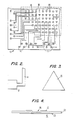
- Fig. 1 illustrates a section of the terminal pad metal layer which is deposited on a semiconductor chip 10 after the device fabrication and interconnection processes are completed.
- the type of and processes for making the semiconductor devices are not critical to this invention, nor are the methods of interconnecting the devices.
- the integrated circuit can have 1, 2, 3 or any number of metal interconnect layers under the pad level metal.
- the terminal pad metal level includes via pads 12 along the periphery of the chip 10. Via pads 12 connect through one or more underlying layers (not shown) down to underlying devices and interconnection metallurgy. Metal lines 14 carry the electrical signals from the via pads 12 to an array of terminal pads shown within the dotted area 16.
- ⁇ Within the area 16 are functional terminal pads 18 that will carry electrical signals to and from the chip 10. These functional pads 18 have a first shape which is square in the preferred embodiment. Also, within the pad array area 16 are non-functional terminal pads 20 which have a second shape which is easily distinguishable from the first square shape. In the preferred embodiment, this shape is triangular.
- Fig. 2 shows a blown-up functional terminal pad 18 with metal line 14 connecting it to a via pad (not shown).
- Fig. 3 shows a non-functional triangular terminal pad 20. Since pad 20 is non-functional, i.e., there are no inputs or outputs to it, there is no corresponding metal line attached.
- the process for depositing the pad metal level is the same as currently practiced in the art. The only difference is that the mask used to define the pad level metal has both triangular and square terminal pad shapes, rather than just one shape as currently practiced. Also, the choice of materials is the same as practiced in the art is are of no significance to This invention.
- the entire semiconductor chip is coated with a passivation/insulation layer such as polyimide.
- a passivation/insulation layer such as polyimide.
- Other passivation/insulation layers can be used, but it is preferable to use a material that is easily applied and is transparent.
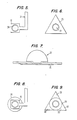
- the semiconductor chip 10 includes the terminal pad 20 which, in this case is a triangular, non-functional pad 20.
- the polyimide passivation/insulation layer 22 Applied over the pad metal layer.
- the terminal via 24 through the polyimide layer 22. The steps for this process are beyond the scope of this invention. After etching the via 24, the functional terminal pads 18 and non-functional pads 20 would appear as in Figs. 5 and 6, respectively.
- the ball limiting metallurgy 26 is deposited through appropriate masks.
- the ball limiting metallurgy which can comprise chrome, copper, titanium, gold, nickel, tungsten or any other metals conventionally used for interconnection, makes contact through the via 24 down to the underlying terminal pads 20 or 18.
- Figs. 8 and 9 illustrate the relative dimensions of the ball limiting metallurgy 24 with respect to the functional terminal pad 18 and non-functional pad 20.
- the ball limiting metallurgy 24 will define the dimensions of the solder balls which are subsequently deposited.
- the solder balls are deposited in a manner wellknown in the art, one method of which is disclosed in U.S. Patent 4,290,079, which is commonly assigned to the assignee of this invention and is hereby incorporated by reference.
- the cross-section of the semiconductor chip 10 appears as is shown in Fig. 7.
Abstract
To facilitate inspection, the pad metal level of a semiconductor chip (10) includes terminal pads having two different shapes. The terminal pads (18) that are to be functional are patterned in a first shape and the non-functional terminal pads (20) are patterned in an easily distinguishable second shape. Since the final passivation layer is transparent, the two shapes can be distinguished during inspection following the fabrication of solder balls, and rework of defective solder balls on non-functional pads can be avoided.
Description
- This invention relates to the field of semiconductor chip connections. In particular, a structure for and method of making a distinctive non-functional chip terminal pad is disclosed and claimed.
- In very large scale integrated (VLSI) circuits, the number of inputs and outputs to a semiconductor chip can be on the order of several hundreds to a thousand. To accommodate this large number of input/output (I/O) connections in a small space, a number of chip connection processes have been used successfully.
- In one method, the last level of metal interconnect wiring of a chip, known as pad metal, is patterned to include an array of terminal pads where chip I/O are desired. This last level of metal is then coated with a passivation/insulation layer, such as polyimide. Terminal vias are then patterned and etched through the passivation/insulation layer and subsequently filled with an additional layer of metal which forms a surface metallurgy or ball limiting metallurgy (BLM).
- In those applications where solder balls are used for chip I/O connections, it is common to form an array of solder balls evenly distributed on the surface of the chip to facilitate mounting and distribution of stresses evenly across the chip. However, not all of the solder balls are necessarily needed for I/O purposes on a given chip. Therefore, a number of solder balls are attached to non-functional terminal pads.
- During solder balls fabrication, occasionally some will be malformed, missing, etc. often resulting in costly rework. When the defective solder balls are formed on non-functional terminal pads, there is no need to go through the rework process. However, the identification of functional/non-functional solder balls has required the use of special microscopes or masking microscopes due to the small dimensions involved. This is a very costly, labor-intensive operation. The alternative of not depositing solder balls on non-functional pads is also not practical because this alternative would require separate deposition masks for each chip product. Furthermore, the redistribution of stresses on the functional solder balls would lead to premature failure of the solder ball connections.
- The invention as claimed solves the problem of providing a terminal pad structure that facilitates the identification of non-functional terminal pads without requiring, for instance, the use of specialized microscopes. Further, the invention provides a process for making terminal pads that can be identified without the use of specialized microscopes.
- In summary of the invention, a semiconductor chip is fabricated using standard practices up to the pad level, or last level of metal. At the pad metal level, the terminal pads that are to be functional are patterned in a first shape and the non-functional terminal pads are patterned in an easily distinguishable second shape. Since the final passivation layer is transparent, the two shapes can be distinguished during inspection following the fabrication of solder balls, and rework of defective solder balls on non-functional pads can be avoided.
- The invention will be more fully understood with reference to the description of the preferred embodiment and with reference to the drawings wherein:
- Fig. 1 is an exploded top view of a section of the pad metal level of a semiconductor chip.
- Fig. 2 is a diagrammatic view of a functional terminal pad.
- Fig. 3 is a diagrammatic view of a non-functional terminal pad.
- Fig. 4 is a cross-sectional view of a semiconductor chip showing the pad level metal and ball limiting metallurgy.
- Fig. 5 is a diagrammatic view of a functional terminal pad after terminal via etch.
- Fig. 6 is a diagrammatic view of a non-functional terminal pad after terminal via etch.
- Fig. 7 is a cross-sectional view of a semiconductor chip after a solder ball formation.
- Fig. 8 is a diagrammatic view of a functional terminal pad following solder ball fabrication.
- Fig. 9 is a diagrammatic view of a non-functional pad terminal pad after solder ball deposition.
- Fig. 1 illustrates a section of the terminal pad metal layer which is deposited on a
semiconductor chip 10 after the device fabrication and interconnection processes are completed. The type of and processes for making the semiconductor devices are not critical to this invention, nor are the methods of interconnecting the devices. For example, the integrated circuit can have 1, 2, 3 or any number of metal interconnect layers under the pad level metal. - The terminal pad metal level includes via
pads 12 along the periphery of thechip 10. Viapads 12 connect through one or more underlying layers (not shown) down to underlying devices and interconnection metallurgy.Metal lines 14 carry the electrical signals from thevia pads 12 to an array of terminal pads shown within the dotted area 16. - Within the area 16 are
functional terminal pads 18 that will carry electrical signals to and from thechip 10. Thesefunctional pads 18 have a first shape which is square in the preferred embodiment. Also, within the pad array area 16 are non-functionalterminal pads 20 which have a second shape which is easily distinguishable from the first square shape. In the preferred embodiment, this shape is triangular. - Fig. 2 shows a blown-up
functional terminal pad 18 withmetal line 14 connecting it to a via pad (not shown). Fig. 3 shows a non-functionaltriangular terminal pad 20. Sincepad 20 is non-functional, i.e., there are no inputs or outputs to it, there is no corresponding metal line attached. - The process for depositing the pad metal level is the same as currently practiced in the art. The only difference is that the mask used to define the pad level metal has both triangular and square terminal pad shapes, rather than just one shape as currently practiced. Also, the choice of materials is the same as practiced in the art is are of no significance to This invention.
- After the pad metal level is deposited, the entire semiconductor chip is coated with a passivation/insulation layer such as polyimide. Other passivation/insulation layers can be used, but it is preferable to use a material that is easily applied and is transparent.
- Referring to Fig. 4, the
semiconductor chip 10 includes theterminal pad 20 which, in this case is a triangular,non-functional pad 20. Applied over the pad metal layer is the polyimide passivation/insulation layer 22. In order to make contact through thepolyimide layer 22, it is necessary to etch terminal via 24 through thepolyimide layer 22. The steps for this process are beyond the scope of this invention. After etching thevia 24, thefunctional terminal pads 18 andnon-functional pads 20 would appear as in Figs. 5 and 6, respectively. - Referring back to Fig. 4, after the etching steps, the
ball limiting metallurgy 26 is deposited through appropriate masks. The ball limiting metallurgy, which can comprise chrome, copper, titanium, gold, nickel, tungsten or any other metals conventionally used for interconnection, makes contact through thevia 24 down to theunderlying terminal pads ball limiting metallurgy 24 with respect to thefunctional terminal pad 18 and non-functionalpad 20. Theball limiting metallurgy 24 will define the dimensions of the solder balls which are subsequently deposited. The solder balls are deposited in a manner wellknown in the art, one method of which is disclosed in U.S. Patent 4,290,079, which is commonly assigned to the assignee of this invention and is hereby incorporated by reference. The cross-section of thesemiconductor chip 10 appears as is shown in Fig. 7. - It is readily observed (Fig. 8) that when a
solder ball 27 is fabricated on top of afunctional terminal pad 18, theterminal pad 18 will no longer be visible from inspection from above due to its smaller dimension than the solder ball. Conversely, because thenon-functional pad 20 in Fig. 9 is chosen to be of a different shape with dimensions larger than the solder ball,corners 28 of thetriangular terminal pad 20 will not be covered by theball limiting metallurgy 24 or solder ball and can be readily identified when viewed through a conventional microscope. In this manner, if a solder ball is missing or defective, and an inspector observes that this solder ball lies over a non-functional pad, this defect can be ignored and costly rework can be avoided. - While the invention has been particularly shown and described with reference to a preferred embodiment thereof, it will be understood by those skilled in the art that various changes in detail may be made therein without departing from the spirit, scope and teaching of the invention. For example, the shapes and dimensions of the functional and non-functional terminal pads could be selected differently. Accordingly, the structure and process herein disclosed is to be considered merely as illustrative, and the invention is to be limited only as specified in the claims.
Claims (10)
1. In an integrated circuit having semiconductor devices and interconnection metallurgy, an improved terminal pad metal level comprising:
a pattern of terminal pads including at least one functional terminal pad (18) having a first shape and at least one non-functional terminal pad (20) having a second shape, whereby non-functional pads can be distinguished by the shape of said pads.
a pattern of terminal pads including at least one functional terminal pad (18) having a first shape and at least one non-functional terminal pad (20) having a second shape, whereby non-functional pads can be distinguished by the shape of said pads.
2. The structure as claimed in claim 1 wherein said first shape is a quadrilateral.
3. The structure as claimed in claims 1 or 2 wherein said second shape is triangular.
4. A semiconductor chip (10) device comprising:
a plurality of semiconductor devices;
at least one layer of interconnection metallurgy supplying input/output signals to said devices;
a pad metal level having a pattern of terminal pads, said pattern of terminal pads including at least one functional pad (18) having a first shape and at least one non-functional pad (20) having a second shape;
an insulating layer overlying said pad metal level;
terminal vias (12) connecting through said insulating layer;
a ball limiting layer of metal making contact through said terminal vias; and
a plurality of solder balls formed on said ball limiting layer.
5. The structure as claimed in claim 4 wherein said insulating layer is transparent for inspection from above.
6. The structure of one of the preceding claims wherein the terminal pads are of different shapes with dimensions larger relative to the respective dimension of a later applied solder ball and, respectively, smaller than said solder ball as to be no longer visible from inspection from above (Figs. 8, 9).
7. A process for fabricating integrated circuits comprising the steps of:
a) providing a semiconductor substrate having device and interconnection metallurgy;
b) depositing a terminal pad level of metal, said terminal pad level including at least one pad (18) having a first shape and at least one pad (20) having a second shape;
c) coating said terminal pad level of metal with an insulating layer;
d) defining terminal vias through said insulation layer;
e) depositing a layer of ball limiting metallurgy on said insulating layer and through said terminal vias;
f) forming solder balls for input/output connections on said ball limiting metallurgy.
8. The process as claimed in claim 5 wherein said insulating layer is polyimide.
9. The process as claimed in claims 7 or 8 wherein said insulating layer is provided in a thickness or of a material as to be transparent for inspection from above.
10. The process of one of the preceding claims wherein the terminal pads of different shapes are formed with dimensions larger relative to the respective dimension of a later applied solder ball and, respectively, smaller than said solder ball as to be no longer visible from inspection from above (Figs. 8, 9).
Applications Claiming Priority (2)
| Application Number | Priority Date | Filing Date | Title |
|---|---|---|---|
| US3419887A | 1987-04-06 | 1987-04-06 | |
| US34198 | 1987-04-06 |
Publications (2)
| Publication Number | Publication Date |
|---|---|
| EP0285820A2 true EP0285820A2 (en) | 1988-10-12 |
| EP0285820A3 EP0285820A3 (en) | 1990-06-13 |
Family
ID=21874908
Family Applications (1)
| Application Number | Title | Priority Date | Filing Date |
|---|---|---|---|
| EP88103369A Withdrawn EP0285820A3 (en) | 1987-04-06 | 1988-03-04 | Method and structure for identifying non-functional chip connect pads |
Country Status (2)
| Country | Link |
|---|---|
| EP (1) | EP0285820A3 (en) |
| JP (1) | JPS63261842A (en) |
Cited By (5)
| Publication number | Priority date | Publication date | Assignee | Title |
|---|---|---|---|---|
| EP0402592A2 (en) * | 1989-06-13 | 1990-12-19 | Kabushiki Kaisha Toshiba | Master slice semiconductor device and method of forming it |
| FR2680278A1 (en) * | 1991-08-08 | 1993-02-12 | Gemplus Card Int | Integrated circuit and use in a module with several integrated circuit chips |
| US6212077B1 (en) | 1999-01-25 | 2001-04-03 | International Business Machines Corporation | Built-in inspection template for a printed circuit |
| CN102692526A (en) * | 2011-03-23 | 2012-09-26 | 鸿富锦精密工业(深圳)有限公司 | An assistant testing device |
| US20120246371A1 (en) * | 2011-03-23 | 2012-09-27 | Hon Hai Precision Industry Co., Ltd. | Test apparatus for pci card |
Citations (2)
| Publication number | Priority date | Publication date | Assignee | Title |
|---|---|---|---|---|
| DE1964632A1 (en) * | 1968-12-31 | 1970-07-09 | Philips Nv | A method of manufacturing semiconductor components and a semiconductor plate for use as a starting material in this method |
| JPS604249A (en) * | 1983-06-22 | 1985-01-10 | Nec Corp | Semiconductor device |
-
1988
- 1988-02-03 JP JP2218188A patent/JPS63261842A/en active Pending
- 1988-03-04 EP EP88103369A patent/EP0285820A3/en not_active Withdrawn
Patent Citations (2)
| Publication number | Priority date | Publication date | Assignee | Title |
|---|---|---|---|---|
| DE1964632A1 (en) * | 1968-12-31 | 1970-07-09 | Philips Nv | A method of manufacturing semiconductor components and a semiconductor plate for use as a starting material in this method |
| JPS604249A (en) * | 1983-06-22 | 1985-01-10 | Nec Corp | Semiconductor device |
Non-Patent Citations (2)
| Title |
|---|
| IBM TECHNICAL DISCLOSURE BULLETIN, vol. 21, no. 4, September 1978, pages 1461-1462, New York, US; E. BERNDLMAIER: "Chip orientation aid" * |
| PATENT ABSTRACTS OF JAPAN, vol. 9, no. 115 (E-315)[1838], 18th May 1985; & JP-A-60 004 249 (NIPPON DENKI) * |
Cited By (8)
| Publication number | Priority date | Publication date | Assignee | Title |
|---|---|---|---|---|
| EP0402592A2 (en) * | 1989-06-13 | 1990-12-19 | Kabushiki Kaisha Toshiba | Master slice semiconductor device and method of forming it |
| EP0402592A3 (en) * | 1989-06-13 | 1991-07-24 | Kabushiki Kaisha Toshiba | Master slice semiconductor device and method of forming it |
| FR2680278A1 (en) * | 1991-08-08 | 1993-02-12 | Gemplus Card Int | Integrated circuit and use in a module with several integrated circuit chips |
| US6212077B1 (en) | 1999-01-25 | 2001-04-03 | International Business Machines Corporation | Built-in inspection template for a printed circuit |
| US6514777B2 (en) | 1999-01-25 | 2003-02-04 | International Business Machines Corporation | Built-in inspection template for a printed circuit |
| CN102692526A (en) * | 2011-03-23 | 2012-09-26 | 鸿富锦精密工业(深圳)有限公司 | An assistant testing device |
| US20120246371A1 (en) * | 2011-03-23 | 2012-09-27 | Hon Hai Precision Industry Co., Ltd. | Test apparatus for pci card |
| US20120242362A1 (en) * | 2011-03-23 | 2012-09-27 | Hon Hai Precision Industry Co., Ltd. | Test apparatus |
Also Published As
| Publication number | Publication date |
|---|---|
| EP0285820A3 (en) | 1990-06-13 |
| JPS63261842A (en) | 1988-10-28 |
Similar Documents
| Publication | Publication Date | Title |
|---|---|---|
| US4446477A (en) | Multichip thin film module | |
| US6277669B1 (en) | Wafer level packaging method and packages formed | |
| US5010389A (en) | Integrated circuit substrate with contacts thereon for a packaging structure | |
| US5244833A (en) | Method for manufacturing an integrated circuit chip bump electrode using a polymer layer and a photoresist layer | |
| US6221750B1 (en) | Fabrication of deformable leads of microelectronic elements | |
| US5847466A (en) | Semiconductor device and manufacturing method for the same | |
| EP1374306B1 (en) | Bump metallurgy bars for power and ground routing | |
| DE69915299T2 (en) | METHOD FOR TRANSLATING SOLDERING ON AN ARRANGEMENT AND / OR TESTING THE ARRANGEMENT | |
| US11495567B2 (en) | Multi-pin-wafer-level-chip-scale-packaging solution for high power semiconductor devices | |
| EP0171662A2 (en) | Method of fabricating a chip interposer | |
| KR20050085387A (en) | Method for making a socket to perform testing on integrated circuits and socket made | |
| US20060234423A1 (en) | System for providing a redistribution metal layer in an integrated circuit | |
| EP0145862B1 (en) | Metallization of a ceramic substrate | |
| EP0285820A2 (en) | Method and structure for identifying non-functional chip connect pads | |
| JP4592634B2 (en) | Semiconductor device | |
| KR100733525B1 (en) | Interconnect assemblies and methods | |
| US20060180945A1 (en) | Forming a cap above a metal layer | |
| US6667627B2 (en) | Probe for inspecting semiconductor device and method of manufacturing the same | |
| US6291268B1 (en) | Low cost method of testing a cavity-up BGA substrate | |
| US7411135B2 (en) | Contour structures to highlight inspection regions | |
| CN101150087B (en) | Device with plating through structure and its making method | |
| US6429390B1 (en) | Structure and method for forming the same of a printed wiring board having built-in inspection aids | |
| JPH03268385A (en) | Solder bump and manufacture thereof | |
| JP2006222103A (en) | Semiconductor wafer, its production process and method for inspecting semiconductor wafer | |
| JP3128200B2 (en) | Electronic circuit board inspection method |
Legal Events
| Date | Code | Title | Description |
|---|---|---|---|
| PUAI | Public reference made under article 153(3) epc to a published international application that has entered the european phase |
Free format text: ORIGINAL CODE: 0009012 |
|
| AK | Designated contracting states |
Kind code of ref document: A2 Designated state(s): DE FR GB |
|
| 17P | Request for examination filed |
Effective date: 19890222 |
|
| PUAL | Search report despatched |
Free format text: ORIGINAL CODE: 0009013 |
|
| AK | Designated contracting states |
Kind code of ref document: A3 Designated state(s): DE FR GB |
|
| STAA | Information on the status of an ep patent application or granted ep patent |
Free format text: STATUS: THE APPLICATION IS DEEMED TO BE WITHDRAWN |
|
| 18D | Application deemed to be withdrawn |
Effective date: 19901214 |