EP0285295A1 - Matched dual mode waveguide corner - Google Patents
Matched dual mode waveguide corner Download PDFInfo
- Publication number
- EP0285295A1 EP0285295A1 EP88302412A EP88302412A EP0285295A1 EP 0285295 A1 EP0285295 A1 EP 0285295A1 EP 88302412 A EP88302412 A EP 88302412A EP 88302412 A EP88302412 A EP 88302412A EP 0285295 A1 EP0285295 A1 EP 0285295A1
- Authority
- EP
- European Patent Office
- Prior art keywords
- waveguide
- corner
- reflecting
- ridges
- mode
- Prior art date
- Legal status (The legal status is an assumption and is not a legal conclusion. Google has not performed a legal analysis and makes no representation as to the accuracy of the status listed.)
- Withdrawn
Links
- 230000009977 dual effect Effects 0.000 title claims description 12
- 230000001419 dependent effect Effects 0.000 description 2
- 241000217377 Amblema plicata Species 0.000 description 1
- 238000005388 cross polarization Methods 0.000 description 1
- 230000003993 interaction Effects 0.000 description 1
- 238000002955 isolation Methods 0.000 description 1
- 239000002184 metal Substances 0.000 description 1
- 230000004048 modification Effects 0.000 description 1
- 238000012986 modification Methods 0.000 description 1
- 230000010287 polarization Effects 0.000 description 1
- 230000001902 propagating effect Effects 0.000 description 1
- 239000007787 solid Substances 0.000 description 1
Images


Classifications
-
- H—ELECTRICITY
- H01—ELECTRIC ELEMENTS
- H01P—WAVEGUIDES; RESONATORS, LINES, OR OTHER DEVICES OF THE WAVEGUIDE TYPE
- H01P1/00—Auxiliary devices
- H01P1/02—Bends; Corners; Twists
- H01P1/022—Bends; Corners; Twists in waveguides of polygonal cross-section
Definitions
- the present invention relates generally to waveguides and more particularly to a polarized mitered corner for square waveguides which provides a match for both orthogonal modes (TE10 and TE01) simultaneously.
- Square waveguides are often used in dual polarization applications, since square waveguides can support two orthogonal modes (TE10 and TE01) with identical phase velocity.
- Well matched bends or corners are often difficult to achieve, due to the complexities involved in changing the direction of propagation within the waveguide system.
- a right angle bend or corner is one of the most difficult to achieve.
- a right angle corner is implemented by constructing a mitered corner which provides a diagonally oriented reflecting surface for changing the direction of the propagating electromagnetic energy and causing it to round the corner or bend. Corners other than right angle corners are implemented in the same way.
- the simple mitered corner is ineffective. This is largely due to the fact that the TE10 mode and the TE01 mode behave differently when reflecting from the mitered corner and inherently require different miter sizes. If the mitered corner is designed for optimal E-plane performance (tuned to the TE01 mode), it will not have optimal performance for the H-plane mode, and vice versa. The prior art has failed to adequately address this problem.
- the present invention solves the aforementioned problem by providing a waveguide corner which is matched for dual mode operation.
- the invention provides first and second waveguides, such as square waveguides which are each capable of supporting two orthogonal modes of electromagnetic energy propagation simultaneously.
- the waveguides are joined together to define a corner.
- a reflecting means is positioned in the corner for reflecting the electromagnetic energy from the first waveguide to the second waveguide.
- the reflecting means has at least two polarized reflecting surfaces which are disposed in different transverse planes. One of the reflecting surfaces reflects one of the two orthogonal modes, while the other reflecting surface reflects the other of the orthogonal modes. Because the two reflecting surfaces lie in different transverse planes, they can each be designed for optimal performance, one for the E-plane and the other for the H-plane.
- the reflecting means herein comprises a reflecting plane with at least one, and preferably several, elongated ridges projecting outwardly from the reflecting plane.
- the ridges are oriented generally parallel to one of the sidewalls, so that the mode having an E-field parallel to the ridges will reflect from the ridges, while the mode having an E-field perpendicular to the ridges, will propagate between the ridges and will reflect from the backwall on which the ridges are formed.
- the reflecting planes are comprised of a plurality of conductive wires parallel to one another and located in two planes which are also parallel to one another.
- FIG. 2 a prior art square waveguide right angle corner 10, shown in FIG. 2, which is constructed by joining first and second square waveguides 12 and 14 to from a right angle bend.
- the corner defines an inside corner 16 and an outside corner 18 where the two waveguides meet.
- a wedge-shaped reflecting means 20 Positioned in the outside corner 18 is a wedge-shaped reflecting means 20 which has a reflecting surface 22 which lies in a plane forming a 45 degree angle "a" with the plane of the upstanding sidewalls 24.
- the reflecting means 20 thus defines a mitered corner whose miter size is given by the dimension L.
- Square waveguides 12 and 14 are both capable of supporting two orthogonal modes of electromagnetic energy propagation simultaneously. These modes are the TE10 mode or the H-plane mode and the TE01 mode or the E-plane mode.
- FIGS. 1A and 1B illustrate the electric (solid) and magnetic (dashed) field configurations for the TE10 and TE01 modes. It will be seen that these two modes have essentially the same field configurations but oriented 90 degrees from one another.
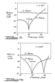
- FIGS. 3 and 4 illustrate the way in which miter size affects the signal return loss as a function of frequency for L values which have been optimized for the E-plane and the H-plane modes respectively. These curves are representative of the results obtained using an X-band square waveguide corner of the configuration shown in FIG. 2.
- FIG. 3 depicts the return loss as a function of frequency for a miter size of 0.700 inches (each sidewall of the waveguide being 0.900 inches).
- FIG. 4 illustrates the results obtained using a miter size of 0.642 inches.
- the former case represents a corner which is tuned to provide an E-plane match, where as the latter case represents a corner tuned to provide an H-plane match. As seen by comparing FIGS.
- the former case gives high return loss in the E-plane at the tuned frequency of approximately 7.95 GHz.
- the H-plane return loss is quite low in the former case. In the latter case, the H-plane return loss is at a maximum at 7.95 GHz, but the E-plane return loss at that frequency is comparatively low.
- the E-plane return loss is maximum at a comparatively higher frequency around 9 GHz.
- FIGS. 3 and 4 thus illustrate that in a conventional square waveguide mitered corner, the optimum miter size is not the same for the TE01 mode (E-plane) and the TE10 mode (H-plane).
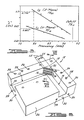
- FIG. 5 illustrates experimentally determined design curves for such mitered corners, also illustrating that the optimum miter size depends upon which mode is being used.
- FIGS. 6, 7 and 8 depict the invention and illustrate its improved performance.
- the invention comprises first and second square waveguides 12 and 14 which are joined to form a corner designated generally at 15, and comprising an inside corner 16 and an outside corner 18.
- the waveguides and corner can be implemented using a metal block 26 which is machined to provide the requisite waveguides and corners described.
- the waveguide block 26 of FIG. 6 would also have a top wall (not shown) which covers the block 26 includes a plurality of studs 28 and holes 30 for securing the cover in proper position.
- the dual mode waveguide corner employs a polarized reflecting corner 32.
- Corner 32 has a plurality of horizontal ridges 34 which project outwardly from the backplane 36 of the corner. Ridges 34 are parallel to one another and spaced apart a distance such that propagation between the ridges is cutoff for the mode of propagation in which the E-field is oriented parallel to the ridges.
- Backplane 36 defines a first reflecting surface 38 and the vertical walls of ridges 34 define a second reflecting surface 40.
- reflecting surfaces 38 and 40 are disposed in different transverse planes 42 and 44. Reflecting surfaces 38 and 40 are spaced apart a distance d.
- the polarized reflecting corner is constructed so that one of the orthogonal modes (the TE10 or H-plane mode) reflects from the first reflecting surface defined by backplane 36, while the other mode (the TE01 or E-plane mode) reflects from the second reflecting surface 40 of ridges 34. Because of the spacing d between the two reflecting surfaces 38 and 40, the effective miter size for the H-plane is different than that of the E-plane.
- the incremental difference in miter size between the H-plane and the E-plane is determined by the spacing d divided by the sine of the miter angle a.
- the effective shorting plane will be slightly behind the ridge tops, i.e. reflecting surface 40.
- the TE10 mode which has the E-field perpendicular to the ridges, is little influenced by the ridges and the effective shorting plane is approximately the original backplane reflecting surface 38.
- the values for miter size L, set forth in FIG. 5, can be used for a close approximation to design the reflecting surfaces for proper match in both modes.
- FIG. 8 illustrates an optimized, matched dual mode square waveguide corner using the principles of the invention.
- the curves in FIG. 8 were produced using an effective miter size L E of 0.695 inches and an effective miter size L H of 0.630 inches.
- both the E-plane and the H-plane have a high return loss at the design frequency of 7.95 GHz. Comparing these optimized miter size values (L E and L H ) with the values obtainable from FIG. 5, it will be seen that the optimized values used to produce the curves of FIG. 8 do not exactly match those of FIG. 5. This is because there is a slight amount of interaction between the reflecting surface 38 and the reflecting surface 40. Thus in some instances, a minimal design iteration may be necessary to produce optimal results.
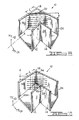
- FIGS. 9 and 10 the two parallel planes of wires (90 and 94) are separated by a distance d analogous to the distance d shown in FIG. 7.
Landscapes
- Aerials With Secondary Devices (AREA)
- Control Of Motors That Do Not Use Commutators (AREA)
Abstract
A polarized, mitered corner is constructed using a multiple surface reflector (32) in a square waveguide corner (15). The multiple surface reflector provides a mitered corner having one effective miter size for the E-plane mode and a different effective miter size for the H-plane mode. The surfaces may comprise ridges (34) which are parallel to the E-field in one of the two modes, so that the ridges behave as the reflecting surface (40) for that mode while the backplane (36), upon which the ridges are formed, serves as the reflecting surface (38) for the other mode. An alternate embodiment wherein the two reflecting surface comprise a plurality of parallel wires, is also disclosed. 
Description
- The present invention relates generally to waveguides and more particularly to a polarized mitered corner for square waveguides which provides a match for both orthogonal modes (TE₁₀ and TE₀₁) simultaneously.
- Square waveguides are often used in dual polarization applications, since square waveguides can support two orthogonal modes (TE₁₀ and TE₀₁) with identical phase velocity. In constructing practical waveguide systems, it is often necessary to provide a bend or corner where two sections of waveguide join at some angle other than a straight line. Well matched bends or corners are often difficult to achieve, due to the complexities involved in changing the direction of propagation within the waveguide system. A right angle bend or corner is one of the most difficult to achieve. Traditionally, a right angle corner is implemented by constructing a mitered corner which provides a diagonally oriented reflecting surface for changing the direction of the propagating electromagnetic energy and causing it to round the corner or bend. Corners other than right angle corners are implemented in the same way.
- There can be a great deal of mismatch associated with each corner or bend in the waveguide system. To minimize this mismatch, the traditional mitered corner is carefully tuned by selecting the proper miter size for minimum mismatch. Although this can be done in rectangular waveguide systems which are designed to support a single propagation mode (typically the TE₁₀ mode), the same is not true for square waveguides designed for dual mode operation.
- In square waveguide systems for simultaneously supporting dual propagation modes, the simple mitered corner is ineffective. This is largely due to the fact that the TE₁₀ mode and the TE₀₁ mode behave differently when reflecting from the mitered corner and inherently require different miter sizes. If the mitered corner is designed for optimal E-plane performance (tuned to the TE₀₁ mode), it will not have optimal performance for the H-plane mode, and vice versa. The prior art has failed to adequately address this problem.
- The present invention solves the aforementioned problem by providing a waveguide corner which is matched for dual mode operation. The invention provides first and second waveguides, such as square waveguides which are each capable of supporting two orthogonal modes of electromagnetic energy propagation simultaneously. The waveguides are joined together to define a corner. A reflecting means is positioned in the corner for reflecting the electromagnetic energy from the first waveguide to the second waveguide. The reflecting means has at least two polarized reflecting surfaces which are disposed in different transverse planes. One of the reflecting surfaces reflects one of the two orthogonal modes, while the other reflecting surface reflects the other of the orthogonal modes. Because the two reflecting surfaces lie in different transverse planes, they can each be designed for optimal performance, one for the E-plane and the other for the H-plane.
- The reflecting means herein comprises a reflecting plane with at least one, and preferably several, elongated ridges projecting outwardly from the reflecting plane. The ridges are oriented generally parallel to one of the sidewalls, so that the mode having an E-field parallel to the ridges will reflect from the ridges, while the mode having an E-field perpendicular to the ridges, will propagate between the ridges and will reflect from the backwall on which the ridges are formed.
- In an alternate embodiment, the reflecting planes are comprised of a plurality of conductive wires parallel to one another and located in two planes which are also parallel to one another.
- For a more complete understanding of the invention, its objects and advantages, reference may be had to the following specification and to the accompanying drawings.
-
- FIGS. 1A and 1B are cross-sectional views looking into the mouth of a square waveguide, FIG. 1A illustrating the fields of the TE₁₀ mode and FIG. 1B illustrating the fields of the TE₀₁ mode;
- FIG. 2 is a diagrammatic cross-sectional view of a prior art square corner, useful in explaining fundamental terminology;
- FIG. 3 is a graph of return loss versus frequency for a given mitered corner of the prior art optimized for the E-plane mode;
- FIG. 4 is a similar graph of return loss versus frequency for a different mitered corner of the prior art optimized for the H-plane mode;
- FIG. 5 is a graph of miter size versus frequency, illustrating the manner in which the miter size independently affects the TE₀₁ and TE₁₀ modes;
- FIG. 6 is a perspective view of the matched dual mode waveguide corner of the invention, with the top wall removed for illustration purposes;
- FIG. 7 is a cross-sectional view taken along the line VII-VII of FIG. 6 and illustrating the polarized, mitered corner in greater detail;
- FIG. 8 is a graph of return loss versus frequency for the matched dual mode waveguide corner of the invention.
- FIG. 9 illustrates an alternate embodiment wherein a plane of parallel wires replaces the ridges shown in FIG. 6 and FIG. 7; and
- FIG. 10 shows use of two such planes of wires to serve as the required two reflecting surfaces.
- In order to provide a basis for understanding the invention, reference will first be made to a prior art square waveguide
right angle corner 10, shown in FIG. 2, which is constructed by joining first and secondsquare waveguides inside corner 16 and anoutside corner 18 where the two waveguides meet. Positioned in theoutside corner 18 is a wedge-shaped reflecting means 20 which has a reflectingsurface 22 which lies in a plane forming a 45 degree angle "a" with the plane of theupstanding sidewalls 24. The reflectingmeans 20 thus defines a mitered corner whose miter size is given by the dimension L. -
Square waveguides - For purposes of illustration, assume that both modes, TE₁₀ and TE₀₁ are introduced into the mouth of
waveguide 12. Energy will be reflected back to the mouth ofwaveguide 12 for both modes. The presence of such reflected energy indicates a nonperfect match. The greater the amount of reflected energy, the less perfect is the match. The ratio of the amount of energy entering the mouth to the amount of energy reflected back to the mouth is called the "return loss." High values of return loss indicate a good match, i.e. a desirable condition. The return loss is frequency dependent and also dependent upon the miter size L. - FIGS. 3 and 4 illustrate the way in which miter size affects the signal return loss as a function of frequency for L values which have been optimized for the E-plane and the H-plane modes respectively. These curves are representative of the results obtained using an X-band square waveguide corner of the configuration shown in FIG. 2. FIG. 3 depicts the return loss as a function of frequency for a miter size of 0.700 inches (each sidewall of the waveguide being 0.900 inches). FIG. 4 illustrates the results obtained using a miter size of 0.642 inches. The former case represents a corner which is tuned to provide an E-plane match, where as the latter case represents a corner tuned to provide an H-plane match. As seen by comparing FIGS. 3 and 4, the former case gives high return loss in the E-plane at the tuned frequency of approximately 7.95 GHz. The H-plane return loss is quite low in the former case. In the latter case, the H-plane return loss is at a maximum at 7.95 GHz, but the E-plane return loss at that frequency is comparatively low. The E-plane return loss is maximum at a comparatively higher frequency around 9 GHz.
- FIGS. 3 and 4 thus illustrate that in a conventional square waveguide mitered corner, the optimum miter size is not the same for the TE₀₁ mode (E-plane) and the TE₁₀ mode (H-plane). FIG. 5 illustrates experimentally determined design curves for such mitered corners, also illustrating that the optimum miter size depends upon which mode is being used.
- With this understanding of the prior art in mind, reference will now be made to FIGS. 6, 7 and 8 which depict the invention and illustrate its improved performance. Referring to FIG. 6, the invention comprises first and second
square waveguides inside corner 16 and anoutside corner 18. As illustrated in FIG. 6, the waveguides and corner can be implemented using ametal block 26 which is machined to provide the requisite waveguides and corners described. It will be understood that thewaveguide block 26 of FIG. 6 would also have a top wall (not shown) which covers theblock 26 includes a plurality ofstuds 28 and holes 30 for securing the cover in proper position. - With reference to FIG. 7 and continued reference to FIG. 6, the dual mode waveguide corner employs a polarized reflecting corner 32. Corner 32 has a plurality of horizontal ridges 34 which project outwardly from the
backplane 36 of the corner. Ridges 34 are parallel to one another and spaced apart a distance such that propagation between the ridges is cutoff for the mode of propagation in which the E-field is oriented parallel to the ridges.Backplane 36 defines a first reflectingsurface 38 and the vertical walls of ridges 34 define a second reflectingsurface 40. - As best seen in FIG. 7, reflecting
surfaces transverse planes surfaces backplane 36, while the other mode (the TE₀₁ or E-plane mode) reflects from the second reflectingsurface 40 of ridges 34. Because of the spacing d between the two reflectingsurfaces - Using trigonometry, it can be shown that the incremental difference in miter size between the H-plane and the E-plane is determined by the spacing d divided by the sine of the miter angle a.
- By using the polarized reflecting corner 32 with raised ridges 34 oriented parallel to the E-field of the TE₀₁ mode, the effective shorting plane will be slightly behind the ridge tops, i.e. reflecting
surface 40. The TE₁₀ mode, which has the E-field perpendicular to the ridges, is little influenced by the ridges and the effective shorting plane is approximately the originalbackplane reflecting surface 38. This produces an effective miter angle LE for the TE₀₁ mode which is larger than the effective miter size LH for the TE₁₀ mode. The values for miter size L, set forth in FIG. 5, can be used for a close approximation to design the reflecting surfaces for proper match in both modes. - FIG. 8 illustrates an optimized, matched dual mode square waveguide corner using the principles of the invention. The curves in FIG. 8 were produced using an effective miter size LE of 0.695 inches and an effective miter size LH of 0.630 inches. As seen in FIG. 8, both the E-plane and the H-plane have a high return loss at the design frequency of 7.95 GHz. Comparing these optimized miter size values (LE and LH) with the values obtainable from FIG. 5, it will be seen that the optimized values used to produce the curves of FIG. 8 do not exactly match those of FIG. 5. This is because there is a slight amount of interaction between the reflecting
surface 38 and the reflectingsurface 40. Thus in some instances, a minimal design iteration may be necessary to produce optimal results. - Using the corner illustrated in FIG. 5 with the stated miter sized for producing the results of FIG. 8, dual mode operation of the corner at 7.95 GHz showed a VSWR of less than 1.05 for both E-plane and H-plane operation over a band of approximately 1.0 GHz. Cross-polarization isolation was typically 30 dB across the 7 to 9.6 GHz band.
- While the invention has been illustrated in connection with a particular 90 degree mitered corner with a three-ridge reflector, it will be understood that the principles of the invention can be applied to a broad range of other configurations. An example of such other configurations is the use of a set (90 or 94) of parallel small gauge wires, forming a grid in a position to replace the tops of the physical ridges illustrated in FIGS. 6 and 7. Such sets of
parallel wires 95 are shown in FIGS. 9 and 10. In FIG. 10, the two parallel planes of wires (90 and 94) are separated by a distance d analogous to the distance d shown in FIG. 7. In general, the use of more, but thinner ridges (wires) will provide a more precise correlation of measured results and the results plotted in FIG. 5. Accordingly, the invention is capable of certain modification and change without departing from the spirit of the invention as set forth in the appended claims.
Claims (19)
1. A matched dual mode waveguide corner comprising:
first and second waveguide each for supporting two orthogonal modes of electromagnetic energy propagation;
said first and second waveguides being joined together to define a corner;
a reflecting means positioned in said corner for reflecting said electromagnetic energy from said first waveguide to said second waveguide;
said reflecting means having at least two polarized reflecting surfaces disposed in different transverse planes, wherein a first one of said reflecting surfaces reflects one of said orthogonal modes of electromagnetic energy and wherein a second one of said reflecting surfaces reflects the other of said orthogonal modes of electromagnetic energy.
first and second waveguide each for supporting two orthogonal modes of electromagnetic energy propagation;
said first and second waveguides being joined together to define a corner;
a reflecting means positioned in said corner for reflecting said electromagnetic energy from said first waveguide to said second waveguide;
said reflecting means having at least two polarized reflecting surfaces disposed in different transverse planes, wherein a first one of said reflecting surfaces reflects one of said orthogonal modes of electromagnetic energy and wherein a second one of said reflecting surfaces reflects the other of said orthogonal modes of electromagnetic energy.
2. The waveguide corner of Claim 1 wherein said first and second waveguides are both square waveguides.
3. The waveguide corner of Claim 1 wherein said corner is a ninety degree corner.
4. The waveguide corner of Claim 1 wherein said waveguides have orthogonal sidewalls and said reflecting means comprises a reflecting plane and at least one elongated ridge projecting outwardly from said reflecting plane, said ridge being orientated generally parallel to one of said sidewalls.
5. The waveguide corner of Claim 2 wherein said waveguide have orthogonal sidewalls and wherein said reflecting surfaces are disposed in transverse planes which are orthogonal to at least one of said sidewalls.
6. The waveguide corner of Claim 1 wherein said waveguides each simultaneously support two orthogonal modes of electromagnetic energy propagation.
7. The waveguide corner of Claim 1 wherein said waveguides each support the TE₁₀ mode and the TE₀₁ mode.
8. The waveguide corner of Claim 1 wherein said first reflecting surface is a predetermined first distance from a reference point on said corner and said second reflecting surface is a predetermined second distance from said reference point, said first and second distances being such that the tuned frequency of said waveguide corner is substantially the same for both of said orthogonal modes.
9. The waveguide corner of Claim 1 wherein said reflecting means includes a plurality of spaced apart parallel ridges.
10. The waveguide corner of Claim 9 wherein said ridges are spaced apart a distance such that propagation between said ridges is cutoff for the mode of propagation in which the E-field is oriented parallel to said ridges.
11. A matched dual mode waveguide comprising:
at least one waveguide for supporting at least two orthogonal modes of electromagnetic energy propagation and for defining an energy propagation path;
a reflecting means positioned in said waveguide for redirecting said propagation path;
said reflecting means defining a backplane and having at least one ridge means extending outwardly from said backplane;
said backplane providing a first reflecting surface for one of said orthogonal modes and said ridge means providing a second reflecting surface for another of said orthogonal modes.
at least one waveguide for supporting at least two orthogonal modes of electromagnetic energy propagation and for defining an energy propagation path;
a reflecting means positioned in said waveguide for redirecting said propagation path;
said reflecting means defining a backplane and having at least one ridge means extending outwardly from said backplane;
said backplane providing a first reflecting surface for one of said orthogonal modes and said ridge means providing a second reflecting surface for another of said orthogonal modes.
12. The waveguide of Claim 11 wherein said first and second reflecting surfaces lie in different planes.
13. The waveguide of Claim 11 wherein said first and second reflecting surfaces lie in different parallel planes.
14. The waveguide of Claim 11 wherein said waveguide is a square waveguide.
15. The waveguide of Claim 11 wherein said waveguide has orthogonal sidewalls and said ridge means is oriented generally parallel to one of said sidewalls.
16. The waveguide of Claim 11 wherein said reflecting means has a plurality of ridges extending outwardly from said backplane.
17. The waveguide of Claim 11 wherein said reflecting means has a plurality of parallel and spaced apart ridges extending outwardly from said backplane.
18. The waveguide of Claim 17 wherein said ridges are spaced apart a distance such that propagation between said ridges is cutoff for a mode of propagation in which the E-field is oriented parallel to said ridges.
19. The waveguide corner of Claim 1 wherein said reflecting means includes a plurality of spaced apart parallel wires.
Applications Claiming Priority (2)
| Application Number | Priority Date | Filing Date | Title |
|---|---|---|---|
| US30767 | 1987-03-26 | ||
| US07/030,767 US4795993A (en) | 1987-03-26 | 1987-03-26 | Matched dual mode waveguide corner |
Publications (1)
| Publication Number | Publication Date |
|---|---|
| EP0285295A1 true EP0285295A1 (en) | 1988-10-05 |
Family
ID=21855912
Family Applications (1)
| Application Number | Title | Priority Date | Filing Date |
|---|---|---|---|
| EP88302412A Withdrawn EP0285295A1 (en) | 1987-03-26 | 1988-03-18 | Matched dual mode waveguide corner |
Country Status (3)
| Country | Link |
|---|---|
| US (1) | US4795993A (en) |
| EP (1) | EP0285295A1 (en) |
| IL (1) | IL85573A0 (en) |
Cited By (4)
| Publication number | Priority date | Publication date | Assignee | Title |
|---|---|---|---|---|
| FR2655204A1 (en) * | 1989-11-27 | 1991-05-31 | Matsushita Electric Works Ltd | WAVEGUIDE SUPPLY NETWORK ANTENNA. |
| WO1999026310A1 (en) * | 1997-11-13 | 1999-05-27 | Carnegie Mellon University | Wireless signal distribution in a building hvac system |
| US5977851A (en) * | 1997-11-13 | 1999-11-02 | Carnegie Mellon University | Wireless signal distribution in a building HVAC system |
| EP1881551A1 (en) | 2006-07-20 | 2008-01-23 | Kathrein-Werke KG | Wave guide manifold |
Families Citing this family (8)
| Publication number | Priority date | Publication date | Assignee | Title |
|---|---|---|---|---|
| JP2526537B2 (en) | 1991-08-30 | 1996-08-21 | 日本電装株式会社 | Pipe energy supply system |
| US7888134B2 (en) * | 2003-06-05 | 2011-02-15 | Oakland University | Immunosensors: scFv-linker design for surface immobilization |
| JP2009010844A (en) * | 2007-06-29 | 2009-01-15 | New Industry Research Organization | Waveguide |
| US8244287B2 (en) * | 2009-10-29 | 2012-08-14 | Z-Communications, Inc. | Radio and antenna system and dual-mode microwave coupler |
| US8988294B2 (en) | 2011-12-06 | 2015-03-24 | Viasat, Inc. | Antenna with integrated condensation control system |
| US9859597B2 (en) | 2015-05-27 | 2018-01-02 | Viasat, Inc. | Partial dielectric loaded septum polarizer |
| US9640847B2 (en) | 2015-05-27 | 2017-05-02 | Viasat, Inc. | Partial dielectric loaded septum polarizer |
| CN106450748A (en) * | 2016-11-08 | 2017-02-22 | 广东盛路通信科技股份有限公司 | Cavity coupling slot radiation unit |
Citations (3)
| Publication number | Priority date | Publication date | Assignee | Title |
|---|---|---|---|---|
| GB675118A (en) * | 1949-11-08 | 1952-07-02 | Vickers Electrical Co Ltd | Improvements relating to electrical waveguides |
| US2640877A (en) * | 1947-04-17 | 1953-06-02 | Gen Electric | Wave guide elbow joint |
| US2985852A (en) * | 1956-01-04 | 1961-05-23 | Gen Electric Co Ltd | Apparatus of the kind including a waveguide |
Family Cites Families (7)
| Publication number | Priority date | Publication date | Assignee | Title |
|---|---|---|---|---|
| US2364371A (en) * | 1940-08-31 | 1944-12-05 | Rca Corp | Double polarization feed for horn antennas |
| FR1082769A (en) * | 1953-05-22 | 1955-01-03 | Csf | Advanced amplitude modulator, especially for millimeter waves |
| US2829352A (en) * | 1953-12-24 | 1958-04-01 | Varian Associates | Tunable waveguide short |
| US3087130A (en) * | 1962-03-08 | 1963-04-23 | Bell Telephone Labor Inc | Waveguide elbow |
| US3219955A (en) * | 1962-11-06 | 1965-11-23 | Showa Electric Wire & Cable Co | Bend for circular waveguide utilizing mode suppressing subdividing partitions |
| US3327250A (en) * | 1964-11-16 | 1967-06-20 | Technical Appliance Corp | Multi-mode broad-band selective coupler |
| DE2424010C2 (en) * | 1974-05-17 | 1983-08-25 | AEG-Telefunken Nachrichtentechnik GmbH, 7150 Backnang | Waveguide angle bent over the narrow side |
-
1987
- 1987-03-26 US US07/030,767 patent/US4795993A/en not_active Expired - Lifetime
-
1988
- 1988-02-29 IL IL85573A patent/IL85573A0/en unknown
- 1988-03-18 EP EP88302412A patent/EP0285295A1/en not_active Withdrawn
Patent Citations (3)
| Publication number | Priority date | Publication date | Assignee | Title |
|---|---|---|---|---|
| US2640877A (en) * | 1947-04-17 | 1953-06-02 | Gen Electric | Wave guide elbow joint |
| GB675118A (en) * | 1949-11-08 | 1952-07-02 | Vickers Electrical Co Ltd | Improvements relating to electrical waveguides |
| US2985852A (en) * | 1956-01-04 | 1961-05-23 | Gen Electric Co Ltd | Apparatus of the kind including a waveguide |
Non-Patent Citations (2)
| Title |
|---|
| 1986 IEEE-MTT-S INTERNATIONAL MICROWAVE SYMPOSIUM DIGEST, 2nd-4th June 1986, pages 155-156, IEEE, New York, US; P.K. PARK et al.: "Matched, dual mode square waveguide corner" * |
| MICROWAVE JOURNAL, vol. 29, no. 11, November 1986, pages 153-154,156, Dehdam, Massachusetts, US; P.K. PARK et al.: "Matched, dual mode square waveguide corner" * |
Cited By (7)
| Publication number | Priority date | Publication date | Assignee | Title |
|---|---|---|---|---|
| FR2655204A1 (en) * | 1989-11-27 | 1991-05-31 | Matsushita Electric Works Ltd | WAVEGUIDE SUPPLY NETWORK ANTENNA. |
| WO1999026310A1 (en) * | 1997-11-13 | 1999-05-27 | Carnegie Mellon University | Wireless signal distribution in a building hvac system |
| US5977851A (en) * | 1997-11-13 | 1999-11-02 | Carnegie Mellon University | Wireless signal distribution in a building HVAC system |
| US5994984A (en) * | 1997-11-13 | 1999-11-30 | Carnegie Mellon University | Wireless signal distribution in a building HVAC system |
| EP1881551A1 (en) | 2006-07-20 | 2008-01-23 | Kathrein-Werke KG | Wave guide manifold |
| DE102006033703A1 (en) * | 2006-07-20 | 2008-01-24 | Kathrein-Werke Kg | waveguide bend |
| US7750763B2 (en) | 2006-07-20 | 2010-07-06 | Kathrein-Werke Kg | Waveguide bend having a square shape cross-section |
Also Published As
| Publication number | Publication date |
|---|---|
| IL85573A0 (en) | 1988-08-31 |
| US4795993A (en) | 1989-01-03 |
Similar Documents
| Publication | Publication Date | Title |
|---|---|---|
| US5349363A (en) | Antenna array configurations employing continuous transverse stub elements | |
| US4795993A (en) | Matched dual mode waveguide corner | |
| US4689584A (en) | Dielectric slab circulators | |
| US4380014A (en) | Feed horn for reflector antennae | |
| US4573056A (en) | Dipole radiator excited by a shielded slot line | |
| US6861997B2 (en) | Parallel plate septum polarizer for low profile antenna applications | |
| JPH0246004A (en) | Square waveguide slot array antenna | |
| JP6559385B2 (en) | Polarization separation circuit | |
| EP0834953B1 (en) | Orthogonal polarized wave branching filter and its manufacturing method | |
| US5995057A (en) | Dual mode horn reflector antenna | |
| US3031661A (en) | Microwave antenna feed for circular polarization | |
| EP0290508B1 (en) | Orthogonal mode electromagnetic wave launcher | |
| WO1996009662A1 (en) | Continuous transverse stub element devices and methods of making same | |
| US4849720A (en) | Orthogonal mode tee | |
| US4673905A (en) | Corrugated elliptical waveguide or horn | |
| WO2001043219A1 (en) | Generator of circularly polarized wave | |
| US4502053A (en) | Circularly polarized electromagnetic-wave radiator | |
| CN116598783B (en) | Air waveguide array antenna with sawtooth structure | |
| US4490696A (en) | Crossed waveguide type polarization separator | |
| US7215222B2 (en) | Dual polarization waveguide probe system with wedge shape polarization rotator | |
| US6323816B1 (en) | Sector beam antenna with scattering component | |
| JPH0247610Y2 (en) | ||
| WO2025154116A1 (en) | T-branch waveguide and antenna device | |
| EP1181735B1 (en) | Waveguide polarisation rotator | |
| JPH0654844B2 (en) | Planar antenna |
Legal Events
| Date | Code | Title | Description |
|---|---|---|---|
| PUAI | Public reference made under article 153(3) epc to a published international application that has entered the european phase |
Free format text: ORIGINAL CODE: 0009012 |
|
| STAA | Information on the status of an ep patent application or granted ep patent |
Free format text: STATUS: THE APPLICATION HAS BEEN WITHDRAWN |
|
| AK | Designated contracting states |
Kind code of ref document: A1 Designated state(s): DE FR GB IT |
|
| 18W | Application withdrawn |
Withdrawal date: 19880828 |