EP0284571A2 - Geschalteter Spannungsregler für eine Schnittstellenschaltung in einer Fernsprech-Teilnehmerschaltung - Google Patents
Geschalteter Spannungsregler für eine Schnittstellenschaltung in einer Fernsprech-Teilnehmerschaltung Download PDFInfo
- Publication number
- EP0284571A2 EP0284571A2 EP88830096A EP88830096A EP0284571A2 EP 0284571 A2 EP0284571 A2 EP 0284571A2 EP 88830096 A EP88830096 A EP 88830096A EP 88830096 A EP88830096 A EP 88830096A EP 0284571 A2 EP0284571 A2 EP 0284571A2
- Authority
- EP
- European Patent Office
- Prior art keywords
- input
- transistor
- state sensor
- storage cell
- output
- Prior art date
- Legal status (The legal status is an assumption and is not a legal conclusion. Google has not performed a legal analysis and makes no representation as to the accuracy of the status listed.)
- Granted
Links
- 210000000352 storage cell Anatomy 0.000 claims abstract description 30
- 230000009977 dual effect Effects 0.000 claims abstract description 3
- 210000004027 cell Anatomy 0.000 claims description 7
- 230000008901 benefit Effects 0.000 description 5
- 230000001052 transient effect Effects 0.000 description 4
- 239000003990 capacitor Substances 0.000 description 3
- 238000010586 diagram Methods 0.000 description 2
- 230000005540 biological transmission Effects 0.000 description 1
- 230000009849 deactivation Effects 0.000 description 1
- 238000000605 extraction Methods 0.000 description 1
- 230000000977 initiatory effect Effects 0.000 description 1
- 238000002347 injection Methods 0.000 description 1
- 239000007924 injection Substances 0.000 description 1
- 229920006395 saturated elastomer Polymers 0.000 description 1
Images


Classifications
-
- H—ELECTRICITY
- H04—ELECTRIC COMMUNICATION TECHNIQUE
- H04M—TELEPHONIC COMMUNICATION
- H04M19/00—Current supply arrangements for telephone systems
- H04M19/001—Current supply source at the exchanger providing current to substations
- H04M19/008—Using DC/DC converters
Definitions
- This invention relates to a so-called "switching" voltage regulator for an interface circuit in a telephone subscriber line, which regulator is of a type controlling the on/off states of an electronic switch connected in said circuit and comprising first and second transistors, interconnected into a so-called Darlington arrangement.
- Voltage regulators of the above-noted type are employed in electronic interfacing circuits designed to drive voice transmissions over a telephone subscriber line.
- Such regulators require, moreover, that the electric current draw for said power supplies be minimized, and particularly so the high-tension supply, reducing as a result the amount of dissipated power.
- Conventional regulators of the type noted above usually comprise a circuit portion operative to regulate the high tension supply to an interfacing circuit in a subscriber line by turning on and off an electronic switch connected to said interface circuit.
- a voltage regulator of the switching type and adapted to power an interface circuit referred to in the trade as a SLIC (Subscriber Line Interface Circuit) AMD comprises a hysteresis comparator to the non-inverting input whereof a control signal is applied to turn on and off an electronic switch formed by a pair of npn transistors connected to each other into a so-called Darlington arrangement.
- This arrangement consists of interconnecting the collectors of the first and second transistors forming said pair, and of further connecting the emitter of the second transistor to the base of the first transistor.
- the base of the second transistor is connected to a current source and to a triad of circuit devices respectively adapted to extract electric charges, extract current, and inject electric charges.
- a charge extracting device is the equivalent of a current extractor which is only activated for a given time period to produce extraction of a predetermined quantity of electric charges from the base of the second transistor.
- the comparator As the comparator is input a signal exceeding a threshold value, it will output an enable signal to the charge extracting device which turns the second transistor off.
- the enable signal is also supplied to the current extracting device which, by drawing the current I supplied continuously from the cited current source connected to the base of the second transistor, will hold said second transistor in the off state.
- the enable signal is also supplied to the charge injection device through an inverter, with consequent deactivation of that device.
- a low logic value voltage signal applied to the comparator input causes its output to be changed over and the charge and current extractor devices consequently deactivated, to the benefit of the charge injector device and current source which will turn on the transistor pair forming the switch connected to the subscriber line interface circuit.
- the charge injector device would be required, while the other devices could be left in their off state.
- the technical problem underlying this invention is to provide a so-called switching voltage regulator which affords the ability to change over an electronic switch with a low current draw and irrespective of the transient on or off phase of the switch, thereby obviating the drawbacks noted above in connection with the background art.
- a so-called switching voltage regulator as indicated being characterized in that it comprises: an ON-state sensor connected to the collector input of the first transistor; an OFF-state sensor connected to the base input of the first transistor; a pair of current extractor devices respectively associated with the related bases of the first and second transistor; first and second current sources, being each connected to a corresponding current amplifier and a third hold current source, the first of said amplifiers being connected to both said extractor devices and the second amplifier and said hold current source being connected to the base of the second transistor; first and second dual input logic AND gates, the first gate having an input associated with the output of said OFF-state sensor via a storage cell, and the second gate having an input associated with the output of said ON-state sensor via a further storage cell; each said amplifiers being respectively tied operatively to the outputs of the first and second logic gates, each logic gate receiving at the other input an appropriate regulator enable signal and said hold current source being tied operatively directly to the enable signal supplied to the second logic gate.
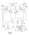
- the numeral 1 designates, comprehensively and schematically, a voltage regulator of the so-called "switching" type.
- the regulator 1 comprises a circuit portion 2 adapted to control the on/off states of an electronic switch SW connected to a telephone subscriber line interface circuit 16.
- This interface circuit is shown in the drawing limited to a resistive load represented by a resistor R L .
- the supply voltage V B has a high value, in the exemplary embodiment being described that value being -50 Volts, and powers the regulator 1 itself, which is also associated with a supply pole pair, V C and V E , at a low value equal to +/-5 V, respectively.
- Such components comprise a capacitor CD in parallel with the load R L , an inductor L connected between one end of said capacitor CD and the output terminal OUT of the switch SW, and a diode D connected between the other end of the capacitor CD and the terminal OUT.
- the electronic switch SW consists of a first transistor T1 and second transistor T2, interconnected into a so-called Darlington arrangement, with the collectors C1 and C2 connected together, and the emitter E2 of the second transistor T2 connected to the base B1 of the first transistor T1.
- a resistor R is further connected between the base B1 and the emitter E1, which is also connected to the negative pole of the voltage source V B .
- the collectors C1 and C2 form the aforementioned output terminal OUT.
- the regulator 1 includes a first elemental storage cell 3 consisting of a bistable (flip-flop) of a type referred to as SR on account of its having a first so-called set input, indicated at S1, and a second so-called reset input indicated at R1, and provided with respective outputs Q1 and Q 1 which will be referred to hereinafter as the non-inverting output and inverting output.
- SR bistable
- the non-inverting output Q1 is connected to the set input S 2 of a second bistable SR cell 4 of a type adapted to change over on the down front of the input, and to an input J of a logic gate 5 of the AND type with two inputs, which has its other input Y connected to the non-inverting output Q2 of the second flip-flop 4.
- the inverting output Q 1 of the first flip-flop 3 is connected to the set input S 3 of a third bistable SR cell 6, also of a type adapted to change over on the down front of the input, and to an input K of a second logic gate 7 of the AND type with two inputs, which has its other input H connected to the non-inverting output Q3 of said third flip-flop 6.
- First A1 and second A2 current sources are connected to a respective amplifier, 8 and 9, each adapted to increase the current signal value.
- Each amplifier is respectively connected to the output, U1 and U2, of said first 5 and second 7 logic AND gates.
- the current amplifier 8 is connected to a pair of current extractor devices, 10 and 11, respectively connected to the base B2 of the second transistor T2 of the switch SW and to the base B1 of the first transistor T1 in the same switch.
- the base B1 of that first transistor T1 is further connected to the input of an OFF-state sensor 12 connected to and powered by the amplifier 8, and having its output connected directly to the reset input R3 of the third flip-flop 6.
- the second current amplifier 9, associated with the source A2 is connected with its output to the base B2 of the second transistor T2 via a summing node 13.
- a further third hold current source A3 is connected and operatively tied to the non-inverting output Q1 of the first flip-flop 3 and outputs directly to said summing node 13 and, hence, the base B2.
- An ON-state sensor 14 is connected with its input to the collectors C1 and C2 of the transistors T1 and T2 forming the switch SW.
- the sensor 14 is connected to and powered by the second current amplifier 9 and has its output connected directly to the reset input R2 of the second flip-flop 4.
- the storage cell 3 comprises a conventional cross-coupled flip-flop including transistors T3 and T4 with whose respective bases B3 and B4 there are associated the set input S1 and reset input R1.
- This flip-flop includes a further pair of emitter-coupled transistors T5 and T6 having their respective bases B5 and B6 connected to the emitters of the transistors T3 and T4 to provide the inverting output Q1 and non-inverting output Q1 of the storage cell 3.
- the collectors of the transistors T3 and T4 are connected directly to the positive supply pole V C at a 5-Volt level, whereas the collectors of the transistors T5 and T6 are connected to the pole V C via respective diodes D2 and D1.
- Three bias current sources are conventionally associated with the negative supply pole -V E at a -5-Volt level.
- the non-inverting output Q1 of the cell 3 is connected directly to the base B9 of an npn transistor T9 having three emitters and whose collector is connected directly to the pole V C .
- the first, E91, of such emitters is connected via a resistor R6 to the emitter E20 of a pnp transistor T20 which constitutes said third hold current source A3 connected to said summing node 13.
- the collector C20 of that transistor T20 is connected directly to the base B2 of the transistor T2 incorporated to the switch SW.
- the remaining emitters, E92 and E93, of the transistor T9 are respectively connected via a resistor R5 and a resistor R4 to the respective emitters of a transistor T19 and transistor T18, both of the pnp type.
- the transistor T19 constitutes said second current source A2.
- the bases B18, B19 and B20 of the respective transistors are conventionally connected to one another and the negative pole V E , through a bias current source A.
- the inverting output Q 1 of the flip-flop 3 is connected directly to the base B8 of a pnp transistor T8 having a pair of emitters E81 and E82.
- the first emitter E81 is connected to the emitter of a pnp transistor T10 via a resistor R7.
- the transistor T10 constitutes said first current source A1.
- the second emitter E82 is in turn connected to the emitter of a pnp transistor T11 via a resistor R8.
- Said transistors, T10 and T11 have their bases connected to each other and to the negative pole V E via a bias current source A.
- the storage cells 4 and 6 are each comprised of a flip-flop with coupled emitters. More specifically, the cell 6 comprises the npn coupled emitter transistors T15 and T16 whose bases form the set input S3 and reset input R3, respectively, for the flip-flop 6. Connected to the input S 3 is the collector C11 of the transistor T11 via a resistor R10.
- the non-inverting output Q3 of the flip-flop 6 consists of the collector of transistor T15 and is connected to the base H of a pnp transistor T28 having the emitter K connected to the collector of the transistor T10 forming the source A1.
- Said transistor T28 forms, in combination with the npn transistors T29 and T30, and with the diode D7, a current amplifier serving the function of a logic AND gate 7, since a current appears on the output U1 of that amplifier only when the source A1 and the transistor T28, activated through its base H, are enabled simultaneously.
- the logic gate 7 has an output U1 connected directly to the emitters of a transistor pair, T14 and T17, forming the amplifier 8 and having their bases connected to the negative pole V E .
- the amplifier 8 is thus tied operatively to the output U1 of the logic gate 7.
- the storage cell 4 comprises the transistors T12 and T13 with coupled emitters, whose bases respectively form the set input S 2 and reset input R2 for the flip-flop 4.
- the input S 2 is connected to the collector C18 of the transistor T18 via a resistor R9, and the non-inverting output Q2 of the flip-flop 4 is provided by the collector of the transistor T12 and connected to the base Y of a pnp transistor T31 having the emitter J connected to the collector of the transistor T19 which forms the current source A2.
- the transistor T31 constitutes, in combination with the npn transistors T32 and T33 and the diode D8, a current amplifier functioning as a logic gate 5 at the output U2 whereof a current will only appear with the source A2 and transistor T31 enabled at the same time.
- the output U2 of the logic gate 5 is connected to the emitter of a pnp transistor T21 forming the amplifier 9 connected to the summing node 13.
- the amplifier 9 is interlocked with, or tied operatively to, the output U2 of the logic gate 5.
- the ON-state sensor 14 comprises an npn transistor T22 having its base and emitter interconnected by means of a diode D3; this sensor 14 is powered from the amplifier 9 via the transistor T21 collector connection to the base of the transistor T22.
- a diode D4 further connects input-wise the collectors C1 and C2 of the switch SW to the emitter of the transistor T22, which has its collector C22 connected directly to the reset input R2 of the second flip-flop 4.
- a pair of serially connected diodes D5 and D6 further connect the base of the transistor T22 to the base B2 of the transistor T2 and constitute said summing node 13.
- the OFF-state sensor 12 is formed of a single npn transistor T23 having its emitter connected to the base B1 of the transistor T1 via a resistor R11.
- the collector C23 of the transistor T23 is connected directly to the reset input R3 of the third flip-flop 6.
- the sensor 12 is powered from the amplifier 8 through the connection of the related base to the collector C17 of the transistor T17 and through the resistor R17.
- the current extractor device 10 comprises the npn transistors T24 and T25 having their respective emitters and collectors connected together and to the base B2 of the transistor T2 by means of a lead 15.
- the base B25 of the transistor T25 is connected to the emitter of an npn transistor T26, the base of an npn transistor T27, and the emitter E25 of the transistor T25 itself via a resistor R12.
- the emitter E25 and emitter E27 of the transistor T27 are further connected to the high tension negative supply pole V B .
- the base of the transistor T26 is connected to the respective collectors of the transistors T24 and T27 as well as to the base D25 via the resistors R14 and R13.
- the base of the transistor T24 is connected between said resistors R13 and R14.
- the device 10 is powered from the amplifier 8 through the connection of the collectors C14 and C27 of the respective transistors included with the amplifier 8 and the device 10.
- the current extractor device 11 is structurally identical with the device 10, and a description thereof will be omitted.
- the device 11 is connected to the base B1 of the transistor T1 and is in turn powered from the amplifier 8 and the negative voltage pole V B .
- the output Q1 of the cell 3 being at a low, the transistor T9 will be cut off and, therefore, the current sources A2 and A3 deactivated. No current flows to the base B2 of the transistor T2, and the switch SW will be in the OFF state.
- the output Q3 of the second cell 6 being also at a low, the output U1 of the AND gate 7 will be at a low and the amplifier 8 held in the OFF state.
- off are also the current extracting devices 10 and 11 and the OFF-state 12 and ON-state 14 sensors, the latter on account of the output U2 being at a low.
- an enable signal is supplied to the input S1 of the flip-flop 4.
- the output Q1 of the flip-flop 3 goes high and constitutes the high input signal to the flip-flop 4 whose output Q2 is held at a high value since this flip-flop changes over on the down front of the signal. Therefore, the logic gate 5 will have both inputs at a high, and produce a high output U2 which enables the ON state of the amplifier 9. Furthermore, the hold source A3 is enabled directly by the transistor T9 as turned on by the high value of the output Q1 of the first flip-flop 3.
- the transistor T2 will be on, and the switch SW changes from an OFF condition over to an ON condition wherein it is closed to power the load R L formed by the interface circuit.
- the ON-state sensor 14 will then output a signal to the input R2 of the second flip-flop 4; this signal will switch the output Q2 of the flip-flop 4 to a low value which also induces a low value on the output U2 of the logic gate 5, thus disabling the amplifier 9.
- power is removed from the ON-state sensor 14 and the transistors T1 and T2 will only be held on by the weak current supplied by the hold current source A3.
- the inverting output Q 1 of the flip-flop 3 holds the transistor T8, amplifier 8, and current extractor devices 10 and 11 in the OFF state.
- the inverting output of the flip-flop 3 will be at a high and cause the transistor T8 to be turned on and the output Q3 to be held at a high value of the third flip-flop 6, which only changes over on the down front of the signal. Consequently, the amplifier 8 will be activated through the high output U1 of the logic gate 7, and the current supplied by the source A1 amplified and passed to the extractor devices 10 and 11 which pick up current from the bases B2 and B1, respectively, of the transistors T2 and T1, driving the switch SW off.
- the output current from the amplifier 8 also powers the OFF-state sensor 12, which will sense the open state of the switch SW and send a signal to the reset input R3 of the flip-flop 6 to switch the output Q3 of that flip-flop over to a low value.
- the output U1 of the gate 7 is now also changed over, and the amplifier 8 is disabled, thereby the extractor devices 10 and 11 and the sensor 12 are turned off.
- the regulator of this invention also affords the ability to perform the on and off phases independetly of the switch state, and therefore, irrespective of whether the switch is still at a transient off or on phase.
- the switching voltage regulator according to the invention has, therefore, the great advantage of permitting the opening and closing times of the switch connected to the interface circuit to be reduced as desired, and is specially useful wherever deep fluctuations in the output voltage are necessary.
- this regulator minimizes the current draw from the various supply sources by that the high on or off currents are cut off after the change-over has been completed.
- circuits making up this regulator comprise transistors which operate in a non-saturated state, which brings about increased rate for the whole circuit.
Landscapes
- Engineering & Computer Science (AREA)
- Signal Processing (AREA)
- Amplifiers (AREA)
- Interface Circuits In Exchanges (AREA)
- Devices For Supply Of Signal Current (AREA)
Applications Claiming Priority (2)
| Application Number | Priority Date | Filing Date | Title |
|---|---|---|---|
| IT1981787 | 1987-03-24 | ||
| IT8719817A IT1216909B (it) | 1987-03-24 | 1987-03-24 | Regolatore di tensione cosiddetto switching per un circuito di interfaccia di una linea telefonica di utente. |
Publications (3)
| Publication Number | Publication Date |
|---|---|
| EP0284571A2 true EP0284571A2 (de) | 1988-09-28 |
| EP0284571A3 EP0284571A3 (en) | 1989-11-23 |
| EP0284571B1 EP0284571B1 (de) | 1993-04-28 |
Family
ID=11161524
Family Applications (1)
| Application Number | Title | Priority Date | Filing Date |
|---|---|---|---|
| EP88830096A Expired - Lifetime EP0284571B1 (de) | 1987-03-24 | 1988-03-14 | Geschalteter Spannungsregler für eine Schnittstellenschaltung in einer Fernsprech-Teilnehmerschaltung |
Country Status (5)
| Country | Link |
|---|---|
| US (1) | US4908856A (de) |
| EP (1) | EP0284571B1 (de) |
| JP (1) | JP2843330B2 (de) |
| DE (1) | DE3880538T2 (de) |
| IT (1) | IT1216909B (de) |
Cited By (1)
| Publication number | Priority date | Publication date | Assignee | Title |
|---|---|---|---|---|
| CN112947655A (zh) * | 2021-01-26 | 2021-06-11 | 厦门天马微电子有限公司 | 稳压电路、稳压方法及显示装置 |
Families Citing this family (12)
| Publication number | Priority date | Publication date | Assignee | Title |
|---|---|---|---|---|
| USRE35582E (en) * | 1988-10-31 | 1997-08-12 | Sgs-Thomson Microelectronics S.R.L. | Subscriber line interface circuit with power-down mode |
| IT1227970B (it) * | 1988-10-31 | 1991-05-20 | Sgs Thomson Microelectronics | Metodo per la riduzione della potenza assorbita da un circuito integrato di interfaccia, predisposto a riposo, incorporato in una centralina telefonica e collegato ad una linea telefonica d'utente, e dispositivo circuitale operante secondo tale metodo |
| JP3322889B2 (ja) * | 1991-03-19 | 2002-09-09 | 株式会社東芝 | 給電伝送システム |
| US5416832A (en) * | 1992-06-05 | 1995-05-16 | Nec Corporation | Call detection control apparatus |
| EP0622943B1 (de) * | 1993-04-30 | 2001-09-12 | STMicroelectronics S.r.l. | Leistungs-Steuerschaltung für eine Teilnehmerleitungsschnittstellenschaltung |
| US5404094A (en) * | 1994-03-18 | 1995-04-04 | Holophane Lighting, Inc. | Wide input power supply and method of converting therefor |
| US5619567A (en) * | 1994-10-31 | 1997-04-08 | Advanced Micro Devices | Variable DC feed characteristic in a subscriber line interface circuit |
| US7960870B2 (en) * | 2006-11-27 | 2011-06-14 | Xslent Energy Technologies, Llc | Power extractor for impedance matching |
| US8212399B2 (en) * | 2006-11-27 | 2012-07-03 | Xslent Energy Technologies, Llc | Power extractor with control loop |
| US8013474B2 (en) * | 2006-11-27 | 2011-09-06 | Xslent Energy Technologies, Llc | System and apparatuses with multiple power extractors coupled to different power sources |
| US9431828B2 (en) | 2006-11-27 | 2016-08-30 | Xslent Energy Technologies | Multi-source, multi-load systems with a power extractor |
| US10719096B2 (en) * | 2016-08-26 | 2020-07-21 | Texas Instruments Incorporated | Circuit and method for generating a reference voltage with a voltage regulator and a sample and hold circuit |
Family Cites Families (4)
| Publication number | Priority date | Publication date | Assignee | Title |
|---|---|---|---|---|
| US3733540A (en) * | 1972-02-03 | 1973-05-15 | Motorola Inc | Switching regulator sweep starting protection circuit |
| US4196320A (en) * | 1978-01-03 | 1980-04-01 | Lynch Communication Systems, Inc. | Method and means for powering telephone span lines |
| DE3264466D1 (en) * | 1981-01-28 | 1985-08-08 | Hitachi Ltd | Current supply circuit |
| US4511763A (en) * | 1982-11-01 | 1985-04-16 | Gte Communication Systems Corporation | Floating dc current source for a subscriber loop circuit |
-
1987
- 1987-03-24 IT IT8719817A patent/IT1216909B/it active
-
1988
- 1988-03-09 US US07/165,808 patent/US4908856A/en not_active Expired - Lifetime
- 1988-03-14 DE DE88830096T patent/DE3880538T2/de not_active Expired - Fee Related
- 1988-03-14 EP EP88830096A patent/EP0284571B1/de not_active Expired - Lifetime
- 1988-03-24 JP JP63068332A patent/JP2843330B2/ja not_active Expired - Fee Related
Cited By (1)
| Publication number | Priority date | Publication date | Assignee | Title |
|---|---|---|---|---|
| CN112947655A (zh) * | 2021-01-26 | 2021-06-11 | 厦门天马微电子有限公司 | 稳压电路、稳压方法及显示装置 |
Also Published As
| Publication number | Publication date |
|---|---|
| EP0284571A3 (en) | 1989-11-23 |
| JPS647758A (en) | 1989-01-11 |
| IT1216909B (it) | 1990-03-14 |
| IT8719817A0 (it) | 1987-03-24 |
| JP2843330B2 (ja) | 1999-01-06 |
| US4908856A (en) | 1990-03-13 |
| EP0284571B1 (de) | 1993-04-28 |
| DE3880538D1 (de) | 1993-06-03 |
| DE3880538T2 (de) | 1993-11-04 |
Similar Documents
| Publication | Publication Date | Title |
|---|---|---|
| EP0284571A2 (de) | Geschalteter Spannungsregler für eine Schnittstellenschaltung in einer Fernsprech-Teilnehmerschaltung | |
| GB1198134A (en) | Circuit Testing Apparatus | |
| JPS60106223A (ja) | ミユ−テイング機能を具えたスイッチ回路 | |
| US3881069A (en) | Telephone call loudspeaker monitoring and relay control circuit | |
| US4329546A (en) | Interface unit for pushbutton selector | |
| JPS63204814A (ja) | パワートランジスタ駆動回路 | |
| JPH02193440A (ja) | 伝送装置用回路装置 | |
| US3771039A (en) | Battery charging circuit for subscriber carrier equipment | |
| US5515431A (en) | Speakerphone device with auxiliary circuit for eliminating clicking at power-on | |
| WO2017206365A1 (zh) | 一种单线圈磁保持继电器控制电路及方法 | |
| SU1501214A1 (ru) | Устройство резервного электропитани | |
| AU641729B2 (en) | Power source control system for automobile telephone | |
| US4562309A (en) | Telephone circuit controlled by a 2 wire - 4 wire transmission integrated circuit microprocessor with line current emergency supply | |
| US4709167A (en) | Three-state output buffer with anti-saturation control | |
| US3588539A (en) | Gating network for time-sharing communication system | |
| EP0161015A1 (de) | Eingangsschaltung zur Lieferung eines die Wirkungsweise steigernden Entladungspfades | |
| CN223898222U (zh) | 磁保持继电器的驱动电路和磁保持继电器 | |
| CN221961718U (zh) | 开关管驱动电路、供电开关电路及供电电源 | |
| US5317634A (en) | Telephone subset arrangement | |
| US5943420A (en) | Power-up system for line-powered telephones | |
| US4827156A (en) | Non-overlapping switch drive in push-pull transistor circuit | |
| US3731115A (en) | Voltage memory circuit | |
| SU1121707A1 (ru) | Устройство дл форсировки электромагнитов | |
| JPS5990455A (ja) | サイレントレバ−ス制御回路 | |
| JPS6259502B2 (de) |
Legal Events
| Date | Code | Title | Description |
|---|---|---|---|
| PUAI | Public reference made under article 153(3) epc to a published international application that has entered the european phase |
Free format text: ORIGINAL CODE: 0009012 |
|
| AK | Designated contracting states |
Kind code of ref document: A2 Designated state(s): DE FR GB NL SE |
|
| PUAL | Search report despatched |
Free format text: ORIGINAL CODE: 0009013 |
|
| AK | Designated contracting states |
Kind code of ref document: A3 Designated state(s): DE FR GB NL SE |
|
| 17P | Request for examination filed |
Effective date: 19900111 |
|
| RAP1 | Party data changed (applicant data changed or rights of an application transferred) |
Owner name: SGS-THOMSON MICROELECTRONICS S.R.L. |
|
| 17Q | First examination report despatched |
Effective date: 19911010 |
|
| GRAA | (expected) grant |
Free format text: ORIGINAL CODE: 0009210 |
|
| AK | Designated contracting states |
Kind code of ref document: B1 Designated state(s): DE FR GB NL SE |
|
| REF | Corresponds to: |
Ref document number: 3880538 Country of ref document: DE Date of ref document: 19930603 |
|
| ET | Fr: translation filed | ||
| PLBE | No opposition filed within time limit |
Free format text: ORIGINAL CODE: 0009261 |
|
| STAA | Information on the status of an ep patent application or granted ep patent |
Free format text: STATUS: NO OPPOSITION FILED WITHIN TIME LIMIT |
|
| 26N | No opposition filed | ||
| EAL | Se: european patent in force in sweden |
Ref document number: 88830096.9 |
|
| REG | Reference to a national code |
Ref country code: FR Ref legal event code: D6 |
|
| PGFP | Annual fee paid to national office [announced via postgrant information from national office to epo] |
Ref country code: SE Payment date: 20010306 Year of fee payment: 14 Ref country code: DE Payment date: 20010306 Year of fee payment: 14 |
|
| PGFP | Annual fee paid to national office [announced via postgrant information from national office to epo] |
Ref country code: FR Payment date: 20010313 Year of fee payment: 14 |
|
| PGFP | Annual fee paid to national office [announced via postgrant information from national office to epo] |
Ref country code: GB Payment date: 20010314 Year of fee payment: 14 |
|
| PGFP | Annual fee paid to national office [announced via postgrant information from national office to epo] |
Ref country code: NL Payment date: 20010330 Year of fee payment: 14 |
|
| REG | Reference to a national code |
Ref country code: GB Ref legal event code: IF02 |
|
| PG25 | Lapsed in a contracting state [announced via postgrant information from national office to epo] |
Ref country code: GB Free format text: LAPSE BECAUSE OF NON-PAYMENT OF DUE FEES Effective date: 20020314 |
|
| PG25 | Lapsed in a contracting state [announced via postgrant information from national office to epo] |
Ref country code: SE Free format text: LAPSE BECAUSE OF NON-PAYMENT OF DUE FEES Effective date: 20020315 |
|
| PG25 | Lapsed in a contracting state [announced via postgrant information from national office to epo] |
Ref country code: NL Free format text: LAPSE BECAUSE OF NON-PAYMENT OF DUE FEES Effective date: 20021001 Ref country code: DE Free format text: LAPSE BECAUSE OF NON-PAYMENT OF DUE FEES Effective date: 20021001 |
|
| EUG | Se: european patent has lapsed |
Ref document number: 88830096.9 |
|
| GBPC | Gb: european patent ceased through non-payment of renewal fee |
Effective date: 20020314 |
|
| PG25 | Lapsed in a contracting state [announced via postgrant information from national office to epo] |
Ref country code: FR Free format text: LAPSE BECAUSE OF NON-PAYMENT OF DUE FEES Effective date: 20021129 |
|
| NLV4 | Nl: lapsed or anulled due to non-payment of the annual fee |
Effective date: 20021001 |
|
| REG | Reference to a national code |
Ref country code: FR Ref legal event code: ST |