EP0283299B1 - Radio receiver - Google Patents
Radio receiver Download PDFInfo
- Publication number
- EP0283299B1 EP0283299B1 EP88302385A EP88302385A EP0283299B1 EP 0283299 B1 EP0283299 B1 EP 0283299B1 EP 88302385 A EP88302385 A EP 88302385A EP 88302385 A EP88302385 A EP 88302385A EP 0283299 B1 EP0283299 B1 EP 0283299B1
- Authority
- EP
- European Patent Office
- Prior art keywords
- signals
- signal
- output
- threshold
- circuit
- Prior art date
- Legal status (The legal status is an assumption and is not a legal conclusion. Google has not performed a legal analysis and makes no representation as to the accuracy of the status listed.)
- Expired - Lifetime
Links
Images







Classifications
-
- H—ELECTRICITY
- H03—ELECTRONIC CIRCUITRY
- H03G—CONTROL OF AMPLIFICATION
- H03G3/00—Gain control in amplifiers or frequency changers
- H03G3/20—Automatic control
- H03G3/30—Automatic control in amplifiers having semiconductor devices
- H03G3/34—Muting amplifier when no signal is present
- H03G3/345—Muting during a short period of time when noise pulses are detected, i.e. blanking
-
- H—ELECTRICITY
- H04—ELECTRIC COMMUNICATION TECHNIQUE
- H04B—TRANSMISSION
- H04B17/00—Monitoring; Testing
- H04B17/20—Monitoring; Testing of receivers
- H04B17/25—Monitoring; Testing of receivers taking multiple measurements
- H04B17/255—Monitoring; Testing of receivers taking multiple measurements measuring at different states of transmission, e.g. active or idle; measuring at different measurement rates; measuring with different measurement schedules
Definitions
- This invention is applicable to mobile radio communications. This invention is applicable to reduction of interferences and noises in a receiver of radio signals which have been modulated in angle. More particularly, this invention is related to a technology which reduces noise otherwise caused by the interference from adjacent channels in a mobile radio communication system with interleaved channels which attempts to increase the efficiency in spectrum utilization by allowing overlap of radio frequency spectra.
- FIG. 1 is a diagram to show an embodiment of the signal transmission system structure of PM modulation wherein signals inputted at a terminal 101 are differentiated by a differentiator 102, limited in envelope by a limiter 103 within a predetermined scope of values, and then outputted from an antenna 106 via an FM modulator 104, and a transmitter 105.
- the signals are inputted through an antenna 107, passed to a receiver 108, detected in frequency by a frequency discriminator 109 to be demodulated to FM demodulated signals, integrated by an integrator 110, and then outputted from an output terminal 111.
- the modulated signal output can be maintained within a predetermined scope of maximum frequency deviation as the signals are modulated by the FM modulator 104 after they have been passed through the limiter 103.
- FIG. 2 is a chart to show demodulated output when interference occurs in adjacent channels.
- the solid line denotes fluctuation caused by fading entailed by the changes in the level of desired signals
- the broken line denotes fluctuation in levels of interfering signals from adjacent channels after they have passed through an IF filter in a receiver.
- the horizontal axis expresses time. As is obvious from FIG. 2a, there is a short time period when the level of undesired interfering signals is higher than that of desired signals.
- FIG. 2b represents the envelope of demodulated signals in vertical axis to indicate that the envelope corresponds to the frequency deviation before demodulation.
- the horizontal axis is the time axis with the same scale as FIG. 2a.
- FIG. 2b represents the signal waveform of the FM demodulated signals after they have passed through a low-pass filter, but for simplicity's sake, beat noise caused by interference is eliminated from the graph.
- the envelope thereof varies in accordance with the attenuation performance of an IF filter after the signals have passed the filter.
- the level of interfering signals is high, the level of desired signals sometimes alternate with that of undesired signals at a pitch close to that of modulating signals in the undesired signals. In order to describe such a phenomenon, a part of FIG. 2b is enlarged in FIG. 2c.
- the amplitude of waveform shown in FIG. 2c corresponds to the frequency difference between adjacent channels, and more than twice of the maximum frequency deviation in modulated signals in conventional systems to cause noise of extremely large amplitude or energy level.
- waveforms are integrated to further emphasize the low frequency component thereof, producing quite jarring uncomfortable noises.
- the noises caused by the alternation between the level of desired signals and that of undesired signals due to the modulation of interfering signals becomes intelligible crosstalks to greatly affect the speech quality.
- the conventional systems are defective in that when adjacent channels interfer each other in signal levels in the arrangement of interleaved channels, even if the interfering signals are attenuated by an IF filter in a receiver, large noises proportional to the frequency difference between channels occur to thereby drastically deteriorate the signal-to-interference noise ratio performance of demodualated signals.
- One of the effective technologies to improve the receiver performance is called diversity reception.
- plural reception systems or diversity branches are provided so as to select signals of one of the branches or to synthesize plural signals for output from the system.
- received signal envelope levels of the plural systems are evaluated to select the output from the system having the higher envelope level.
- the branch having a higher level of adjacent channel interference is sometimes selected.
- the diversity technology is therefore not entirely free of the problems.
- British Patent Application No. 2 045 031 discloses a radio receiver including a signal processing path having a signal demodulator connected to pass its demodulated signals to signal conditioning means in the signal processing path, and an interference detection circuit connected to receive demodulated signals from the output terminal of the signal demodulator and to control the signal conditioning means according to the signal demodulator output.
- the interference detection circuit includes a capacitor as an output element, the charge on the capacitor being indicative of the amount of interference detected by the interference detection circuit.
- European Patent Application No. 0 172 590 discloses a noise detector for detecting noise pulses in a non-limited incoming radio signal modulated on a carrier, comprising an amplitude detection circuit coupled to a first signal comparison arrangement having a signal input and a threshold input, a first threshold signal depending on the average input level of the noise detector and a second threshold signal depending on the noise pulse repetition frequency being applied to the threshold input, the threshold level of the noise detector being controlled in a forward direction in dependence on signal amplitude and the noise pulse repetition frequency.
- United States Patent No. 4 085 370 discloses an FM-radio receiver having an audio amplifier stage, provided with switching means, and a squelch circuit which is coupled to the output of the receiver demodulator, the squelch circuit comprising one circuit which produces an output signal rapidly when co-channel interference occurs and another circuit which produces an output signal which controls the switching means only when an impermissible signal/noise ratio and/or an impermissible degree of co-channel interference occurs.
- British Patent Application No. 2 073 551 discloses a noise blanking circuit including a noise detector amplifier arranged to detect noise impulses by differentiating an input signal containing noise impulses and amplifying the differentiated signal to produce an output comprising detected noise impulses, a noise blanking pulse generating circuit coupled to the output of the noise detection amplifier to produce blanking pulses in response to the magnitudes of the detected noise impulses present at the output and exceeding a predetermined threshold level, the noise blanking pulse generating circuit including rate shut-off circuitry allowing blanking pulses to be produced with a predetermined magnitude at the output only when the repetition rate of the detected noise pulses is below a selected maximum repetition rate, gating means coupled to the pulse generating circuit for receiving input signals and the blanking pulses and selectively passing or blocking input signals in response to the blanking pulses and control means coupled to the rate shut-off circuitry for blanking highly repetitive noise pulses.
- the invention provides a radio receiver capable of operation in an angle-modulated radio communication system employing a plurality of channels having frequency intervals so small that adjacent channels cause mutual interference in a receiver,
- the radio receiver including a signal processing path having a signal demodulator connected to pass its demodulated signals to signal conditioning means in the signal processing path, and an interference detection circuit connected to receive demodulated signals from the output terminal of the signal demodulator, the interference detection circuit being capable of generating an interference-controlling signal dependent on the demodulated signal it receives and being so connected to the signal conditioning means that, in operation, the interference-controlling signal controls the signal conditioning means, the interference detection circuit including a comparator having an output terminal that, in operation, provides the interference-controlling signal and applies it to the signal conditioning means, a threshold voltage source connected to a first input terminal of the comparator and a detector with its output terminal connected to a second input terminal of the comparator, the input terminal of the detector being connected to the output terminal of the signal demodulator, characterised in that the threshold voltage source includes means capable of selecting signals exceeding a first threshold from the detector, means capable of forming an average value of the selected signals and means capable of generating an output which is the difference between the average value and a second threshold.
- the detector includes an input bandwidth-limiting circuit capable of low-pass filtering connected in series with a first rectifying circuit.
- the detector includes an input bandwidth-limiting circuit capable of bandpass filtering connected in series with a second rectifying circuit and with a third bandwidth-limiting circuit capable of low-pass filtering.
- the detector includes an input bandwidth-limiting circuit capable of differentiation connected in series with a third rectifying circuit and with a peak voltage detection circuit.
- the output terminal of the detector is connected to a control input terminal of the threshold voltage source for varying the output of the threshold voltage source in accordance with the output of the detector.
- the threshold voltage source includes means capable of selecting one of a plurality of threshold voltages as its output.
- the comparator is connected to the signal conditioning means by way of a pulse width adjusting circuit capable of adjusting the positions of control pulses relative to the controlling demodulated signals.
- the radio receiver is a radio receiver capable of operation with digital signals and includes error-correcting means which, in operation, performs error correction at times when interference is being detected.
- the radio receiver includes means for receiving a plurality of angle-modulated signals at the same time, means for determining the quality of each angle-modulated signal following its detection, and means for delivering a selected one of the angle-modulated signals along an output route after demodulation of the selected angle-modulated signal, wherein the means for determining the quality of each angle-modulated signal includes first comparison means for comparing the envelope sizes of the signals with a selected threshold and second comparison means for comparing the envelope sizes of the signals with one another, the means for delivering the selected signal along the output route including a logic circuit that selects the largest signal that does not, at the same time, exceed the selected threshold.
- circuits shown in Figs. 3, 10 and 20 to 23 are not embodiments of the invention and are included to assist in the understanding of the embodiments of the invention.
- FIG. 1 shows the structure of a signal transmission system in a phase-modulation system.
- FIG. 2 is an explanatory chart of frequency detection output when interference occurs between adjacent channels in an interleaved channel arrangement.
- FIG. 3 is a block diagram of an interference reduction circuit (in particular, fixed threshold to detect deteriorated reception performance, and disconnection of received signals).
- FIG. 4 is a chart to illustrate a structure of an envelope detection circuit.
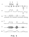
- FIG. 5 shows graphs to explain the operation at deteriorated reception performance.
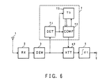
- FIG. 6 is a block diagram to show a first embodiment according to this invention (in particular, variable threshold and received signal attenuation).
- FIG. 7 shows waveforms of signals which explain removal of interference by the first embodiment.
- FIG. 8 shows the attenuation in relation to detected amount in deteriorated reception performance.
- FIG. 9 shows operation charts of the first embodiment.
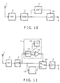
- FIG. 10 is a block diagram of another interference reduction circuit (fixed detection threshold and limitation of received signal envelopes).
- FIG. 11 is a block diagram of another embodiment of this invention (variable threshold and interpolation of received signals).
- FIG. 12 is a diagram to show an embodiment of the threshold generator which can vary threshold level.
- FIG. 13 is an explanatory view of operation to vary detection threshold.
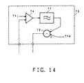
- FIG. 14 is a block diagram to show another embodiment of the threshold generator which can vary detection threshold.
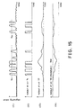
- FIG. 15 is an explanatory view of the operation to vary detection threshold.
- FIG. 16 is a block diagram of another embodiment of this invention (variable detection threshold, disconnection of received signals and received signal delay).
- FIG. 17 is an explanatory view of the embodiment of Fig. 16.
- FIG. 18 is a block diagram of another embodiment of this invention (digital signals, fixed detection threshold and error correction of received signals).
- FIG. 19 is an explanatory view of signal arrangement in the embodiment of Fig. 18.
- FIG. 20 is a block diagram of another interference reduction circuit (digital speech signals, fixed detection threshold and disconnection of received signals).
- FIG. 21 is a block diagram of another interference reduction circuit (diversity system).
- FIG. 22 is a block diagram of another interference reduction circuit (modified diversity system).
- FIG. 23 is a block diagram of another interference reduction circuit (modified diversity system).
- FIG. 24 is a diagram to show a logical circuit included in the circuit of Fig. 23.
- FIG. 25 is an explanatory view to show an improvement in quality of demodulated signals according to this invention.
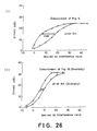
- FIG. 26 is a view to show the result of experiments which demonstrates the improvement in SINAD of received signals according to this invention.
- FIG. 3 is a block diagram of an interference reduction circuit wherein an antenna 1 is connected to a receiver 2, and output of the receiver 2 is connected to an FM demodulator 3.
- the output of the FM demodulator 3 is fed to an integrator 5 via a switch 4, and the output therefrom is directed to an output terminal 6.
- This circuit is characterized in that a detection circuit 7 is provided at the output of the FM demodulator 3 for detection of deterioration of reception performance so as to control with the output therefrom the switch 4 provided on the path of received signals.
- the detector 7 comprises an amplitude detector 71 which inputs the signals branched out from the output of the demodulator 3 and detects amplitude of FM demodulated signals, a comparator 72 which compares the output from the dedetector 71 with a threshold, and a threshold generator 73.
- the amplitude detector 71 may have a structure shown in FIG. 4a so as to feed the FM demodulated signals to a low-pass filter 11a, and feed the output therefrom to a full-wave rectifier 12a in order to detect the absolute value of the amplitude.
- FIGS. 4b and 4c show modifications of the amplitude detector 71 which will be described in more detail hereinafter.
- Graphs in FIG. 5 describe the operation of a deteriorated performance detector 7.
- jump phenomenon is produced in the envelope of the FM demodulated signals as shown by the letters A, B, C and D in FIG. 5i. More particularly, as described in relation to FIG. 2, frequency jump is produced by alternation of desired waves with undesired waves while beat occurs due to interference.
- the jumps shown by the letters A through C in FIG. 5i are caused by the interference from the upper side channel while those shown by the letter D is caused by the interference from the lower side channel.
- signals are removed of beat components to assume the waveforms shown in FIG. 5ii.
- 5iii is obtained by passing the above signals through a full-wave rectifier 12a.
- the comparator 72 detects that the output increases beyond a threshold Th, it judges that there is interference to output signals of FIG. 5iv from the detector 7.
- the switch 4 is turned off to disconnect the received signals. This operation prevents output of noise at high level to eliminate jarring noise.
- the Radio Law provides that the frequency deviation should be limited at a specific value or less on the transmitter side of a mobile radio communication system with analogue FM by an IDC circuit in order to prevent interference with other channels. Therefore, the threshold is preferably set at a level which can judge deviation higher than the regulated value as the interference.
- FIGS. 4b and 4c show modifications of the detector 71.
- FIG. 4b shows a detector which feeds FM demodulated signals to a band-pass filter 11b and detects the power level thereof.
- the beat shown in FIG. 5v is outputted.
- the beat frequency corresponds to the difference between the desired and undesired signals in frequency. For instance, if the channel interval is assumed to be 8 kHz, the beat will have the frequency around 8 kHz.
- the beat is fed to the full-wave rectifier 12b and smoothed by a low-pass filter 13b to output the beat power as shown in FIG. 5 vi.
- the deterioration in performance could be detected by an increase of the power beyond the threshold.
- the circuit of Fig.4b may be valid only when the duration of time at which the undesired signal dominates the desired signal is small enough. This is because the beat will not be in the demodulated signals in the midst of the duration, at which the undesired signal is much higher than the desired signal.
- the circuit shown in FIG. 4c is a detector which detects time derivative value of FM demodulated signals in the absolute values.
- FM demodulated signals drastically change to vary the amplitude chronologically.
- the FM demodulated signals are differentiated in time by the differentiator 11c, and its amplitude is obtained in absolute value by the full-wave rectifier 12c.
- the amplitude is temporarily held by a peak holding circuit 13c, and if the output therefrom increases beyond a threshold, the reception performance is judged deteriorated.
- the circuit shown in FIG. 4b or 4c is the circuit having better characteristics in utility than that shown in FIG. 4a.
- FIG. 6 is a block diagram to show the first embodiment of this invention.
- the first embodiment is characterized in that a variable attenuator 42 is provided on the path of the received signals in the FM demodulator 3 instead of the switch, and an additional circuit is provided to vary the threshold Th for detecting the reception performance depending on the received signals. More particularly, the variable attenuator 42 is inserted in the output of the FM demodulator 3, and the attenuation level is controlled by the output from the detector 7.
- the threshold generator 73 of the detector 7 is adapted to change the threshold depending on the output from the amplitude detector 71.
- Other structure is basically the same as the structure of Fig. 3, and description is omitted to avoid redundancy.
- the threshold generator 73 and the comparator 72 comprise microprocessors.
- the threshold generator 73 counts frequency of the output signals which is higher than the threshold in a predetermined period, and when the counted value exceeds a predetermined value, the threshold to be given to the comparator 72 is varied to a threshold Th' which is smaller than the above mentioned threshold Th.
- FIG. 7i the output signals from the FM demodulator 3 are marked with solid lines. Large noises are produced at times denoted by the letters A through F due to the interference from adjacent channels. Unless suitably removed, all of these noises will be outputted to greatly affect and deteriorate the speech quality.
- FIG. 7ii shows an application of this invention to such a case when the absolute value of FM demodulated signal increases beyond a predetermined threshold Th, a large attenuation is generated by the variable attenuator 42 so as to lower the level of the signals passing therethrough. This can remove large noises to a certain extent.
- threshold Th such as those shown by the letters C, E and F in FIG. 7i. Even if they reach the level, it might take longer to reach the threshold level. In other words, in such a case, noise cannot be removed completely but remains as shown in FIG. 7ii.
- the threshold should be set at a low enough value, but if it is set at too low a value, modulated signals of desired signals would be disconnected to distort signals and deteriorate speech quality even when there is no interference from adjacent channels.
- FIG. 7iii shows an operation when the threshold Th is varied to a smaller threshold Th ⁇ depending on the conditions. For instance, when interference occurs from an adjacent channel, and FM demodulated signals frequently go beyond the threshold Th, the threshold Th is changed to the threshold Th ⁇ . This removes practically all the noise shown in the right side of FIG. 7iii. Conversely, when the receiver condition is excellent substantially without interference, a higher threshold Th may be set and no demodulator output of desired signals is cut off. Under a condition where interference frequently occurs, even if the threshold is set low, modulated signals may be prevented. But even if it increases distortion, removal of interference noise will improve quality more remarkably to achieve an excellent speech quality.
- the method to vary the threshold is not limited to the above, but may be added with other factors such as fading pitch or change of desired signals to achieve higher effect.
- the threshold is varied periodically irrespective of the reception conditions.
- the levels of threshold are not limited to two, i.e. a high level and a low level, but may be three or more or can be varied continuously.
- threshold When data is transmitted with tone signals instead of speech signals, it is preferable to switch threshold automatically or manually from the ordinary analogue speech transmission type to a threshold of different type. If signals are cut with a threshold smaller than the maximum frequency deviation in MODEM signals, signals would not be transmitted correctly because of waveform distortion Therefore, for the MODEM signals, the threshold level should not be lower than the maximum frequency deviation.
- variable attenuator 42 The operation to attenuate received signals by means of a variable attenuator 42 instead of a mere disconnection by means of a switch and the relation thereof with threshold change will be described below.
- Figs. 8i and 8ii are charts to describe control characteristics of a variable attenuator 42 of the detector 7.
- the degree of deterioration in reception performance detected by the detector 7 is plotted on the horizontal axis while responsive attenuation by the attenuator 42 is plotted on the vertical axis.
- three values are set as thresholds, and when the degree of deterioration in performance reaches the thresholds Tha, Thb and Thc respectively, the attenuation by the attenuator 42 is controlled to reach infinity to block the passage of the signals.
- one threshold is selected out of three to present different control characteristics.
- Fig. 8ii shows a case where attenuation changes gradually depending on the degree of deterioration in reception performance.
- control charactereistics A, B and C are prepared in advance so that one out of three is selected for use. There is used no concept of threshold in the case shown in Fig. 8ii. When attenuation is varied continuously as in the case shown in Fig. 8ii, the circuit structure becomes complicated, but it can adjust attenuation depending on the degree of deterioration in performance to minimize the information lost by attenuation.
- Fig. 9 shows another method to control the variable attenuator 42 depending on the output from the detector 7.
- the method uses both the circuits a and b described in Fig. 4 as the amplitude detector 71, and it offers better performance.
- Solid line in Fig. 9(a) shows FM demodulator output, and dotted line is the beat power level.
- Th1 is the threshold of the detection circuit of Fig. 4(a)
- Th2 is that of the circuit of Fig. 4(b).
- a case where the characteristics of an attenuator 42 are those shown in Fig. 8i is taken for an example.
- the circuit of Fig. 4(a) is effective to detect the interference or undesired signal which becomes to dominate over the desired signal. However, it cannot detect the state immediately preceding the change. It is also defective in that it unavoidably outputs a detection output when it detects clicking noise due to co-channel interference.
- the circuit of Fig. 4(b) can detect interference before it becomes dominant over the desired signal, as shown in Fig. 5(v). But after the interference dominates, the detection output becomes small. As shown in Fig. 9, therefore, when attenuation is controlled by both circuits shown in Figs.
- Attenuation can be obtained even before the reversal of dominance and attenuation is secured at the time of reversal.
- the threshold Th1 and the threshold Th2 are set separately and respectively for the circuit in Fig. 4a and the one in Fig. 4b.
- the method of Fig. 9 can reduce residual noises.
- Fig. 10 is a block diagram of another interference reduction circuit.
- An amplitude limiter 41 is inserted in the output signal path of the FM demodulator 3, and the limiting level of the limiter 41 is controlled by the output from the deteriorated performance detector 7. More particularly, when the reception is detected to have deteriorated the limiting level of the amplitude limiter 41 is lowered so as to suppress the level of the noises passing therethrough.
- several threshold levels may be set, and the limiting level can be changed depending on the degree of the deterioration so that noise otherwise caused by interference can be reduced to improve the speech quality.
- the third embodiment is most effective when applied to FM transmission.
- FIG. 11 is a block diagram of another embodiment of this invention.
- the threshold in this embodiment may be shifted between two levels, and a switch circuit 40 inserted in the path of the signals from the FM demodulator 3 is used not merely to disconnect the signals but also to connect the path with the output from a signal interpolation circuit 10 while the signals are blocked so as to interpolate the signals lost by disconnection.
- the first embodiment of the signal interpolation circuit 10 continues the waveform immediately preceding. Vowels are generally known as the repetition of certain waveforms. Therefore, the vowel portion in a speech can be fairly faithfully restored by continuing the waveform of the signal immediately before the disconnection.
- the second embodiment interpolation circuit 10 can carry out more sophisticated interpolation by reproducing the waveform of one pitch immediately before the shifting of the switch 40 in a pitch aligned with interpolated portion.
- Such technology is described in detail in the paper entitled Time Diversity by Pitch-Synchronized Interpolation: IEEE Transaction Vehicular Technology VT-29 No. 4, 1980. It was proven that this technology can restore the data,which was once lost,due to the redundancy of speech to thereby remarkably improve the quality.
- FIG. 12 is a structural view to show a simply constructed threshold generator 73 wherein one of the inputs of the comparator is fed with a predetermined threshold Th1 while the other input is fed with the output from the amplitude detector 71.
- the comparator 74 is connected to a multi-vibrator 75 and generates output when the output from the detector 71 exceeds the threshold Th1.
- the output from the detector 71 has become lower than the threshold Th1, and a predetermined time T has elapsed, the output from the multi-vibrator 75 is suspended.
- One of the two levels of the threshold can be selected in supply to the comparator 72 by switching the switch 76 between the two thresholds of the higher one Th1 and the lower one Th2 in accordance with the output from the multi-vibrator 75.
- FIG. 13i is a chart to explain the operation to set a threshold by the circuit.
- the switch 76 switches between the higher threshold Th1 and the lower threshold Th2 for output.
- FIG. 13ii shows the waveforms after the FM demodulated signals have passed through the switch 40.
- the broken lines express the waveforms when the threshold Th1 is fixed wherein noise remains as the detected value is lower than the level Th1.
- FIG. 13i shows that these noises are almost removed when the threshold level is shifted.
- This embodiment is advantageous in that it can be constructed with simple circuits and is highly adaptive to various conditions as threshold therein is variable by switching.
- FIG. 14 is an explanatory view to show still another embodiment of the threshold generator 73.
- the output from the comparator 74 is passed through a low-pass filter 77, and the output therefrom is subtracted from the predetermined threshold Th ⁇ by a subtractor 78.
- FIG. 15 is an explanatory view of the operation to set the threshold by this circuit.
- FIG. 15i shows the output from the amplitude detector while
- FIG. 15ii shows the signals which passed a comparator 74 which compares the output from the detector with the threshold Th1.
- FIG. 15iii shows the signals which have passed through a low-pass filter 77.
- the signals are subtracted from the reference value Th ⁇ to obtain the threshold output shown in FIG. 15iv.
- the threshold can be lowered when the deterioration in reception performance is large in average, and noise can effectively be removed.
- FIG. 16 is a block diagram of another embodiment of this invention wherein a delay circuit 25 is inserted in the output signal path of the FM demodulator 3, the detector 7 has a variable threshold, and a switch 4 disconnects signals without interpolation.
- a delay is given to the FM demodulated signals, and the pulse width of the detector 71 output is extended by a pulse width transformer 20.
- Fig. 17 explains the operation thereof.
- Fig. 17i shows the output waveform from the amplitude detector 71
- Fig. 17ii the output waveform from the pulse width transformer 20
- Fig. 17iii the output waveform from the switch 4.
- the timing to cut off the signals with the switch 4 is relatively fast on the time axis of the FM demodulated signals, and the time duration of such disconnection is extended. This enables the noises caused by the interference from adjacent channels to be removed at an appropriate timing over a broader scope.
- Fig. 17ii the broken line represents inputs to the switch 4 that will appear it otherwise circuit is used.
- the solid line represents the corresponding inputs to the switch for this embodiment.
- the pulse width is increased on both sides by ⁇ respectively that is caused by delay circuit 25 and pulse width transformer 20.
- the demodulated signals are first delayed, and then controlled by switching.
- This method in general, is effective when the control is carried out on the basis of average deterioration over a given time. This is because it can adjust timing differences between control signals and demodulated signals to be controlled by it, even if the control signals are subjected to delay due to averaging process (e.g., in the embodiment shown in Fig. 14 a delay is caused by the low-pass filter).
- Fig. 18 is a block diagram to show another embodiment of this invention when applied to digital signal transmission.
- This embodiment circuit can correct errors in digital signals with the signal which detects the deterioration in reception performance.
- the received signals are the signals which have been modulated in angle with digital signals, and demodulated signals are obtained at the output of the FM demodulator 3.
- the digital signals are constructed in the unit of a frame and each frame has an error detection code.
- the output from the FM demodulator is branched out so as to detect the presence/absence of interference from adjacent channels by the detector 7. This is similar to the one described in relation to FIG. 3.
- the output signals from the FM demodulator 3 are discriminated by a discriminator 51 and inputted successively at a shift register 52.
- the output read out in serial from the shift register 52 is transmitted to an output terminal 54 via an exclusive OR 53.
- the error detecting circuit 56 detects errors in the unit of a frame, and when an error is detected, a flip-flop 57 is set at a high level.
- the deterioration in reception performance is detected in synchronization with the digital signals in the unit of a bit.
- the result of the detection is inputted at a shift register 61 bit by bit.
- the serial output from the shift register 61 is synchronized with the reading out of the received signals from the shift register 52.
- a timing controller 59 detects frame synchronizing signals with the output signals from a terminal 54, and a flip-flop 57 and a counter 62 are reset with the detection output in the unit of a frame.
- a counter 62 is a circuit which counts the bits of performance deterioration sent to the output of the shift register 61, and when the number of counted bits is large (e.g. two or higher) in one frame, the data about the frame is judged not reliable, and a signal to dispose the data of the frame is transmitted to a terminal 63.
- FIG. 19 is a chart to show trains of coded digital signals used in this embodiment wherein axx indicates a data bit, and cx a corresponding check bit. In this embodiment, even parity check is used as the check bits.
- the case shown in FIG. 19a is the one where the units of error correction are concentrated timewise while the case of FIG. 19b is the one where the units of error correction is decentralized timewise. They are both well known code trains, but the one shown in FIG. 19b is more suitable to the transmission paths where errors are likely to occur for more than two successive bits.
- This embodiment can detect whether error(s) is in the frame or not by means of the error detection capability and can identify the bit(s) which are most likely to have errors. As a result it can enhance error correcting capabilities.
- the concept can be applied to error correction over a still broader scope. For instance, if coding scheme that is capable of detecting N-bit errors but unable of error correction are used, errors on N bits can be corrected by this method.
- FIG. 20 is a block diagram of another interference reduction circuit which is applied to speech signals that have been digital-modulated.
- This circuit is a system which converts speech into digital signals for radio transmission, and the digital signals obtained at the output of the FM demodulator 3 are discriminated by a discriminator 51 and inputted at a speech decoder 62.
- the digital signals are decoded by the speech decoder 62.
- the signals which have detected deterioration in reception performance are delayed by the delay circuit 61 by the time required for the discriminator 51 and the speech decoder 62.
- the output signals from the decoder 62 are transmitted to an output terminal 64.
- the switch 63 is usually connected to a contact on the upper side, but when an output is transmitted from the delay circuit 61, the terminal 64 is grounded to make the output at the terminal 64 mute. Even if large noises are generated by interference and transmitted to the ouptut at the decoder 62, this construction can block out the noises to secure speech signals with a high legibility and quality.
- the part marked with broken lines in FIG. 20 may be realized by signal processing of the speech decoder, and error correction method shown in FIG. 18 may be used in parallel to the above in the processing. A further improvement can be achieved if the circuit is adapted to make the decision for mute period with the bit which detects interference from adjacent channels within a unit of correction (i.e. delete indicate 63 in FIG.18).
- FIG. 21 is a block diagram of an interference reduction circuit applied to a diversity receiver.
- judgement of whether or not the detected deterioration in reception performance exceeds a threshold is used for diversity branch selection algorithm.
- FIG. 21 there are provided two receiver systems each of which comprises an antenna 1, a receiver circuit 2, an FM demodulator 3 and a detector for deteriorated reception performance 7.
- FM demodulated signals are inputted at an integrator 5 via a switch 40 and the output therefrom is the output of the receiver 6.
- the selection control signals for control of the switch 40 are generated from a logical circuit 22.
- the circuit 22 receives,as inputs the outputs both from the detectors 7 of the two systems and from the comparator 21.
- the comparators 21 input signals l1 and l2 which represent the received amplitude obtained by the receiving circuits 2 of the two systems. To the output of the comparator 21 are transmitted the signals which indicate which of the signals l1 or l2 is larger.
- the switch 40 is controlled to select the output signals from the other receiving system.
- the switch 40 is controlled to select the output from the receiving system having a larger amplitude in accordance with the output from the comparator 21. This enables avoiding the system where interference occurs from adjacent channels, so that a diversity receiver system can be realized to achieve greater improvement not only in the prevention of thermal noises but also of interference from adjacent channels. (When the threshold is controlled to achieve the maximum effect, an even greater improvement may be attained.)
- FIG. 22 is a block diagram of an interference reduction circuit for a modification of the application
- This circuit can disconnect the demodulated signals from both of the receiving systems if interference occurs due to adjacent channels in both of the systems. More particularly, an amplitude detector 23 is provided at the output of the switch 40, and the output thereof is compared by the comparator 24 with the threshold generated by the generator 73. When the output from the detector 23 is larger, the switch 27 is turned off. Other structures are identical to those shown in relation to the seventh embodiment. When interference occurs from adjacent channels, received output is blocked off in the two receiving systems.
- a threshold generator is shared by the two receiving systems. This structure is effective in simplifying circuits when using a complicated circuit for the generator.
- FIG. 23 is a block diagram of another interference reduction circuit applied to diversity receiver systems.
- this circuit when interference occurs due to adjacent channels in both of the systems simultaneously, the received output is disconnected, and at the same time the systems are alternated in a given cycle so that the output can be selected from the proper system as soon as the interference disappears from the system.
- the logical circuit 30 in FIG. 23 is structured to judge which system should be selected from the output of the comparator 21 (or the relation between the levels of received signals) and the output from the detector 7 (or the result of the performance detection of the signals after switching) and to control the switch 40.
- FIG. 24 is a block diagram to show an example of the structure of the logical circuit 30 wherein the reference numeral 301 denotes a gate circuit, 302 and 303 mono-stable multi-vibrators, 304 a D flip-flop, and 305 and 306 a tristate buffer.
- the input/output lines H, I, J correspond to those in FIG. 23.
- the branch having a higher level of received signal envelopes is selected while when deterioration is detected in the signals after switching, it is switched to the output of the other system irrespective of the level of envelopes for a predetermined duration of time.
- branches are alternated in a predetermined cycle to seek for the system having no interference.
- FIG. 25 shows charts to explain about the improvement in the quality of demodulated signals by this operation.
- FIGS. 25i and 25ii show FM demodulated signals of the systems. Both show the waveform which has passed through a low-pass filter. At the position where undesired signals become dominant over the desired signals due to the interference from adjacent channels, a step-like change occurs.
- FIG. 25iii shows the output from the comparator 21 of FIG. 23 showing the relation between the received signal envelope levels. It becomes "High" when the level of the second system (2) is higher than the other. Based on FIG. 25iii, the first system (1) is selected, but the performance deteriorates at the time t1, and the system is switched forcibly to the second system (2) for the time duration,T1.
- T1 sec. After T1 sec., it again selects the first system, but as it still has performance deterioration, the system is further switched to the second system (2). At the time t2, as the second system also deteriorates in performance, branches should be alternated with each other at a time interval, T2.
- the switching signals for selection are shown in FIG. 25iv.
- FIG. 25v shows the result of deterioration detection after switching of signals. Based on FIGS. 25v and 25iii, the signals shown in FIG. 25iv are outputted. FIG. 25iv shows the output to disconnect the signals when deterioration occurs with the signals shown in FIG. 25v. It can select the receiving system having no interference, and at the same time block off the signals if deterioration occurs in both of the systems to prevent generation of large noises. This attains a remarkable improvement in quality.
- this embodiment uses one common detector 7 for both of the receiving systems, it greatly simplifies the circuit structure. This is most effective when a complicated circuit is employed to achieve highly precise detection of deteriorated performance.
- FIGS. 26i and 26ii are the graphs to show the improvement achieved experimentally by this invention in terms of ((signal + noise + distortion/(noise + distortion)) SINAD of received signals.
- the graph 26i shows the comparison in characteristics between the structure of this invention shown in FIG. 3 with the threshold setting circuit of FIG. 12 and a prior art. For instance, at the point 10dB of desired signal against undesired signal ratio, this invention improves SINAD by 10dB.
- the graph clearly shows that the ratio of desired wave against undesired wave which is required to make SINAD to 15dB can be reduced by 12dB from the prior art. This means that the interval between adjacent channels can be reduced remarkably. In other words, in a mobile communication system with a smaller zone, adjacent channels are set at a short interval which was heretofore impossible.
- FIG. 26ii shows an improvement achieved by the embodiment shown in FIG. 21 in SINAD of a diversity receiver. It is obvious from the graph that in addition to the improvement achieved generally by the diversity receiver, the ratio of desired wave against undesired wave required to increase SIAND to 15dB can be reduced by 3dB.
- this invention system can detect occurrence of interference due to adjacent channels from the absolute values of FM demodulated signals after they passed through a low-pass filter or from the electric power of the FM demodulated signals after they passed through the band-pass filter, control the signals at that time by disconnection, amplitude limiting or interpolation, and use the detection for the logic for selection of diversity branches to thereby reduce the deterioration in quality of the signals which might otherwise be caused by adjacent channel interference.
- This invention system can reduce large noises caused by the interference from adjacent channels.
- This system is further adaptive to reception conditions, and when deterioration is intensive, it can almost completely erase noises by allowing original signals to be disconnected more or less, thereby removing jarring noises and legible crosstalks. When performance is not deteriorated, the system can minimize the operation of disconnection to receive and reproduce the original signals faithfully.
- This invention system reduces interference noises flexibly in accordance with the receiving conditions to thereby remarkably enhance the speech quality.
Landscapes
- Physics & Mathematics (AREA)
- Electromagnetism (AREA)
- Engineering & Computer Science (AREA)
- Computer Networks & Wireless Communication (AREA)
- Signal Processing (AREA)
- Noise Elimination (AREA)
- Radio Transmission System (AREA)
Description
- This invention is applicable to mobile radio communications. This invention is applicable to reduction of interferences and noises in a receiver of radio signals which have been modulated in angle. More particularly, this invention is related to a technology which reduces noise otherwise caused by the interference from adjacent channels in a mobile radio communication system with interleaved channels which attempts to increase the efficiency in spectrum utilization by allowing overlap of radio frequency spectra.
- In mobile radio communication systems of FM, PM or other angle modulation systems, there are made attempts to minimize the frequency bandwidth occupied by one channel and maximize the number of channels usable in a given bandwidth to increase the efficiency in spectrum utilization. For this purpose, the technology to limit instantaneous frequency deviation within a predetermined scope in signal transmission is widely used.
- FIG. 1 is a diagram to show an embodiment of the signal transmission system structure of PM modulation wherein signals inputted at a
terminal 101 are differentiated by adifferentiator 102, limited in envelope by alimiter 103 within a predetermined scope of values, and then outputted from anantenna 106 via anFM modulator 104, and atransmitter 105. - In the receiving system, the signals are inputted through an
antenna 107, passed to areceiver 108, detected in frequency by afrequency discriminator 109 to be demodulated to FM demodulated signals, integrated by anintegrator 110, and then outputted from anoutput terminal 111. The modulated signal output can be maintained within a predetermined scope of maximum frequency deviation as the signals are modulated by theFM modulator 104 after they have been passed through thelimiter 103. - When interleaved channel arrangement is used to increase the spectrum utilization efficiency further, channels are arranged at a smaller frequency interval to allow overlapping of spectra between adjacent channels. FIG. 2 is a chart to show demodulated output when interference occurs in adjacent channels. In FIG. 2a, the solid line denotes fluctuation caused by fading entailed by the changes in the level of desired signals, while the broken line denotes fluctuation in levels of interfering signals from adjacent channels after they have passed through an IF filter in a receiver. The horizontal axis expresses time. As is obvious from FIG. 2a, there is a short time period when the level of undesired interfering signals is higher than that of desired signals. During this period undesired signals are demodulated by the capture effect in FM to appear in demodulated output. FM demodulated signals jumps in frequency during this period by the number of frequency equivalent to the frequency difference between adjacent channels to output the demodulated waveform shown in FIG. 2b. The graph represents the envelope of demodulated signals in vertical axis to indicate that the envelope corresponds to the frequency deviation before demodulation. The horizontal axis is the time axis with the same scale as FIG. 2a. FIG. 2b represents the signal waveform of the FM demodulated signals after they have passed through a low-pass filter, but for simplicity's sake, beat noise caused by interference is eliminated from the graph.
- Moreover, when interfering signals are modulated, the envelope thereof varies in accordance with the attenuation performance of an IF filter after the signals have passed the filter. When the level of interfering signals is high, the level of desired signals sometimes alternate with that of undesired signals at a pitch close to that of modulating signals in the undesired signals. In order to describe such a phenomenon, a part of FIG. 2b is enlarged in FIG. 2c.
- The amplitude of waveform shown in FIG. 2c corresponds to the frequency difference between adjacent channels, and more than twice of the maximum frequency deviation in modulated signals in conventional systems to cause noise of extremely large amplitude or energy level. Especially in speech communication systems using phase modulation, such waveforms are integrated to further emphasize the low frequency component thereof, producing quite jarring uncomfortable noises. The noises caused by the alternation between the level of desired signals and that of undesired signals due to the modulation of interfering signals becomes intelligible crosstalks to greatly affect the speech quality.
- As described above, the conventional systems are defective in that when adjacent channels interfer each other in signal levels in the arrangement of interleaved channels, even if the interfering signals are attenuated by an IF filter in a receiver, large noises proportional to the frequency difference between channels occur to thereby drastically deteriorate the signal-to-interference noise ratio performance of demodualated signals.
- One of the effective technologies to improve the receiver performance is called diversity reception. According to the technology, plural reception systems or diversity branches are provided so as to select signals of one of the branches or to synthesize plural signals for output from the system. In one of the well known technologies, received signal envelope levels of the plural systems are evaluated to select the output from the system having the higher envelope level. When the interference occurs between adjacent channels in such a receiver the branch having a higher level of adjacent channel interference is sometimes selected. The diversity technology is therefore not entirely free of the problems.
- British Patent Application No. 2 045 031 discloses a radio receiver including a signal processing path having a signal demodulator connected to pass its demodulated signals to signal conditioning means in the signal processing path, and an interference detection circuit connected to receive demodulated signals from the output terminal of the signal demodulator and to control the signal conditioning means according to the signal demodulator output. The interference detection circuit, as disclosed, includes a capacitor as an output element, the charge on the capacitor being indicative of the amount of interference detected by the interference detection circuit.
- European Patent Application No. 0 172 590 discloses a noise detector for detecting noise pulses in a non-limited incoming radio signal modulated on a carrier, comprising an amplitude detection circuit coupled to a first signal comparison arrangement having a signal input and a threshold input, a first threshold signal depending on the average input level of the noise detector and a second threshold signal depending on the noise pulse repetition frequency being applied to the threshold input, the threshold level of the noise detector being controlled in a forward direction in dependence on signal amplitude and the noise pulse repetition frequency.
- United States Patent No. 4 085 370 discloses an FM-radio receiver having an audio amplifier stage, provided with switching means, and a squelch circuit which is coupled to the output of the receiver demodulator, the squelch circuit comprising one circuit which produces an output signal rapidly when co-channel interference occurs and another circuit which produces an output signal which controls the switching means only when an impermissible signal/noise ratio and/or an impermissible degree of co-channel interference occurs.
- British Patent Application No. 2 073 551 discloses a noise blanking circuit including a noise detector amplifier arranged to detect noise impulses by differentiating an input signal containing noise impulses and amplifying the differentiated signal to produce an output comprising detected noise impulses, a noise blanking pulse generating circuit coupled to the output of the noise detection amplifier to produce blanking pulses in response to the magnitudes of the detected noise impulses present at the output and exceeding a predetermined threshold level, the noise blanking pulse generating circuit including rate shut-off circuitry allowing blanking pulses to be produced with a predetermined magnitude at the output only when the repetition rate of the detected noise pulses is below a selected maximum repetition rate, gating means coupled to the pulse generating circuit for receiving input signals and the blanking pulses and selectively passing or blocking input signals in response to the blanking pulses and control means coupled to the rate shut-off circuitry for blanking highly repetitive noise pulses.
- The invention provides a radio receiver capable of operation in an angle-modulated radio communication system employing a plurality of channels having frequency intervals so small that adjacent channels cause mutual interference in a receiver,
- the radio receiver including a signal processing path having a signal demodulator connected to pass its demodulated signals to signal conditioning means in the signal processing path, and an interference detection circuit connected to receive demodulated signals from the output terminal of the signal demodulator, the interference detection circuit being capable of generating an interference-controlling signal dependent on the demodulated signal it receives and being so connected to the signal conditioning means that, in operation, the interference-controlling signal controls the signal conditioning means, the interference detection circuit including a comparator having an output terminal that, in operation, provides the interference-controlling signal and applies it to the signal conditioning means, a threshold voltage source connected to a first input terminal of the comparator and a detector with its output terminal connected to a second input terminal of the comparator, the input terminal of the detector being connected to the output terminal of the signal demodulator, characterised in that the threshold voltage source includes means capable of selecting signals exceeding a first threshold from the detector, means capable of forming an average value of the selected signals and means capable of generating an output which is the difference between the average value and a second threshold.
- In a first arrangement, the detector includes an input bandwidth-limiting circuit capable of low-pass filtering connected in series with a first rectifying circuit.
- In a second arrangement, the detector includes an input bandwidth-limiting circuit capable of bandpass filtering connected in series with a second rectifying circuit and with a third bandwidth-limiting circuit capable of low-pass filtering.
- In a third arrangement, the detector includes an input bandwidth-limiting circuit capable of differentiation connected in series with a third rectifying circuit and with a peak voltage detection circuit.
- Preferably, the output terminal of the detector is connected to a control input terminal of the threshold voltage source for varying the output of the threshold voltage source in accordance with the output of the detector.
- In one arrangement, the threshold voltage source includes means capable of selecting one of a plurality of threshold voltages as its output.
- Preferably, the comparator is connected to the signal conditioning means by way of a pulse width adjusting circuit capable of adjusting the positions of control pulses relative to the controlling demodulated signals.
- In one arrangement, the radio receiver is a radio receiver capable of operation with digital signals and includes error-correcting means which, in operation, performs error correction at times when interference is being detected.
- In another arrangement, the radio receiver includes means for receiving a plurality of angle-modulated signals at the same time, means for determining the quality of each angle-modulated signal following its detection, and means for delivering a selected one of the angle-modulated signals along an output route after demodulation of the selected angle-modulated signal, wherein the means for determining the quality of each angle-modulated signal includes first comparison means for comparing the envelope sizes of the signals with a selected threshold and second comparison means for comparing the envelope sizes of the signals with one another, the means for delivering the selected signal along the output route including a logic circuit that selects the largest signal that does not, at the same time, exceed the selected threshold.
- The invention will now be described, by way of example only, with reference to the accompanying drawings.
- The circuits shown in Figs. 3, 10 and 20 to 23 are not embodiments of the invention and are included to assist in the understanding of the embodiments of the invention.
- FIG. 1 shows the structure of a signal transmission system in a phase-modulation system.
- FIG. 2 is an explanatory chart of frequency detection output when interference occurs between adjacent channels in an interleaved channel arrangement.
- FIG. 3 is a block diagram of an interference reduction circuit (in particular, fixed threshold to detect deteriorated reception performance, and disconnection of received signals).
- FIG. 4 is a chart to illustrate a structure of an envelope detection circuit.
- FIG. 5 shows graphs to explain the operation at deteriorated reception performance.
- FIG. 6 is a block diagram to show a first embodiment according to this invention (in particular, variable threshold and received signal attenuation).
- FIG. 7 shows waveforms of signals which explain removal of interference by the first embodiment.
- FIG. 8 shows the attenuation in relation to detected amount in deteriorated reception performance.
- FIG. 9 shows operation charts of the first embodiment.
- FIG. 10 is a block diagram of another interference reduction circuit (fixed detection threshold and limitation of received signal envelopes).
- FIG. 11 is a block diagram of another embodiment of this invention (variable threshold and interpolation of received signals).
- FIG. 12 is a diagram to show an embodiment of the threshold generator which can vary threshold level.
- FIG. 13 is an explanatory view of operation to vary detection threshold.
- FIG. 14 is a block diagram to show another embodiment of the threshold generator which can vary detection threshold.
- FIG. 15 is an explanatory view of the operation to vary detection threshold.
- FIG. 16 is a block diagram of another embodiment of this invention (variable detection threshold, disconnection of received signals and received signal delay).
- FIG. 17 is an explanatory view of the embodiment of Fig. 16.
- FIG. 18 is a block diagram of another embodiment of this invention (digital signals, fixed detection threshold and error correction of received signals).
- FIG. 19 is an explanatory view of signal arrangement in the embodiment of Fig. 18.
- FIG. 20 is a block diagram of another interference reduction circuit (digital speech signals, fixed detection threshold and disconnection of received signals).
- FIG. 21 is a block diagram of another interference reduction circuit (diversity system).
- FIG. 22 is a block diagram of another interference reduction circuit (modified diversity system).
- FIG. 23 is a block diagram of another interference reduction circuit (modified diversity system).
- FIG. 24 is a diagram to show a logical circuit included in the circuit of Fig. 23.
- FIG. 25 is an explanatory view to show an improvement in quality of demodulated signals according to this invention.
- FIG. 26 is a view to show the result of experiments which demonstrates the improvement in SINAD of received signals according to this invention.
- FIG. 3 is a block diagram of an interference reduction circuit wherein an
antenna 1 is connected to areceiver 2, and output of thereceiver 2 is connected to anFM demodulator 3. The output of theFM demodulator 3 is fed to anintegrator 5 via aswitch 4, and the output therefrom is directed to anoutput terminal 6. This circuit is characterized in that adetection circuit 7 is provided at the output of theFM demodulator 3 for detection of deterioration of reception performance so as to control with the output therefrom theswitch 4 provided on the path of received signals. - The
detector 7 comprises anamplitude detector 71 which inputs the signals branched out from the output of thedemodulator 3 and detects amplitude of FM demodulated signals, acomparator 72 which compares the output from thededetector 71 with a threshold, and athreshold generator 73. Theamplitude detector 71 may have a structure shown in FIG. 4a so as to feed the FM demodulated signals to a low-pass filter 11a, and feed the output therefrom to a full-wave rectifier 12a in order to detect the absolute value of the amplitude. FIGS. 4b and 4c show modifications of theamplitude detector 71 which will be described in more detail hereinafter. - Graphs in FIG. 5 describe the operation of a deteriorated
performance detector 7. When signals interfere between adjacent channels, jump phenomenon is produced in the envelope of the FM demodulated signals as shown by the letters A, B, C and D in FIG. 5i. More particularly, as described in relation to FIG. 2, frequency jump is produced by alternation of desired waves with undesired waves while beat occurs due to interference. The jumps shown by the letters A through C in FIG. 5i are caused by the interference from the upper side channel while those shown by the letter D is caused by the interference from the lower side channel. After having passed the low-pass filter 11a shown in FIG. 4a, signals are removed of beat components to assume the waveforms shown in FIG. 5ii. The output shown in FIG. 5iii is obtained by passing the above signals through a full-wave rectifier 12a. When thecomparator 72 detects that the output increases beyond a threshold Th, it judges that there is interference to output signals of FIG. 5iv from thedetector 7. As the period when the signal is being raised indicates interference, theswitch 4 is turned off to disconnect the received signals. This operation prevents output of noise at high level to eliminate jarring noise. - The Radio Law provides that the frequency deviation should be limited at a specific value or less on the transmitter side of a mobile radio communication system with analogue FM by an IDC circuit in order to prevent interference with other channels. Therefore, the threshold is preferably set at a level which can judge deviation higher than the regulated value as the interference.
- FIGS. 4b and 4c show modifications of the
detector 71. FIG. 4b shows a detector which feeds FM demodulated signals to a band-pass filter 11b and detects the power level thereof. When the signals of waveforms shown in FIG. 5i are passed through a band-pass filter 11b, the beat shown in FIG. 5v is outputted. In other words, the beat frequency corresponds to the difference between the desired and undesired signals in frequency. For instance, if the channel interval is assumed to be 8 kHz, the beat will have the frequency around 8 kHz. The beat is fed to the full-wave rectifier 12b and smoothed by a low-pass filter 13b to output the beat power as shown in FIG. 5 vi. The deterioration in performance could be detected by an increase of the power beyond the threshold. The circuit of Fig.4b, however, may be valid only when the duration of time at which the undesired signal dominates the desired signal is small enough. This is because the beat will not be in the demodulated signals in the midst of the duration, at which the undesired signal is much higher than the desired signal. - The circuit shown in FIG. 4c is a detector which detects time derivative value of FM demodulated signals in the absolute values. As shown in FIG. 5i, where interference occurs at A, B, C and D, FM demodulated signals drastically change to vary the amplitude chronologically. The FM demodulated signals are differentiated in time by the
differentiator 11c, and its amplitude is obtained in absolute value by the full-wave rectifier 12c. The amplitude is temporarily held by a peak holding circuit 13c, and if the output therefrom increases beyond a threshold, the reception performance is judged deteriorated. The circuit shown in FIG. 4b or 4c is the circuit having better characteristics in utility than that shown in FIG. 4a. - FIG. 6 is a block diagram to show the first embodiment of this invention. Compared to the circuit of Fig. 3, the first embodiment is characterized in that a
variable attenuator 42 is provided on the path of the received signals in theFM demodulator 3 instead of the switch, and an additional circuit is provided to vary the threshold Th for detecting the reception performance depending on the received signals. More particularly, thevariable attenuator 42 is inserted in the output of theFM demodulator 3, and the attenuation level is controlled by the output from thedetector 7. Thethreshold generator 73 of thedetector 7 is adapted to change the threshold depending on the output from theamplitude detector 71. Other structure is basically the same as the structure of Fig. 3, and description is omitted to avoid redundancy. - By providing a
variable attenuator 42 in place of a switch on the path of the received signals, it becomes more convenient as the receiver output does not become mute but is lowered to the degree as low as not to cause discomfort to the ears. Noises can be removed more effectively by setting a threshold Th variably in an optimal way to detect deterioration in performance. In the embodiment shown in FIG. 6, thethreshold generator 73 and thecomparator 72 comprise microprocessors. Thethreshold generator 73 counts frequency of the output signals which is higher than the threshold in a predetermined period, and when the counted value exceeds a predetermined value, the threshold to be given to thecomparator 72 is varied to a threshold Th' which is smaller than the above mentioned threshold Th. This structure can effectively remove noises as is explained below referring to FIG. 7. - In FIG. 7i, the output signals from the
FM demodulator 3 are marked with solid lines. Large noises are produced at times denoted by the letters A through F due to the interference from adjacent channels. Unless suitably removed, all of these noises will be outputted to greatly affect and deteriorate the speech quality. FIG. 7ii shows an application of this invention to such a case when the absolute value of FM demodulated signal increases beyond a predetermined threshold Th, a large attenuation is generated by thevariable attenuator 42 so as to lower the level of the signals passing therethrough. This can remove large noises to a certain extent. However, due to the operating range limitation, the bandwidth limit and influence of thermal noises, frequency jumps do not always reach the level of threshold Th such as those shown by the letters C, E and F in FIG. 7i. Even if they reach the level, it might take longer to reach the threshold level. In other words, in such a case, noise cannot be removed completely but remains as shown in FIG. 7ii. In order to fully remove the noises, the threshold should be set at a low enough value, but if it is set at too low a value, modulated signals of desired signals would be disconnected to distort signals and deteriorate speech quality even when there is no interference from adjacent channels. - FIG. 7iii shows an operation when the threshold Th is varied to a smaller threshold Thʹ depending on the conditions. For instance, when interference occurs from an adjacent channel, and FM demodulated signals frequently go beyond the threshold Th, the threshold Th is changed to the threshold Thʹ. This removes practically all the noise shown in the right side of FIG. 7iii. Conversely, when the receiver condition is excellent substantially without interference, a higher threshold Th may be set and no demodulator output of desired signals is cut off. Under a condition where interference frequently occurs, even if the threshold is set low, modulated signals may be prevented. But even if it increases distortion, removal of interference noise will improve quality more remarkably to achieve an excellent speech quality.
- The method to vary the threshold is not limited to the above, but may be added with other factors such as fading pitch or change of desired signals to achieve higher effect. Alternatively, the threshold is varied periodically irrespective of the reception conditions. The levels of threshold are not limited to two, i.e. a high level and a low level, but may be three or more or can be varied continuously.
- When data is transmitted with tone signals instead of speech signals, it is preferable to switch threshold automatically or manually from the ordinary analogue speech transmission type to a threshold of different type. If signals are cut with a threshold smaller than the maximum frequency deviation in MODEM signals, signals would not be transmitted correctly because of waveform distortion Therefore, for the MODEM signals, the threshold level should not be lower than the maximum frequency deviation.
- The operation to attenuate received signals by means of a
variable attenuator 42 instead of a mere disconnection by means of a switch and the relation thereof with threshold change will be described below. - Figs. 8i and 8ii are charts to describe control characteristics of a
variable attenuator 42 of thedetector 7. The degree of deterioration in reception performance detected by thedetector 7 is plotted on the horizontal axis while responsive attenuation by theattenuator 42 is plotted on the vertical axis. In Fig. 8i, three values are set as thresholds, and when the degree of deterioration in performance reaches the thresholds Tha, Thb and Thc respectively, the attenuation by theattenuator 42 is controlled to reach infinity to block the passage of the signals. Depending on the reception conditions, one threshold is selected out of three to present different control characteristics. Fig. 8ii shows a case where attenuation changes gradually depending on the degree of deterioration in reception performance. Three types of control charactereistics A, B and C are prepared in advance so that one out of three is selected for use. There is used no concept of threshold in the case shown in Fig. 8ii. When attenuation is varied continuously as in the case shown in Fig. 8ii, the circuit structure becomes complicated, but it can adjust attenuation depending on the degree of deterioration in performance to minimize the information lost by attenuation. - Fig. 9 shows another method to control the
variable attenuator 42 depending on the output from thedetector 7. The method uses both the circuits a and b described in Fig. 4 as theamplitude detector 71, and it offers better performance. Solid line in Fig. 9(a) shows FM demodulator output, and dotted line is the beat power level. Th₁ is the threshold of the detection circuit of Fig. 4(a), Th₂ is that of the circuit of Fig. 4(b). A case where the characteristics of anattenuator 42 are those shown in Fig. 8i is taken for an example. - As shown in Fig. 5(ii), the circuit of Fig. 4(a) is effective to detect the interference or undesired signal which becomes to dominate over the desired signal. However, it cannot detect the state immediately preceding the change. It is also defective in that it unavoidably outputs a detection output when it detects clicking noise due to co-channel interference. The circuit of Fig. 4(b), on the other hand, can detect interference before it becomes dominant over the desired signal, as shown in Fig. 5(v). But after the interference dominates, the detection output becomes small. As shown in Fig. 9, therefore, when attenuation is controlled by both circuits shown in Figs. 4a and 4b, attenuation can be obtained even before the reversal of dominance and attenuation is secured at the time of reversal. The threshold Th₁ and the threshold Th₂ are set separately and respectively for the circuit in Fig. 4a and the one in Fig. 4b. Thus,the method of Fig. 9 can reduce residual noises.
- Fig. 10 is a block diagram of another interference reduction circuit. An
amplitude limiter 41 is inserted in the output signal path of theFM demodulator 3, and the limiting level of thelimiter 41 is controlled by the output from the deterioratedperformance detector 7. More particularly, when the reception is detected to have deteriorated the limiting level of theamplitude limiter 41 is lowered so as to suppress the level of the noises passing therethrough. In this embodiment, several threshold levels may be set, and the limiting level can be changed depending on the degree of the deterioration so that noise otherwise caused by interference can be reduced to improve the speech quality. The third embodiment is most effective when applied to FM transmission. - FIG. 11 is a block diagram of another embodiment of this invention. The threshold in this embodiment may be shifted between two levels, and a
switch circuit 40 inserted in the path of the signals from theFM demodulator 3 is used not merely to disconnect the signals but also to connect the path with the output from asignal interpolation circuit 10 while the signals are blocked so as to interpolate the signals lost by disconnection. - The first embodiment of the
signal interpolation circuit 10 continues the waveform immediately preceding. Vowels are generally known as the repetition of certain waveforms. Therefore, the vowel portion in a speech can be fairly faithfully restored by continuing the waveform of the signal immediately before the disconnection. The secondembodiment interpolation circuit 10 can carry out more sophisticated interpolation by reproducing the waveform of one pitch immediately before the shifting of theswitch 40 in a pitch aligned with interpolated portion. Such technology is described in detail in the paper entitled Time Diversity by Pitch-Synchronized Interpolation: IEEE Transaction Vehicular Technology VT-29 No. 4, 1980. It was proven that this technology can restore the data,which was once lost,due to the redundancy of speech to thereby remarkably improve the quality. - FIG. 12 is a structural view to show a simply constructed
threshold generator 73 wherein one of the inputs of the comparator is fed with a predetermined threshold Th₁ while the other input is fed with the output from theamplitude detector 71. Thecomparator 74 is connected to a multi-vibrator 75 and generates output when the output from thedetector 71 exceeds the threshold Th₁. When the output from thedetector 71 has become lower than the threshold Th₁, and a predetermined time T has elapsed, the output from the multi-vibrator 75 is suspended. One of the two levels of the threshold can be selected in supply to thecomparator 72 by switching theswitch 76 between the two thresholds of the higher one Th₁ and the lower one Th₂ in accordance with the output from the multi-vibrator 75. FIG. 13i is a chart to explain the operation to set a threshold by the circuit. Theswitch 76 switches between the higher threshold Th₁ and the lower threshold Th₂ for output. FIG. 13ii shows the waveforms after the FM demodulated signals have passed through theswitch 40. In the chart, the broken lines express the waveforms when the threshold Th₁ is fixed wherein noise remains as the detected value is lower than the level Th₁. FIG. 13i shows that these noises are almost removed when the threshold level is shifted. This embodiment is advantageous in that it can be constructed with simple circuits and is highly adaptive to various conditions as threshold therein is variable by switching. - FIG. 14 is an explanatory view to show still another embodiment of the
threshold generator 73. In this embodiment the output from thecomparator 74 is passed through a low-pass filter 77, and the output therefrom is subtracted from the predetermined threshold Thø by asubtractor 78. FIG. 15 is an explanatory view of the operation to set the threshold by this circuit. FIG. 15i shows the output from the amplitude detector while FIG. 15ii shows the signals which passed acomparator 74 which compares the output from the detector with the threshold Th₁. FIG. 15iii shows the signals which have passed through a low-pass filter 77. The signals are subtracted from the reference value Thø to obtain the threshold output shown in FIG. 15iv. Thus the threshold can be lowered when the deterioration in reception performance is large in average, and noise can effectively be removed. - FIG. 16 is a block diagram of another embodiment of this invention wherein a
delay circuit 25 is inserted in the output signal path of theFM demodulator 3, thedetector 7 has a variable threshold, and aswitch 4 disconnects signals without interpolation. In the embodiment shown in Fig. 16 a delay is given to the FM demodulated signals, and the pulse width of thedetector 71 output is extended by apulse width transformer 20. Fig. 17 explains the operation thereof. Fig. 17i shows the output waveform from theamplitude detector 71, Fig. 17ii the output waveform from thepulse width transformer 20, and Fig. 17iii the output waveform from theswitch 4. In this structure, the timing to cut off the signals with theswitch 4 is relatively fast on the time axis of the FM demodulated signals, and the time duration of such disconnection is extended. This enables the noises caused by the interference from adjacent channels to be removed at an appropriate timing over a broader scope. - In Fig. 17ii, the broken line represents inputs to the
switch 4 that will appear it otherwise circuit is used. The solid line represents the corresponding inputs to the switch for this embodiment. The pulse width is increased on both sides by Δ respectively that is caused bydelay circuit 25 andpulse width transformer 20. - Further improvement is expected by adaptively controlling the changes in pulse width through the
transformer 20, according to the degree of deterioration. - In this embodiment, the demodulated signals are first delayed, and then controlled by switching. This method, in general, is effective when the control is carried out on the basis of average deterioration over a given time. This is because it can adjust timing differences between control signals and demodulated signals to be controlled by it, even if the control signals are subjected to delay due to averaging process (e.g., in the embodiment shown in Fig. 14 a delay is caused by the low-pass filter).
- Fig. 18 is a block diagram to show another embodiment of this invention when applied to digital signal transmission. This embodiment circuit can correct errors in digital signals with the signal which detects the deterioration in reception performance.
- In Fig. 18 the received signals are the signals which have been modulated in angle with digital signals, and demodulated signals are obtained at the output of the
FM demodulator 3. The digital signals are constructed in the unit of a frame and each frame has an error detection code. The output from the FM demodulator is branched out so as to detect the presence/absence of interference from adjacent channels by thedetector 7. This is similar to the one described in relation to FIG. 3. The output signals from theFM demodulator 3 are discriminated by adiscriminator 51 and inputted successively at a shift register 52. The output read out in serial from the shift register 52 is transmitted to an output terminal 54 via an exclusive OR 53. Theerror detecting circuit 56 detects errors in the unit of a frame, and when an error is detected, a flip-flop 57 is set at a high level. The deterioration in reception performance is detected in synchronization with the digital signals in the unit of a bit. The result of the detection is inputted at ashift register 61 bit by bit. The serial output from theshift register 61 is synchronized with the reading out of the received signals from the shift register 52. When an error is detected in one frame of received signals, and the flip-flop 57 is set at the high level, the bit which is detected for deterioration by theshift register 61 is likely to have an error. Therefore, an output is transmitted for the bit to an ANDcircuit 58 so that the output from the shift register 52 for the bit is inverted for correction by the exclusive OR 53. Atiming controller 59 detects frame synchronizing signals with the output signals from a terminal 54, and a flip-flop 57 and acounter 62 are reset with the detection output in the unit of a frame. Acounter 62 is a circuit which counts the bits of performance deterioration sent to the output of theshift register 61, and when the number of counted bits is large (e.g. two or higher) in one frame, the data about the frame is judged not reliable, and a signal to dispose the data of the frame is transmitted to a terminal 63. - FIG. 19 is a chart to show trains of coded digital signals used in this embodiment wherein axx indicates a data bit, and cx a corresponding check bit. In this embodiment, even parity check is used as the check bits. The case shown in FIG. 19a is the one where the units of error correction are concentrated timewise while the case of FIG. 19b is the one where the units of error correction is decentralized timewise. They are both well known code trains, but the one shown in FIG. 19b is more suitable to the transmission paths where errors are likely to occur for more than two successive bits.
- This embodiment can detect whether error(s) is in the frame or not by means of the error detection capability and can identify the bit(s) which are most likely to have errors. As a result it can enhance error correcting capabilities.
- The concept can be applied to error correction over a still broader scope. For instance, if coding scheme that is capable of detecting N-bit errors but unable of error correction are used, errors on N bits can be corrected by this method.
- FIG. 20 is a block diagram of another interference reduction circuit which is applied to speech signals that have been digital-modulated. This circuit is a system which converts speech into digital signals for radio transmission, and the digital signals obtained at the output of the
FM demodulator 3 are discriminated by adiscriminator 51 and inputted at aspeech decoder 62. The digital signals are decoded by thespeech decoder 62. The signals which have detected deterioration in reception performance are delayed by thedelay circuit 61 by the time required for thediscriminator 51 and thespeech decoder 62. The output signals from thedecoder 62 are transmitted to anoutput terminal 64. Theswitch 63 is usually connected to a contact on the upper side, but when an output is transmitted from thedelay circuit 61, the terminal 64 is grounded to make the output at the terminal 64 mute. Even if large noises are generated by interference and transmitted to the ouptut at thedecoder 62, this construction can block out the noises to secure speech signals with a high legibility and quality. The part marked with broken lines in FIG. 20 may be realized by signal processing of the speech decoder, and error correction method shown in FIG. 18 may be used in parallel to the above in the processing. A further improvement can be achieved if the circuit is adapted to make the decision for mute period with the bit which detects interference from adjacent channels within a unit of correction (i.e. delete indicate 63 in FIG.18). - An application of interference reduction circuits to a diversity receiver will now be described.
- FIG. 21 is a block diagram of an interference reduction circuit applied to a diversity receiver. In this diversity method, judgement of whether or not the detected deterioration in reception performance exceeds a threshold is used for diversity branch selection algorithm.
- In FIG. 21, there are provided two receiver systems each of which comprises an
antenna 1, areceiver circuit 2, anFM demodulator 3 and a detector for deterioratedreception performance 7. FM demodulated signals are inputted at anintegrator 5 via aswitch 40 and the output therefrom is the output of thereceiver 6. The selection control signals for control of theswitch 40 are generated from alogical circuit 22. Thecircuit 22 receives,as inputs the outputs both from thedetectors 7 of the two systems and from thecomparator 21. Thecomparators 21 input signals ℓ₁ and ℓ₂ which represent the received amplitude obtained by the receivingcircuits 2 of the two systems. To the output of thecomparator 21 are transmitted the signals which indicate which of the signals ℓ₁ or ℓ₂ is larger. - In the
logical circuit 22, while thedetector 7 of the one system is transmitting the signals indicating the performance deterioration, theswitch 40 is controlled to select the output signals from the other receiving system. When both of or none of receiving systems output signals of performance deterioration, theswitch 40 is controlled to select the output from the receiving system having a larger amplitude in accordance with the output from thecomparator 21. This enables avoiding the system where interference occurs from adjacent channels, so that a diversity receiver system can be realized to achieve greater improvement not only in the prevention of thermal noises but also of interference from adjacent channels. (When the threshold is controlled to achieve the maximum effect, an even greater improvement may be attained.) - FIG. 22 is a block diagram of an interference reduction circuit for a modification of the application
- to a diversity receiver system. This circuit can disconnect the demodulated signals from both of the receiving systems if interference occurs due to adjacent channels in both of the systems. More particularly, an
amplitude detector 23 is provided at the output of theswitch 40, and the output thereof is compared by thecomparator 24 with the threshold generated by thegenerator 73. When the output from thedetector 23 is larger, theswitch 27 is turned off. Other structures are identical to those shown in relation to the seventh embodiment. When interference occurs from adjacent channels, received output is blocked off in the two receiving systems. - In this circuit a threshold generator is shared by the two receiving systems. This structure is effective in simplifying circuits when using a complicated circuit for the generator.
- FIG. 23 is a block diagram of another interference reduction circuit applied to diversity receiver systems. In this circuit , when interference occurs due to adjacent channels in both of the systems simultaneously, the received output is disconnected, and at the same time the systems are alternated in a given cycle so that the output can be selected from the proper system as soon as the interference disappears from the system. The
logical circuit 30 in FIG. 23 is structured to judge which system should be selected from the output of the comparator 21 (or the relation between the levels of received signals) and the output from the detector 7 (or the result of the performance detection of the signals after switching) and to control theswitch 40. - FIG. 24 is a block diagram to show an example of the structure of the
logical circuit 30 wherein thereference numeral 301 denotes a gate circuit, 302 and 303 mono-stable multi-vibrators, 304 a D flip-flop, and 305 and 306 a tristate buffer. The input/output lines H, I, J correspond to those in FIG. 23. In this embodiment when no deterioration occurs in performance, the branch having a higher level of received signal envelopes is selected while when deterioration is detected in the signals after switching, it is switched to the output of the other system irrespective of the level of envelopes for a predetermined duration of time. When performance is being deteriorated also in the other system, branches are alternated in a predetermined cycle to seek for the system having no interference. - In the circuit shown in FIG. 24, when there is no H input (the result of deteriorated performance detection after signal switching), I input (relation of envelope levels) is passed through the
buffer 306 to become J output as it is. When there is H input, the mono-stable multi-vibrator 303 becomes "High" for a predetermined time, Ti sec, to make thebuffer 305 effective, and the output obtained by inverting the output before H input is outputted from Q output of the D flip-flop 304. If H input is still "High", the mono-stable multi-vibrator 302 repeated the inversion of the output from the D flip-flop 304 after a predetermined time T₂. - FIG. 25 shows charts to explain about the improvement in the quality of demodulated signals by this operation. FIGS. 25i and 25ii show FM demodulated signals of the systems. Both show the waveform which has passed through a low-pass filter. At the position where undesired signals become dominant over the desired signals due to the interference from adjacent channels, a step-like change occurs. FIG. 25iii shows the output from the
comparator 21 of FIG. 23 showing the relation between the received signal envelope levels. It becomes "High" when the level of the second system (2) is higher than the other. Based on FIG. 25iii, the first system (1) is selected, but the performance deteriorates at the time t₁, and the system is switched forcibly to the second system (2) for the time duration,T₁. After T₁ sec., it again selects the first system, but as it still has performance deterioration, the system is further switched to the second system (2). At the time t₂, as the second system also deteriorates in performance, branches should be alternated with each other at a time interval, T₂. The switching signals for selection are shown in FIG. 25iv. - FIG. 25v shows the result of deterioration detection after switching of signals. Based on FIGS. 25v and 25iii, the signals shown in FIG. 25iv are outputted. FIG. 25iv shows the output to disconnect the signals when deterioration occurs with the signals shown in FIG. 25v. It can select the receiving system having no interference, and at the same time block off the signals if deterioration occurs in both of the systems to prevent generation of large noises. This attains a remarkable improvement in quality.
- As this embodiment uses one
common detector 7 for both of the receiving systems, it greatly simplifies the circuit structure. This is most effective when a complicated circuit is employed to achieve highly precise detection of deteriorated performance. - FIGS. 26i and 26ii are the graphs to show the improvement achieved experimentally by this invention in terms of ((signal + noise + distortion/(noise + distortion)) SINAD of received signals. The graph 26i shows the comparison in characteristics between the structure of this invention shown in FIG. 3 with the threshold setting circuit of FIG. 12 and a prior art. For instance, at the point 10dB of desired signal against undesired signal ratio, this invention improves SINAD by 10dB.
- The graph clearly shows that the ratio of desired wave against undesired wave which is required to make SINAD to 15dB can be reduced by 12dB from the prior art. This means that the interval between adjacent channels can be reduced remarkably. In other words, in a mobile communication system with a smaller zone, adjacent channels are set at a short interval which was heretofore impossible.
- FIG. 26ii shows an improvement achieved by the embodiment shown in FIG. 21 in SINAD of a diversity receiver. It is obvious from the graph that in addition to the improvement achieved generally by the diversity receiver, the ratio of desired wave against undesired wave required to increase SIAND to 15dB can be reduced by 3dB.
- As described in the foregoing, this invention system can detect occurrence of interference due to adjacent channels from the absolute values of FM demodulated signals after they passed through a low-pass filter or from the electric power of the FM demodulated signals after they passed through the band-pass filter, control the signals at that time by disconnection, amplitude limiting or interpolation, and use the detection for the logic for selection of diversity branches to thereby reduce the deterioration in quality of the signals which might otherwise be caused by adjacent channel interference.
- This invention system can reduce large noises caused by the interference from adjacent channels. This system is further adaptive to reception conditions, and when deterioration is intensive, it can almost completely erase noises by allowing original signals to be disconnected more or less, thereby removing jarring noises and legible crosstalks. When performance is not deteriorated, the system can minimize the operation of disconnection to receive and reproduce the original signals faithfully. This invention system reduces interference noises flexibly in accordance with the receiving conditions to thereby remarkably enhance the speech quality.
- If the probability of interference is the same, application of this invention system can enhance the speech quality. Conversely, if the speech quality is constant, as this invention system realizes use of adjacent channels at a smaller frequency interval and within a shorter distance, the application of this invention system can realize a higher frequency efficiency.
Claims (9)
- A radio receiver capable of operation in an angle-modulated radio communication system employing a plurality of channels having frequency intervals so small that adjacent channels cause mutual interference in a receiver,the radio receiver including a signal processing path having a signal demodulator (3) connected to pass its demodulated signals to signal conditioning means (4) in the signal processing path, and an interference detection circuit (7) connected to receive demodulated signals from the output terminal of the signal demodulator (3), the interference detection circuit (7) being capable of generating an interference-controlling signal dependent on the demodulated signal it receives and being so connected to the signal conditioning means (4) that, in operation, the interference-controlling signal controls the signal conditioning means (4), the interference detection circuit (7) including a comparator (72) having an output terminal that, in operation, provides the interference-controlling signal and applies it to the signal conditioning means (4), a threshold voltage source (73) connected to a first input terminal of the comparator (72) and a detector (71) with its output terminal connected to a second input terminal of the comparator (72), the input terminal of the detector (71) being connected to the output terminal of the signal demodulator (3), characterised in thatthe threshold voltage source (73) includes means (74) capable of selecting signals exceeding a first threshold from the detector (71), means (77) capable of forming an average value of the selected signals and means (78) capable of generating an output which is the difference between the average value and a second threshold.
- A radio receiver as claimed in claim 1, wherein the detector (71) includes an input bandwidth-limiting circuit (11a) capable of low-pass filtering connected in series with a first rectifying circuit (12a).
- A radio receiver as claimed in claim 1, wherein the detector (71) includes an input bandwidth-limiting circuit (11b) capable of bandpass filtering connected in series with a second rectifying circuit (12b) and with a third bandwidth-limiting circuit (13b) capable of lowpass filtering.
- A radio receiver as claimed in claim 1, wherein the detector (71) includes an input bandwidth-limiting circuit (11c) capable of differentiation connected in series with a third rectifying circuit (12c) and with a peak voltage detection circuit (13c).
- A radio receiver as claimed in any one of claims 1 to 4, wherein the output terminal of the detector (71) is connected to a control input terminal of the threshold voltage source (73) for varying the output of the threshold voltage source (73) in accordance with the output of the detector (71).
- A radio receiver as claimed in claim 5, wherein the threshold voltage source (73) includes means (74,75,76) capable of selecting one of a plurality of threshold voltages as its output.
- A radio receiver as claimed in any one of claims 1 to 6, wherein the comparator (72) is connected to the signal conditioning means (4) by way of a pulse width adjusting circuit (20) capable of adjusting the positions of control pulses relative to the controlling demodulated signals.
- A radio receiver as claimed in any one of claims 1 to 7, capable of operation with digital signals, including error-correcting means (57,58,59,53) which, in operation, performs error correction at times when interference is being detected.
- A radio receiver as claimed in any one of claims 1 to 8, including means for receiving a plurality of angle-modulated signals at the same time, means (7,21) for determining the quality of each angle-modulated signal following its detection, and means (22,40) for delivering a selected one of the angle-modulated signals along an output route (5,6) after demodulation of the selected angle-modulated signal, wherein the means (7,21) for determining the quality of each angle-modulated signal includes first comparison means (7) for comparing the envelope sizes of the signals with a selected threshold and second comparison means (21) for comparing the envelope sizes of the signals with one another, the means (22,40) for delivering the selected signal along the output route (5,6) including a logic circuit (22) that selects the largest signal that does not, at the same time, exceed the selected threshold.
Applications Claiming Priority (4)
| Application Number | Priority Date | Filing Date | Title |
|---|---|---|---|
| JP63957/87 | 1987-03-20 | ||
| JP6395787A JPH0817334B2 (en) | 1987-03-20 | 1987-03-20 | Interference mitigation signal transmission method in mobile communication |
| JP165245/87 | 1987-07-03 | ||
| JP62165245A JPS6411429A (en) | 1987-07-03 | 1987-07-03 | Interference reduced signal transmission system for mobile communication |
Publications (3)
| Publication Number | Publication Date |
|---|---|
| EP0283299A2 EP0283299A2 (en) | 1988-09-21 |
| EP0283299A3 EP0283299A3 (en) | 1991-03-13 |
| EP0283299B1 true EP0283299B1 (en) | 1996-05-08 |
Family
ID=26405083
Family Applications (1)
| Application Number | Title | Priority Date | Filing Date |
|---|---|---|---|
| EP88302385A Expired - Lifetime EP0283299B1 (en) | 1987-03-20 | 1988-03-18 | Radio receiver |
Country Status (3)
| Country | Link |
|---|---|
| US (1) | US4969207A (en) |
| EP (1) | EP0283299B1 (en) |
| DE (1) | DE3855263T2 (en) |
Cited By (1)
| Publication number | Priority date | Publication date | Assignee | Title |
|---|---|---|---|---|
| US9749263B2 (en) | 2014-11-05 | 2017-08-29 | Motorola Solutions, Inc. | Methods and systems for identifying and reducing LTE-system coverage holes due to external interference |
Families Citing this family (44)
| Publication number | Priority date | Publication date | Assignee | Title |
|---|---|---|---|---|
| CA2052802A1 (en) * | 1990-10-11 | 1993-04-05 | Robert R. Clappier | Fm receiver anti-fading method and system |
| JP2760240B2 (en) * | 1992-03-11 | 1998-05-28 | 松下電器産業株式会社 | Noise suppression device |
| JP3218736B2 (en) * | 1992-11-06 | 2001-10-15 | ソニー株式会社 | Receivers and space diversity receivers |
| TW237587B (en) * | 1993-03-19 | 1995-01-01 | Philips Electronics Nv | |
| GB2281479B (en) * | 1993-08-27 | 1997-09-03 | Nokia Telecommunications Oy | Radio receiving apparatus |
| JPH0884104A (en) * | 1994-09-09 | 1996-03-26 | Toshiba Corp | Wireless communication device |
| FR2724519B1 (en) * | 1994-09-14 | 1996-12-13 | Sgs Thomson Microelectronics | TRANSMISSION PRESENCE DETECTOR IN A MODEM |
| US5603107A (en) * | 1995-06-09 | 1997-02-11 | Ford Motor Company | Switching system for diversity antenna FM receiver |
| JP3465434B2 (en) * | 1995-09-06 | 2003-11-10 | ソニー・プレシジョン・テクノロジー株式会社 | Laser doppler speedometer |
| JP3483695B2 (en) * | 1996-03-14 | 2004-01-06 | 株式会社リコー | Voice communication device |
| GB2352140B (en) * | 1996-06-10 | 2001-04-04 | Motorola As | A communications system |
| JP3154679B2 (en) * | 1996-10-18 | 2001-04-09 | 三菱電機株式会社 | Error correction decoding apparatus and decoding method for concatenated code |
| US5828699A (en) * | 1997-01-30 | 1998-10-27 | Harris Corporation | Automatic differential absolute time delay equalizer |
| JP3724940B2 (en) * | 1998-01-08 | 2005-12-07 | 株式会社東芝 | OFDM diversity receiver |
| US6445732B1 (en) * | 1998-09-23 | 2002-09-03 | Conexant Systems, Inc. | Dynamic range reduction circuitry for a digital communications receiver |
| EP0989559A1 (en) * | 1998-09-23 | 2000-03-29 | Deutsche Thomson-Brandt Gmbh | Disturbance detection in a data signal |
| US6862317B1 (en) * | 2000-07-25 | 2005-03-01 | Thomson Licensing S.A. | Modulation technique providing high data rate through band limited channels |
| DE10064493A1 (en) * | 2000-12-22 | 2002-06-27 | Bosch Gmbh Robert | Method for suppressing interference peaks in a useful signal |
| US6760551B2 (en) * | 2002-10-29 | 2004-07-06 | Agilent Technologies, Inc. | Adaptive decoder for skin effect limited signals |
| US7203471B2 (en) * | 2002-12-30 | 2007-04-10 | Motorola, Inc. | System and method for selectively utilizing an attenuation device in a two-way radio receiver based on squelch detect and radio signal strength indication (RSSI) |
| US9026070B2 (en) * | 2003-12-18 | 2015-05-05 | Qualcomm Incorporated | Low-power wireless diversity receiver with multiple receive paths |
| KR100608001B1 (en) * | 2004-08-17 | 2006-08-02 | 삼성전자주식회사 | Current limiting device and method of audio amplifier |
| US9450665B2 (en) | 2005-10-19 | 2016-09-20 | Qualcomm Incorporated | Diversity receiver for wireless communication |
| US7986928B2 (en) * | 2007-12-07 | 2011-07-26 | Motorola Mobility, Inc. | Method and apparatus for selecting a radio channel for transmitting an audio signal to a radio local receiver |
| US8385867B2 (en) * | 2009-06-29 | 2013-02-26 | Silicon Laboratories Inc. | Tracking filter for a television tuner |
| US9178669B2 (en) | 2011-05-17 | 2015-11-03 | Qualcomm Incorporated | Non-adjacent carrier aggregation architecture |
| US9252827B2 (en) | 2011-06-27 | 2016-02-02 | Qualcomm Incorporated | Signal splitting carrier aggregation receiver architecture |
| US9154179B2 (en) | 2011-06-29 | 2015-10-06 | Qualcomm Incorporated | Receiver with bypass mode for improved sensitivity |
| US12081243B2 (en) | 2011-08-16 | 2024-09-03 | Qualcomm Incorporated | Low noise amplifiers with combined outputs |
| US8774334B2 (en) | 2011-11-09 | 2014-07-08 | Qualcomm Incorporated | Dynamic receiver switching |
| US9362958B2 (en) | 2012-03-02 | 2016-06-07 | Qualcomm Incorporated | Single chip signal splitting carrier aggregation receiver architecture |
| US9172402B2 (en) | 2012-03-02 | 2015-10-27 | Qualcomm Incorporated | Multiple-input and multiple-output carrier aggregation receiver reuse architecture |
| US9118439B2 (en) | 2012-04-06 | 2015-08-25 | Qualcomm Incorporated | Receiver for imbalanced carriers |
| US9154356B2 (en) | 2012-05-25 | 2015-10-06 | Qualcomm Incorporated | Low noise amplifiers for carrier aggregation |
| US9867194B2 (en) | 2012-06-12 | 2018-01-09 | Qualcomm Incorporated | Dynamic UE scheduling with shared antenna and carrier aggregation |
| US9300420B2 (en) | 2012-09-11 | 2016-03-29 | Qualcomm Incorporated | Carrier aggregation receiver architecture |
| US9543903B2 (en) | 2012-10-22 | 2017-01-10 | Qualcomm Incorporated | Amplifiers with noise splitting |
| US8995591B2 (en) | 2013-03-14 | 2015-03-31 | Qualcomm, Incorporated | Reusing a single-chip carrier aggregation receiver to support non-cellular diversity |
| WO2015169379A1 (en) * | 2014-05-08 | 2015-11-12 | Epcos Ag | Circuit and method of operating a circuit |
| DE102014014449A1 (en) * | 2014-09-26 | 2016-03-31 | Giesecke & Devrient Gmbh | Method and security module for receiving two signals |
| US10177722B2 (en) | 2016-01-12 | 2019-01-08 | Qualcomm Incorporated | Carrier aggregation low-noise amplifier with tunable integrated power splitter |
| JP6812816B2 (en) * | 2017-02-03 | 2021-01-13 | 株式会社Jvcケンウッド | Receiver, receiving method, program |
| US10999102B1 (en) * | 2020-02-28 | 2021-05-04 | Nxp B.V. | FM spectrum estimation relative to adjacent channel |
| JP7541254B2 (en) * | 2020-12-28 | 2024-08-28 | 日本電信電話株式会社 | Optical transmitter and signal detection method |
Family Cites Families (10)
| Publication number | Priority date | Publication date | Assignee | Title |
|---|---|---|---|---|
| US3729682A (en) * | 1971-08-02 | 1973-04-24 | Gen Electric | Audio signal quality indicating circuit |
| NL163917C (en) * | 1975-10-02 | 1980-10-15 | Philips Nv | RADIO RECEIVER. |
| US4035729A (en) * | 1976-05-21 | 1977-07-12 | General Electric Company | Audio signal quality indicating circuit |
| US4154980A (en) * | 1977-08-29 | 1979-05-15 | Motorola, Inc. | Noise blanker with variable rate-shut-off and/or variable blanking threshold level |
| DE2909520C3 (en) * | 1979-03-10 | 1981-12-03 | Philips Patentverwaltung Gmbh, 2000 Hamburg | Circuit arrangement for attenuating background noises |
| DE3220429A1 (en) * | 1982-05-29 | 1983-12-01 | Blaupunkt-Werke Gmbh, 3200 Hildesheim | VHF stereo receiver with noise pulse blanking |
| US4539710A (en) * | 1983-09-30 | 1985-09-03 | Transkinetics Systems, Inc. | Diversity telemetry receiver having plural spaced antennas |
| JPS6077114U (en) * | 1983-11-01 | 1985-05-29 | パイオニア株式会社 | FM signal demodulator |
| GB2161344A (en) * | 1984-07-06 | 1986-01-08 | Philips Electronic Associated | Transmission of digital data |
| NL8402321A (en) * | 1984-07-23 | 1986-02-17 | Philips Nv | FAULT DETECTOR. |
-
1988
- 1988-03-17 US US07/169,501 patent/US4969207A/en not_active Expired - Fee Related
- 1988-03-18 DE DE3855263T patent/DE3855263T2/en not_active Expired - Fee Related
- 1988-03-18 EP EP88302385A patent/EP0283299B1/en not_active Expired - Lifetime
Cited By (1)
| Publication number | Priority date | Publication date | Assignee | Title |
|---|---|---|---|---|
| US9749263B2 (en) | 2014-11-05 | 2017-08-29 | Motorola Solutions, Inc. | Methods and systems for identifying and reducing LTE-system coverage holes due to external interference |
Also Published As
| Publication number | Publication date |
|---|---|
| EP0283299A3 (en) | 1991-03-13 |
| DE3855263D1 (en) | 1996-06-13 |
| DE3855263T2 (en) | 1997-01-09 |
| EP0283299A2 (en) | 1988-09-21 |
| US4969207A (en) | 1990-11-06 |
Similar Documents
| Publication | Publication Date | Title |
|---|---|---|
| US4969207A (en) | Radio receiver with reception deterioration compensation | |
| JP4727303B2 (en) | Mixed-mode adaptive analog reception architecture for data communication | |
| US5809065A (en) | Method and apparatus for improving the quality of AM compatible digital broadcast system signals in the presence of distortion | |
| CA1282126C (en) | Digital signal demodulation system | |
| CA2221317C (en) | Detection of co-channel interference in digital television signals | |
| US5553081A (en) | Apparatus and method for detecting a signal in a communications system | |
| KR100329673B1 (en) | Method and apparatus for DC offset clearing and automatic gain control in quadrature receivers | |
| US5623518A (en) | Method and circuit arrangement for transmitting binary data trains | |
| CA2143074C (en) | A .pi./4-dqpsk delay spread detection and compensation apparatus and method | |
| CA1327840C (en) | Auto-threshold/adaptive equalizer | |
| MXPA96005108A (en) | Method and apparatus for automatic control deganance in a digi receiver | |
| JP2005524327A (en) | Adjacent channel interference mitigation for FM digital audio broadcast receivers | |
| US5703954A (en) | Method and apparatus for improving the quality of AM compatible digital broadcast system signals in the presence of distortion | |
| RU2157044C2 (en) | Device and method for enlarging dynamic range of receiver | |
| US4541101A (en) | Process and device for voice interpolation in a transmission system for digitized voice | |
| US20030048858A1 (en) | Method of reconstructing data transmitted over a transmission path in a receiver and corresponding device | |
| US4528678A (en) | Nonlinear noise reduction apparatus with memory | |
| JPH06505380A (en) | Apparatus and method for correcting DC offset in a receiver | |
| US20040036637A1 (en) | Methods of receiving communications signals including a plurality of digital filters having different bandwidths and related receivers | |
| JP3527270B2 (en) | Multipath transmission compensation method in TDMA system | |
| EP0827661B1 (en) | Method for reducing the effect of demodulator transients on signal tracking loops | |
| CA2206137C (en) | Demodulator | |
| JP3457280B2 (en) | Method for suppressing disturbances in a bipolar data stream and circuit arrangement for implementing the method | |
| US6661858B1 (en) | DC restoration circuit for a radio receiver | |
| JPH04360441A (en) | Interference compensation system |
Legal Events
| Date | Code | Title | Description |
|---|---|---|---|
| PUAI | Public reference made under article 153(3) epc to a published international application that has entered the european phase |
Free format text: ORIGINAL CODE: 0009012 |
|
| AK | Designated contracting states |
Kind code of ref document: A2 Designated state(s): DE GB SE |
|
| PUAL | Search report despatched |
Free format text: ORIGINAL CODE: 0009013 |
|
| 17P | Request for examination filed |
Effective date: 19910102 |
|
| AK | Designated contracting states |
Kind code of ref document: A3 Designated state(s): DE GB SE |
|
| 17Q | First examination report despatched |
Effective date: 19930322 |
|
| GRAH | Despatch of communication of intention to grant a patent |
Free format text: ORIGINAL CODE: EPIDOS IGRA |
|
| RAP1 | Party data changed (applicant data changed or rights of an application transferred) |
Owner name: NTT MOBILE COMMUNICATIONS NETWORK INC. Owner name: NIPPON TELEGRAPH AND TELEPHONE CORPORATION |
|
| GRAA | (expected) grant |
Free format text: ORIGINAL CODE: 0009210 |
|
| PGFP | Annual fee paid to national office [announced via postgrant information from national office to epo] |
Ref country code: GR Payment date: 19960328 Year of fee payment: 9 |
|
| RAP1 | Party data changed (applicant data changed or rights of an application transferred) |
Owner name: NTT MOBILE COMMUNICATIONS NETWORK INC. Owner name: NIPPON TELEGRAPH AND TELEPHONE CORPORATION |
|
| AK | Designated contracting states |
Kind code of ref document: B1 Designated state(s): DE GB SE |
|
| REF | Corresponds to: |
Ref document number: 3855263 Country of ref document: DE Date of ref document: 19960613 |
|
| PLBE | No opposition filed within time limit |
Free format text: ORIGINAL CODE: 0009261 |
|
| STAA | Information on the status of an ep patent application or granted ep patent |
Free format text: STATUS: NO OPPOSITION FILED WITHIN TIME LIMIT |
|
| 26N | No opposition filed | ||
| PGFP | Annual fee paid to national office [announced via postgrant information from national office to epo] |
Ref country code: GB Payment date: 19980309 Year of fee payment: 11 |
|
| PGFP | Annual fee paid to national office [announced via postgrant information from national office to epo] |
Ref country code: SE Payment date: 19980317 Year of fee payment: 11 |
|
| PGFP | Annual fee paid to national office [announced via postgrant information from national office to epo] |
Ref country code: DE Payment date: 19980327 Year of fee payment: 11 |
|
| PG25 | Lapsed in a contracting state [announced via postgrant information from national office to epo] |
Ref country code: GB Free format text: LAPSE BECAUSE OF NON-PAYMENT OF DUE FEES Effective date: 19990318 |
|
| PG25 | Lapsed in a contracting state [announced via postgrant information from national office to epo] |
Ref country code: SE Free format text: LAPSE BECAUSE OF NON-PAYMENT OF DUE FEES Effective date: 19990319 |
|
| EUG | Se: european patent has lapsed |
Ref document number: 88302385.5 |
|
| GBPC | Gb: european patent ceased through non-payment of renewal fee |
Effective date: 19990318 |
|
| EUG | Se: european patent has lapsed |
Ref document number: 88302385.5 |
|
| PG25 | Lapsed in a contracting state [announced via postgrant information from national office to epo] |
Ref country code: DE Free format text: LAPSE BECAUSE OF NON-PAYMENT OF DUE FEES Effective date: 20000101 |