EP0283056A1 - Active 0-180 degrees ultra high frequency phase shifter - Google Patents
Active 0-180 degrees ultra high frequency phase shifter Download PDFInfo
- Publication number
- EP0283056A1 EP0283056A1 EP88200006A EP88200006A EP0283056A1 EP 0283056 A1 EP0283056 A1 EP 0283056A1 EP 88200006 A EP88200006 A EP 88200006A EP 88200006 A EP88200006 A EP 88200006A EP 0283056 A1 EP0283056 A1 EP 0283056A1
- Authority
- EP
- European Patent Office
- Prior art keywords
- output
- inverting
- phase shifter
- input
- inverting input
- Prior art date
- Legal status (The legal status is an assumption and is not a legal conclusion. Google has not performed a legal analysis and makes no representation as to the accuracy of the status listed.)
- Granted
Links
Images


Classifications
-
- H—ELECTRICITY
- H03—ELECTRONIC CIRCUITRY
- H03H—IMPEDANCE NETWORKS, e.g. RESONANT CIRCUITS; RESONATORS
- H03H11/00—Networks using active elements
- H03H11/02—Multiple-port networks
- H03H11/16—Networks for phase shifting
- H03H11/20—Two-port phase shifters providing an adjustable phase shift
Definitions
- the present invention relates to an active phase shifter 0-180 ° for microwave.
- phase shifter implementing a differential cell comprising two field effect transistors whose sources are coupled together and are charged by an impedance Z whose value is adjusted to obtain the equality of the modules of the signals present on the drains of the transistors as well as the desired value of the phase, ie 180 °.
- the subject of the present invention is an active phase shifter using active elements, therefore requiring a much smaller substrate surface, and which moreover is capable of operating in a wide frequency band, and also having good mode rejection. common.
- the basic principle of the invention consists in symmetrically effecting the difference of two signals coming from the outputs of a conventional differential amplifier.
- the subject of the invention is an active phase shifter 0-180 ° for microwave frequencies, characterized in that it comprises a differential input amplifier receiving an input signal and comprising an inverting output and a non-inverting output and a first and second push-pull output stages made with MESFET transistors, and each comprising an inverting input and a non-inverting input, said inverting output driving the inverting input of the first output stage and the non-inverting input of the second output stage, and said non-inverting output driving the non-inverting input of the first output stage and the inverting input of the second output stage, the outputs of the two output stages constituting the outputs of the phase shifter.
- the differential input amplifier is an active charge MESFET amplifier whose outputs drive the respective inputs of the first and second output stages through diodes arranged in series so as to compensate for the shifts of continuous level.
- Figure 1a shows a 0-180 ° phase shifter of the prior art having two MESFET transistors T, and T 2 coupled by the sources so as to form a differential cell, an impedance Z being disposed between the sources and a voltage pole d 'food.
- the drains of the transistors are connected to the common mode pole each through a resistor R.
- FIG. 1b A simplified modeling of this circuit is shown in FIG. 1b.
- the transistor T is equivalent on the one hand, to a capacitor C, receiving on one of its terminals the input voltage e and having at its terminals the voltage VgS, and, on the other hand, to a controlled current source of intensity gm VgS, arranged in series with the drain resistor R of the transistor T ,, and connected to the other terminal of the capacitor C,.
- the transistor T 2 is equivalent, on the one hand, to a capacitor C2 disposed in parallel on the load Z and having at its terminals the voltage VgS2, and, on the other hand, to a controlled current source of intensity gmVgS2 disposed in series between the drain resistance R of transistor T2 and the parallel network Z, C2. He then comes: The solution of the system of equations gives the values of V 'and V:
- a phase shifter according to the invention comprises a differential amplifier receiving an input signal Ve and producing at its non-inverting output a signal Va and at its inverting output a signal Vb.
- Gd designating the gain of the differential amplifier and Gc its common mode gain.
- the output signals V, and V 2 of the phase shifter are produced by two push-pull amplifiers equipped with MESFET transistors, the first comprising transistors T 11 and T, 2 receiving respectively on their gate the signals aV and ⁇ V, and the second of the transistors T 13 and T 14 receiving respectively on their gate the signals ⁇ V and ⁇ V.
- the drain of the transistor T is connected to a supply voltage pole, its source to the drain of the transistor T 12 and the source of the transistor T 12 to the common mode pole.
- the drain of transistor T, 3 is connected to said supply voltage pole, its source to the drain of transistor T 14 and the source of transistor T 14 , to the common mode pole.
- FIG. 2b A simplified equivalent diagram of a push-pull stage, that constituted by the transistors T ,, and T 12 , is shown in FIG. 2b.
- the diagram includes a parallel capacitor of value Cgd receiving at its terminals the voltage ⁇ V, a series capacitor of value Cgs, one terminal of which is connected to the non-ground terminal of the parallel capacitor Cgd and the other terminal of which is connected to a terminal of a controlled current source of intensity gmVgs 2 referenced with respect to the common mode pole, V'gs 2 designating the voltage across the terminals of the capacitor Cgs.
- a conductance of value gd is connected in parallel to the aforementioned current source.
- the diagram includes a parallel capacitor of value Cgs receiving at its terminals the voltage ⁇ V (equal to V'gs, by definition), a serial capacitor of value Cgd with one terminal connected to the non-earth terminal of the above-mentioned parallel capacitor Cgs and the other terminal of which is connected to a terminal of a controlled current source of intensity gm Vgs, referenced with respect to the common mode pole. Finally, a conductance of value gd is connected in parallel to the aforementioned current source.
- the output voltage V is that present at the common terminal of the series capacitors and the conductances of value gd.
- the phase shifter comprises a differential input stage comprising two MESFET transistors whose sources are coupled and connected to a current source constituted by a transistor T 28 whose gate and source are connected to the voltage pole of negative supply U 3 , (by example -4V), and the drain connected to the sources of the transistors T 2 , and T 23 above.
- the input voltage Ve is applied to the gate of transistor T 2 , through a decoupling network comprising a series capacitor C 4 and a parallel resistor R 2 between the gate of transistor T 2 , and the common mode pole.
- the gate of transistor T 23 is directly referenced to the common mode pole.
- the transistor drains T 2 and T23 are associated with an active load constituted by a MESFET transistor T22 and T 24 respectively.
- the source of which is connected to the drain of the corresponding transistor, and comprising a capacitor C 3 of low value (of the order of picofarad) connected between their source and their gate.
- the gate of each of the transistors T22 and T 24 is connected to a supply voltage pole U, (for example + 1.5V) through a resistor R , while their drain is connected to a voltage pole of power supply U 2 (for example + 4V).
- Transistors T 25 and T 26 mounted as a follower and whose drain is directly referenced to the voltage source U 2 receive on their gate the drain voltages of the transistors T 2 and T u respectively .
- the sources of the transistors T 25 and T 26 are each connected to a group of several diodes D in series, here 4 in number, so as to perform a level adaptation for the push-pull output stages.
- Transistors T 27 and T29 mounted as a current source in a manner analogous to transistor T 28 have their drain connected to the cathode of the last diode of each group, so as to define the current passing through the diodes and therefore the voltage drop in those -this.
- the source of the transistors T 25 and T 26 is connected to the gate of the transistors T 13 and T, respectively, with a voltage drop of a diode, and to the gate of the transistors T 12 and T 14, respectively, with a voltage drop. in all of the diodes, namely four, which allows the output stages to be correctly polarized.
- U, 1.5V
- U 2 6V
- U 3 -4V.
- FIGS. 4a and 4b represent a preferred embodiment of the invention in which the value of the phase difference between the outputs of the phase shifter can vary between 0 and 180 °.
- a phase shift module ( ⁇ ,, ⁇ 2 ) has two branches in parallel receiving the input signal.
- the first parallel branch comprises an amplifier A 5 whose output is charged by two resistors of the same value in series R s and R ' s , R' s having a terminal connected to the common mode pole.
- the terminal common to resistors R 5 and R ' s constitutes the output of the first branch.
- the second parallel branch comprises an inverting amplifier A 6 , the output of which is charged by a variable resistor R 6 , the value of which is controlled by a voltage V'e, and a capacitor C 6 , one terminal of which is connected to the common mode pole.
- the terminal common to the resistor R 6 and to the capacitor C 6 constitutes the output of the second branch.
- the outputs of the two branches are added by an adder 40 whose output provides a signal S.
- FIG. 6b describes a particularly advantageous embodiment of the phase shifter in which the phase difference can be adjusted between 0 and 180 °, implementing a differential input stage MESFET with active load, and an output stage for each amplifier , using MESFET transistors mounted in push-pull, which optimizes the common mode residual voltage.
- FIG. 4b Similar elements in FIG. 4b have the same references as in FIG. 3.
- Resistors R s and R ' s are connected in series between the output of the push-pull stage T ,,, T 12 and the common mode pole with possible interposition of a low-value decoupling capacitor C 5 .
- the variable resistance R 6 is the drain-source resistance of a MESFET transistor T 36 whose drain is connected to the output of the push-pull stage T 13 , T 14 and whose source is connected to the non-ground terminal of capacitor C G.
- the gate of transistor T 36 receives a voltage V ′ e .
- the summator 40 is constituted by two MESFET transistors T 31 and T 32 whose drains are connected to the supply voltage source U 2 , whose sources are coupled together and connected to transistor T 33 mounted as a current source analogously to transistor T 28 .
- the source of transistor T 36 is connected to the gate of transistor T3 2 and the common terminal to resistors R s and R ' s , to the gate of transistor T3 , which means that the sum of their voltages appears on the sources of transistors T 31 and T 32 . (signal S).
- the voltage V'e must be varied until the pinch voltage of the channel of transistor T 36 is reached.
Landscapes
- Networks Using Active Elements (AREA)
- Amplifiers (AREA)
Abstract
L'invention concerne un déphaseur actif 0-180° pour hyperfréquences. Il comporte un amplificateur différentiel d'entrée comportant une sortie inverseuse (βV) et une sortie non inverseuse (αV) et un premier (T11, T12) et un deuxième (T13, T14) étage de sortie du type push-pull réalisés avec des transistors MOS, et comportant chacun une entrée inverseuse et une entrée non-inverseuse. La sortie inverseuse (βV) de l'amplificateur d'entrée attaque l'entrée inverseuse (T12) du premier étage de sortie et l'entrée non-inverseuse (T13) du deuxième étage de sortie. La sortie non-inverseuse (αV) de l'amplificateur d'entrée attaque l'entrée non-inverseuse (T11) du premier étage de sortie et l'entrée inverseuse (T14) du deuxième étage de sortie.The invention relates to an active phase shifter 0-180 ° for microwave frequencies. It comprises a differential input amplifier comprising an inverting output (βV) and a non-inverting output (αV) and a first (T11, T12) and a second (T13, T14) output stage of the push-pull type made with MOS transistors, and each comprising an inverting input and a non-inverting input. The inverting output (βV) of the input amplifier drives the inverting input (T12) of the first output stage and the non-inverting input (T13) of the second output stage. The non-inverting output (αV) of the input amplifier drives the non-inverting input (T11) of the first output stage and the inverting input (T14) of the second output stage.
Description
La présente invention a pour objet un déphaseur actif 0-180° pour hyperfréquences.The present invention relates to an active phase shifter 0-180 ° for microwave.
On connaît déjà un tel déphaseur mettant en oeuvre une cellule différentielle comportant deux transistors à effet de champ dont les sources sont couplées entre elles et sont chargées par une impédance Z dont la valeur est ajustée pour obtenir l'égalité des modules des signaux présents sur les drains des transistors ainsi que la valeur désirée de la phase, soit 180°.There is already known such a phase shifter implementing a differential cell comprising two field effect transistors whose sources are coupled together and are charged by an impedance Z whose value is adjusted to obtain the equality of the modules of the signals present on the drains of the transistors as well as the desired value of the phase, ie 180 °.
Or un tel ajustage ne peut être obtenu que pour une bande de fréquences limitée et de plus il nécessite d'occuper une surface importante de substrat lorsqu'il est intégré.However, such an adjustment can only be obtained for a limited frequency band and moreover it requires occupying a large surface of the substrate when it is integrated.
La présente invention a pour objet un déphaseur actif mettant en oeuvre des éléments actifs, donc nécessitant une surface de substrat beaucoup moins importante, et qui de plus est susceptible de fonctionner dans une large bande de fréquences, et présentant en outre une bonne réjection de mode commun.The subject of the present invention is an active phase shifter using active elements, therefore requiring a much smaller substrate surface, and which moreover is capable of operating in a wide frequency band, and also having good mode rejection. common.
Le principe de base de l'invention consiste à effectuer de manière symétrique la différence de deux signaux provenant des sorties d'un amplificateur différentiel classique.The basic principle of the invention consists in symmetrically effecting the difference of two signals coming from the outputs of a conventional differential amplifier.
Dans ce but, l'invention a pour objet un déphaseur actif 0-180° pour hyperfréquences caractérisé en ce qu'il comporte un amplificateur différentiel d'entrée recevant un signal d'entrée et comportant une sortie inverseuse et une sortie non inverseuse et un premier et un deuxième étage de sortie du type push-pull réalisés avec des transistors MESFET, et comportant chacun une entrée inverseuse et une entrée non inverseuse ladite sortie inverseuse attaquant l'entrée inverseuse du premier étage de sortie et l'entrée non inverseuse du deuxième étage de sortie, et ladite sortie non inverseuse attaquant l'entrée non inverseuse du premier étage de sortie et l'entrée inverseuse du deuxième étage de sortie, les sorties des deux étages de sortie constituant les sorties du déphaseur.To this end, the subject of the invention is an active phase shifter 0-180 ° for microwave frequencies, characterized in that it comprises a differential input amplifier receiving an input signal and comprising an inverting output and a non-inverting output and a first and second push-pull output stages made with MESFET transistors, and each comprising an inverting input and a non-inverting input, said inverting output driving the inverting input of the first output stage and the non-inverting input of the second output stage, and said non-inverting output driving the non-inverting input of the first output stage and the inverting input of the second output stage, the outputs of the two output stages constituting the outputs of the phase shifter.
Selon un mode de réalisation préféré, l'amplificateur différentiel d'entrée est un amplificateur MESFET à charge active dont les sorties attaquent les entrées respectives du premier et du deuxième étage de sortie à travers des diodes disposées en série de manière à compenser les décalages de niveau continu.According to a preferred embodiment, the differential input amplifier is an active charge MESFET amplifier whose outputs drive the respective inputs of the first and second output stages through diodes arranged in series so as to compensate for the shifts of continuous level.
L'invention sera mieux comprise à la lecture de la description qui va suivre donnée à titre d'exemple non limitatif en liaison avec les figures qui représentent :
- les figures 1a et 1b, respectivement un déphaseur à cellule différentielle selon l'art antérieur et un - schéma de modélisation simplifiée de celui-ci.
- les figures 2a et 2b, respectivement un schéma d'un déphaseur selon l'invention et un schéma de modélisation simplifiée d'un des étages de sortie de celui-ci.
- la figure 3, un mode de réalisation préféré du déphaseur selon l'invention.
- et les figures 4a et 4b un mode de réalisation préféré d'un déphaseur variable selon l'invention.
- FIGS. 1a and 1b, respectively a phase shifter with differential cell according to the prior art and a - simplified modeling diagram of the latter.
- Figures 2a and 2b, respectively a diagram of a phase shifter according to the invention and a simplified modeling diagram of one of the output stages thereof.
- Figure 3, a preferred embodiment of the phase shifter according to the invention.
- and Figures 4a and 4b a preferred embodiment of a variable phase shifter according to the invention.
La figure 1a montre un déphaseur 0-180° de l'art antérieur présentant deux transistors MESFET T, et T2 couplés par les sources de manière à former une cellule différentielle, une impédance Z étant disposée entre les sources et un pôle de tension d'alimentation. Les drains des transistors sont reliés au pôle de mode commun chacun à travers une résistance R. Une modélisation simplifiée de ce circuit est représentée à la figure 1b. Selon cette modélisation, le transistor T, est équivalent d'une part, à un condensateur C, recevant sur une de ses bornes la tension d'entrée e et présentant à ses bornes la tension VgS, et, d'autre part, à une source de courant contrôlée d'intensité gm VgS, disposée en série avec la résistance R de drain du transistor T,, et connectée à l'autre borne du condensateur C,. Le transistor T2 est équivalent, d'une part, à un condensateur C2 disposé en parallèle sur la charge Z et présentant à ses bornes la tension VgS2, et, d'autre part, à une source de courant contrôlée d'intensité gmVgS2 disposée en série entre la résistance R de drain du transistor T2 et le réseau parallèle Z,C2. Il vient alors :![]()
![]()
![]()
![]()


![]()
![]()
![]()
![]()
L'égalité des modules (gains identiques sur les deux branches) et le déphasage de 180° peuvent être obtenus en ajustant l'impédance Z. Cependant, un tel ajustage n'est valable que pour une bande de fréquences limitée et la présence d'éléments passifs impose une perte de place préjudiciable.The equality of the modules (identical gains on the two branches) and the 180 ° phase shift can be obtained by adjusting the impedance Z. However, such an adjustment is only valid for a limited frequency band and the presence of passive elements imposes a detrimental loss of space.
Selon la figure 2a, un déphaseur selon l'invention comporte un amplificateur différentiel recevant un signal d'entrée Ve et produisant à sa sortie non inverseuse un signal Va et à sa sortie inverseuse un signal Vb.According to FIG. 2a, a phase shifter according to the invention comprises a differential amplifier receiving an input signal Ve and producing at its non-inverting output a signal Va and at its inverting output a signal Vb.
Il vient :

Les signaux de sortie V, et V2 du déphaseur sont produits par deux amplificateurs push-pull équipés de transistors MESFET, le premier comportant des transistors T11 et T,2 recevant respectivement sur leur porte les signaux aV et βV, et le second des transistors T13 et T14 recevant respectivement sur leur porte les signaux βV et αV. Le drain du transistor T,, est connecté à un pôle de tension d'alimentation, sa source au drain du transistor T12 et la source du transistor T12, au pôle de mode commun. Le drain du transistor T,3 est connecté audit pôle de tension d'alimentation, sa source au drain du transistor T14 et la source du transistor T14, au pôle de mode commun. Si on considère les amplificateurs push pull comme idéaux, on a :![]()
![]()
Un schéma équivalent simplifié d'un étage push-pull, celui constitué par les transistors T,, et T12, est représenté à la figure 2b. Pour le transistor T,, recevant le signal aV, le schéma comporte un condensateur parallèle de valeur Cgd recevant à ses bornes la tension αV, un condensateur série de valeur Cgs dont une borne est connectée à la borne non à la masse du condensateur parallèle Cgd et dont l'autre borne est connectée à une borne d'une source de courant contrôlée d'intensité gmVgs2 référencée par rapport au pôle de mode commun, V'gs2 désignant la tension aux bornes du condensateur Cgs. Enfin, une conductance de valeur gd est connectée en parallèle sur la source de courant précitée. Pour le transistor T,2 recevant le signal βV, le schéma comporte un condensateur parallèle de valeur Cgs recevant à ses bornes la tension βV (égale à V'gs, par définition), un condensateur sé rie de valeur Cgd dont une borne est connectée à la borne non à la masse du condensateur parallèle Cgs précité et dont l'autre borne est connectée à une borne d'une source de courant contrôlée d'intensité gm Vgs, référencée par rapport au pôle de mode commun. Enfin une conductance de valeur gd est connectée en parallèle sur la source de courant précitée.A simplified equivalent diagram of a push-pull stage, that constituted by the transistors T ,, and T 12 , is shown in FIG. 2b. For the transistor T ,, receiving the signal aV, the diagram includes a parallel capacitor of value Cgd receiving at its terminals the voltage αV, a series capacitor of value Cgs, one terminal of which is connected to the non-ground terminal of the parallel capacitor Cgd and the other terminal of which is connected to a terminal of a controlled current source of intensity gmVgs 2 referenced with respect to the common mode pole, V'gs 2 designating the voltage across the terminals of the capacitor Cgs. Finally, a conductance of value gd is connected in parallel to the aforementioned current source. For the transistor T, 2 receiving the signal βV, the diagram includes a parallel capacitor of value Cgs receiving at its terminals the voltage βV (equal to V'gs, by definition), a serial capacitor of value Cgd with one terminal connected to the non-earth terminal of the above-mentioned parallel capacitor Cgs and the other terminal of which is connected to a terminal of a controlled current source of intensity gm Vgs, referenced with respect to the common mode pole. Finally, a conductance of value gd is connected in parallel to the aforementioned current source.
La tension de sortie V, est celle présente à la borne commune des condensateurs série et des conductances de valeur gd.The output voltage V, is that present at the common terminal of the series capacitors and the conductances of value gd.
On a :![]()
![]()

![]()
![]()
![]()
![]()
Pour obtenir la valeur de V2, il suffit d'inverser α et β dans la formule précédente. d'où :

![]()
![]()
![]()
![]()
![]()
![]()
![]()
![]()
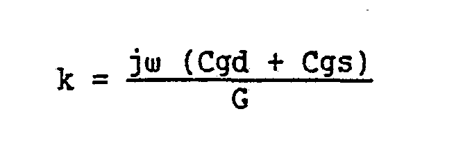
En ce qui concerne le déphasage, sa valeur est exacte pour f = 0 et se dégrade progressivement en hautes fréquences. On peut montrer que l'amélioration peut s'exprimer sous le forme équivalente du facteur K:
![]()
![]()
On obtient donc une amélioration en ce qui concerne la phase jusqu'à la fréquence de coupure du transistor.An improvement is therefore obtained with regard to the phase up to the cut-off frequency of the transistor.
Selon la figure 3, le déphaseur comporte un étage différentiel d'entrée comprenant deux transistors MESFET dont les sources sont couplées et connectées à une source de courant constituée par un transistor T28 dont la grille et la source sont connectées au pôle de tension d'alimentation négative U3, (par exemple -4V), et le drain connecté aux sources des transistors T2, et T23 précités. La tension d'entrée Ve est appliquée à la grille du transistor T2, à travers un réseau de découplage comportant un condensateur série C4 et une résistance parallèle R2 entre la grille du transistor T2, et le pôle de mode commun. La grille du transistor T23 est directement référencée au pôle de mode commun.According to FIG. 3, the phase shifter comprises a differential input stage comprising two MESFET transistors whose sources are coupled and connected to a current source constituted by a transistor T 28 whose gate and source are connected to the voltage pole of negative supply U 3 , (by example -4V), and the drain connected to the sources of the transistors T 2 , and T 23 above. The input voltage Ve is applied to the gate of transistor T 2 , through a decoupling network comprising a series capacitor C 4 and a parallel resistor R 2 between the gate of transistor T 2 , and the common mode pole. The gate of transistor T 23 is directly referenced to the common mode pole.
Afin d'obtenir un gain en dynamique tout en conservant un gain en continu de l'ordre de l'unité, les drains de transistors T2, et T23 sont associés à une charge active cons tituée par un transistor MESFET respectivement T22 et T24 dont la source est connectée au drain du transistor correspondant, et comportant un condensateur C3 de faible valeur ( de l'ordre du picofarad) connecté entre leur source et leur grille. La grille de chacun des transistors T22 et T24 est reliée à un pôle de tension d'alimentation U, (par exemple + 1,5V) à travers une résistance R,, alors que leur drain est connecté à un pôle de tension d'alimentation U2 (par exemple + 4V).In order to obtain a gain in dynamics while maintaining a gain in the order of unity, the transistor drains T 2 and T23 are associated with an active load constituted by a MESFET transistor T22 and T 24 respectively. the source of which is connected to the drain of the corresponding transistor, and comprising a capacitor C 3 of low value (of the order of picofarad) connected between their source and their gate. The gate of each of the transistors T22 and T 24 is connected to a supply voltage pole U, (for example + 1.5V) through a resistor R ,, while their drain is connected to a voltage pole of power supply U 2 (for example + 4V).
Des transistors T25 et T26 montés en suiveur et dont le drain est directement référencé à la source de tension U2 recoivent sur leur porte les tensions de drain respectivement des transistors T2, et Tu. Les sources des transistors T25 et T26 sont connectés chacun à un groupe de plusieurs diodes D en série, ici au nombre de 4, de manière à réaliser une adaptation de niveau pour les étages push-pull de sortie. Des transistors T27 et T29 montés en source de courant de manière analogue au transistor T28 ont leur drain connecté à la cathode de la dernière diode de chaque groupe, de manière à définir le courant traversant les diodes et donc la chute de tension dans celles-ci.Transistors T 25 and T 26 mounted as a follower and whose drain is directly referenced to the voltage source U 2 receive on their gate the drain voltages of the transistors T 2 and T u respectively . The sources of the transistors T 25 and T 26 are each connected to a group of several diodes D in series, here 4 in number, so as to perform a level adaptation for the push-pull output stages. Transistors T 27 and T29 mounted as a current source in a manner analogous to transistor T 28 have their drain connected to the cathode of the last diode of each group, so as to define the current passing through the diodes and therefore the voltage drop in those -this.
La source des transistors T25 et T26 est reliée à la porte respectivement des transistors T13 et T,, avec une chute de tension d'une diode, et à la porte respectivement des transistors T12 et T14 avec une chute de tension dans la totalité des diodes, à savoir quatre, ce qui permet de polariser correctement les étages de sortie. On pourra prendre dans cette configuration U, = 1,5V, U2 = 6V et U3 = -4V.The source of the transistors T 25 and T 26 is connected to the gate of the transistors T 13 and T, respectively, with a voltage drop of a diode, and to the gate of the transistors T 12 and T 14, respectively, with a voltage drop. in all of the diodes, namely four, which allows the output stages to be correctly polarized. We can take in this configuration U, = 1.5V, U 2 = 6V and U 3 = -4V.
Les figures 4a et 4b représentent un mode de réalisation préféré de l'invention dans lequel la valeur de l'écart de phase entre les sorties du déphaseur peut varier entre 0 et 180°.FIGS. 4a and 4b represent a preferred embodiment of the invention in which the value of the phase difference between the outputs of the phase shifter can vary between 0 and 180 °.
Selon la figure 4a, un module déphaseur (ϕ,, φ2) comporte deux branches en parallèle recevant le signal d'entrée. La première branche parallèle comporte un amplificateur A5 dont la sortie est chargée par deux résistances de même valeur en série Rs et R's, R's ayant une borne connectée au pôle de mode commun. La borne commune aux résistances R5 et R's constitue la sortie de la première branche. La deuxième branche parallèle comporte un amplificateur inverseur A6 dont la sortie est chargée par une résistance variable R6 dont la valeur est commandée par une tension V'e et un condensateur C6 dont une borne est connectée au pôle de mode commun. La borne commune à la résistance R6 et au condensateur C6 constitue la sortie de la deuxième branche.According to Figure 4a, a phase shift module (ϕ ,, φ 2 ) has two branches in parallel receiving the input signal. The first parallel branch comprises an amplifier A 5 whose output is charged by two resistors of the same value in series R s and R ' s , R' s having a terminal connected to the common mode pole. The terminal common to resistors R 5 and R ' s constitutes the output of the first branch. The second parallel branch comprises an inverting amplifier A 6 , the output of which is charged by a variable resistor R 6 , the value of which is controlled by a voltage V'e, and a capacitor C 6 , one terminal of which is connected to the common mode pole. The terminal common to the resistor R 6 and to the capacitor C 6 constitutes the output of the second branch.
Les sorties des deux branches sont additionnées par un sommateur 40 dont la sortie fournit un signal S.The outputs of the two branches are added by an
On a alors avec Rs = R's et les deux amplificateurs As et A6 ayant le même gain A :

Le déphasage pour une fréquence donnée dépend de la constante de temps r = R6C6. On a :![]()
![]()
On peut ainsi décrire un écart de phase Δφ variant de 0 à 180° suivant la valeur de r, donc de R6.We can thus describe a phase difference Δφ varying from 0 to 180 ° depending on the value of r, therefore of R 6 .
La figure 6b décrit un mode de réalisation particulièrement avantageux du déphaseur dans lequel l'écart de phase peut être réglé entre 0 et 180°, mettant en oeuvre un étage différentiel d'entrée MESFET à charge active, et un étage de sortie pour chaque amplificateur, mettant en oeuvre des transistors MESFET montés en push-pull, ce qui permet d'optimiser la tension résiduelle de mode commun.FIG. 6b describes a particularly advantageous embodiment of the phase shifter in which the phase difference can be adjusted between 0 and 180 °, implementing a differential input stage MESFET with active load, and an output stage for each amplifier , using MESFET transistors mounted in push-pull, which optimizes the common mode residual voltage.
On obtient donc une amélioration en ce qui concerne la phase jusqu'à la fréquence de coupure du transistor.An improvement is therefore obtained with regard to the phase up to the cut-off frequency of the transistor.
Les éléments similaires portent sur la figure 4b les mêmes références que sur la figure 3.Similar elements in FIG. 4b have the same references as in FIG. 3.
Les résistances Rs et R's sont raccordées en série entre la sortie de l'étage push-pull T,,, T12 et le pôle de mode commun avec interposition éventuelle d'un condensateur de découplage C5 de faible valeur. La résistance variable R6 est la résistance drain-source d'un transistor MESFET T36 dont le drain est connecté à la sortie de l'étage push-pull T13, T14 et dont la source est connectée à la borne non à la masse du condensateur CG. La grille du transistor T36 reçoit une tension V'e.Resistors R s and R ' s are connected in series between the output of the push-pull stage T ,,, T 12 and the common mode pole with possible interposition of a low-value decoupling capacitor C 5 . The variable resistance R 6 is the drain-source resistance of a MESFET transistor T 36 whose drain is connected to the output of the push-pull stage T 13 , T 14 and whose source is connected to the non-ground terminal of capacitor C G. The gate of transistor T 36 receives a voltage V ′ e .
Enfin, le sommateur 40 est constitué par deux transistors MESFET T31 et T32 dont les drains sont connectés à la source de tension d'alimentation U2, dont les sources sont couplées entre elles et connectées à transistor T33 monté en source de courant de manière analogue au transistor T28. La source du transistor T36 est connectée à la grille du transistor T32 et la borne commune aux résistances Rs et R's, à la grille du transistor T3,, ce qui fait que la somme de leurs tensions apparat sur les sources des transistors T31 et T32. (signal S). Pour faire varier l'écart de phase entre 0 et 180°, il faut faire varier la tension V'e jusqu'à atteindre la tension de pincement du canal du transistor T36.Finally, the
Claims (3)
Applications Claiming Priority (2)
| Application Number | Priority Date | Filing Date | Title |
|---|---|---|---|
| FR8700567 | 1987-01-20 | ||
| FR8700567A FR2609843B1 (en) | 1987-01-20 | 1987-01-20 | ACTIVE DEPHASEUR 0-180O FOR MICROWAVE |
Publications (2)
| Publication Number | Publication Date |
|---|---|
| EP0283056A1 true EP0283056A1 (en) | 1988-09-21 |
| EP0283056B1 EP0283056B1 (en) | 1991-11-06 |
Family
ID=9347052
Family Applications (1)
| Application Number | Title | Priority Date | Filing Date |
|---|---|---|---|
| EP88200006A Expired - Lifetime EP0283056B1 (en) | 1987-01-20 | 1988-01-06 | Active 0-180 degrees ultra high frequency phase shifter |
Country Status (5)
| Country | Link |
|---|---|
| US (1) | US4831336A (en) |
| EP (1) | EP0283056B1 (en) |
| JP (1) | JP2703245B2 (en) |
| DE (1) | DE3865989D1 (en) |
| FR (1) | FR2609843B1 (en) |
Families Citing this family (3)
| Publication number | Priority date | Publication date | Assignee | Title |
|---|---|---|---|---|
| US5061996A (en) * | 1989-06-29 | 1991-10-29 | Autovision Associates | Ground vehicle head up display for passenger |
| US5684429A (en) * | 1995-09-14 | 1997-11-04 | Ncr Corporation | CMOS gigabit serial link differential transmitter and receiver |
| US11183973B1 (en) | 2020-06-02 | 2021-11-23 | Samsung Electronics Co., Ltd | Method and circuit for power consumption reduction in active phase shifters |
Citations (1)
| Publication number | Priority date | Publication date | Assignee | Title |
|---|---|---|---|---|
| US3246241A (en) * | 1963-04-12 | 1966-04-12 | Lab For Electronics Inc | Variable phase shifter with internal readout |
Family Cites Families (1)
| Publication number | Priority date | Publication date | Assignee | Title |
|---|---|---|---|---|
| US4667165A (en) * | 1986-02-19 | 1987-05-19 | Advanced Micro Devices, Inc. | High-speed full differential amplifier with common mode rejection |
-
1987
- 1987-01-20 FR FR8700567A patent/FR2609843B1/en not_active Expired
-
1988
- 1988-01-06 EP EP88200006A patent/EP0283056B1/en not_active Expired - Lifetime
- 1988-01-06 DE DE8888200006T patent/DE3865989D1/en not_active Expired - Lifetime
- 1988-01-18 JP JP63007089A patent/JP2703245B2/en not_active Expired - Fee Related
- 1988-01-20 US US07/145,860 patent/US4831336A/en not_active Expired - Lifetime
Patent Citations (1)
| Publication number | Priority date | Publication date | Assignee | Title |
|---|---|---|---|---|
| US3246241A (en) * | 1963-04-12 | 1966-04-12 | Lab For Electronics Inc | Variable phase shifter with internal readout |
Non-Patent Citations (2)
| Title |
|---|
| GaAs IC SYMPOSIUM TECHNICAL DIGEST 1985, Monterey, Californie, 12-14 novembre 1985, pages 125-128, IEEE, US; Y.K. CHEN et al.: "A GaAs multi-band digitally-controlled 0 degrees - 360 degree phase shifter" * |
| JOURNAL OF THE AUDIO ENGINEERING SOCIETY, vol. 32, no. 6, juin 1984, pages 415-421, New York, US; S. TAKAHASHI et al.: "Fully balanced bridge amplifier" * |
Also Published As
| Publication number | Publication date |
|---|---|
| EP0283056B1 (en) | 1991-11-06 |
| JP2703245B2 (en) | 1998-01-26 |
| DE3865989D1 (en) | 1991-12-12 |
| US4831336A (en) | 1989-05-16 |
| FR2609843B1 (en) | 1989-04-21 |
| JPS63193712A (en) | 1988-08-11 |
| FR2609843A1 (en) | 1988-07-22 |
Similar Documents
| Publication | Publication Date | Title |
|---|---|---|
| EP0658977B1 (en) | Variable gain amplifier | |
| FR2475818A1 (en) | TUNNEL AND UNDERLYING CURRENT VOLTAGE REFERENCE FOR STANDARD "CMOS" INTEGRATED CIRCUIT | |
| FR2602380A1 (en) | GYRATOR CIRCUIT SIMULATING AN INDUCTANCE | |
| EP0278534B1 (en) | Broadband phase shifter | |
| FR2532115A1 (en) | CIRCUIT COMPRISING A VARIABLE TRANSCONDUCTANCE ELEMENT | |
| FR2478347A1 (en) | GAIN CONTROL SYSTEMS | |
| FR2621190A1 (en) | PROGRAMMABLE GAIN INSTRUMENTATION AMPLIFIER | |
| FR2529411A1 (en) | INTEGRATED CIRCUIT CURRENT AMPLIFIER WITH IMPROVED LINEARITY AND PRECISION OF CIRCUIT MULTIPLICATION COEFFICIENT | |
| FR2585201A1 (en) | DIFFERENTIAL OPERATIONAL AMPLIFIER FOR INTEGRATED CIRCUITS IN MOS TECHNOLOGY | |
| FR2476940A1 (en) | INTEGRATED CIRCUIT HAVING MULTIPLE VOLTAGE-CURRENT CONVERTER. | |
| FR3059493B1 (en) | REGULATING AN RF AMPLIFIER | |
| EP1380913A1 (en) | Linear voltage regulator | |
| EP0810728A1 (en) | Analog audio filter for high frequencies | |
| FR2527864A1 (en) | COMPRESSION NOISE REDUCTION CIRCUIT AND SIGNAL EXPANSION | |
| EP0283056A1 (en) | Active 0-180 degrees ultra high frequency phase shifter | |
| EP0737003A1 (en) | CCD register readout amplifier | |
| FR2487605A1 (en) | GAIN CONTROL CIRCUIT | |
| FR2661290A1 (en) | POWER AMPLIFIER, IN PARTICULAR FOR SQUARE SIGNALS. | |
| EP0308293B1 (en) | Controlled output power device for a class-c amplifier | |
| WO2000005818A1 (en) | Cmos output amplifier independent of temperature, supply voltage and manufacturing quality of transistors | |
| EP1313309A1 (en) | Calibrating device for a video input stage | |
| EP0305301B1 (en) | Signal compressor circuit, in particular for telephone set | |
| FR2664452A1 (en) | DEVICE FOR CORRECTING GAMMA ON ANALOGUE VIDEO SIGNAL. | |
| EP0263750B1 (en) | Sample and hold circuit with a high sample frequency | |
| FR2473745A1 (en) | HIGH RESOLUTION FAST DIODES LOCKED COMPARATOR |
Legal Events
| Date | Code | Title | Description |
|---|---|---|---|
| PUAI | Public reference made under article 153(3) epc to a published international application that has entered the european phase |
Free format text: ORIGINAL CODE: 0009012 |
|
| AK | Designated contracting states |
Kind code of ref document: A1 Designated state(s): DE FR GB IT |
|
| 17P | Request for examination filed |
Effective date: 19890301 |
|
| RAP1 | Party data changed (applicant data changed or rights of an application transferred) |
Owner name: N.V. PHILIPS' GLOEILAMPENFABRIEKEN Owner name: LABORATOIRES D'ELECTRONIQUE PHILIPS |
|
| 17Q | First examination report despatched |
Effective date: 19901205 |
|
| GRAA | (expected) grant |
Free format text: ORIGINAL CODE: 0009210 |
|
| AK | Designated contracting states |
Kind code of ref document: B1 Designated state(s): DE FR GB IT |
|
| REF | Corresponds to: |
Ref document number: 3865989 Country of ref document: DE Date of ref document: 19911212 |
|
| ITF | It: translation for a ep patent filed |
Owner name: ING. C. GREGORJ S.P.A. |
|
| GBT | Gb: translation of ep patent filed (gb section 77(6)(a)/1977) | ||
| PLBE | No opposition filed within time limit |
Free format text: ORIGINAL CODE: 0009261 |
|
| STAA | Information on the status of an ep patent application or granted ep patent |
Free format text: STATUS: NO OPPOSITION FILED WITHIN TIME LIMIT |
|
| 26N | No opposition filed | ||
| ITPR | It: changes in ownership of a european patent |
Owner name: CAMBIO RAGIONE SOCIALE;PHILIPS ELECTRONICS N.V. |
|
| REG | Reference to a national code |
Ref country code: FR Ref legal event code: CJ Ref country code: FR Ref legal event code: CD |
|
| REG | Reference to a national code |
Ref country code: FR Ref legal event code: TP |
|
| REG | Reference to a national code |
Ref country code: GB Ref legal event code: IF02 |
|
| REG | Reference to a national code |
Ref country code: GB Ref legal event code: 746 Effective date: 20020923 |
|
| REG | Reference to a national code |
Ref country code: FR Ref legal event code: D6 |
|
| PGFP | Annual fee paid to national office [announced via postgrant information from national office to epo] |
Ref country code: FR Payment date: 20030127 Year of fee payment: 16 |
|
| PGFP | Annual fee paid to national office [announced via postgrant information from national office to epo] |
Ref country code: GB Payment date: 20030131 Year of fee payment: 16 |
|
| PGFP | Annual fee paid to national office [announced via postgrant information from national office to epo] |
Ref country code: DE Payment date: 20030317 Year of fee payment: 16 |
|
| PG25 | Lapsed in a contracting state [announced via postgrant information from national office to epo] |
Ref country code: GB Free format text: LAPSE BECAUSE OF NON-PAYMENT OF DUE FEES Effective date: 20040106 |
|
| PG25 | Lapsed in a contracting state [announced via postgrant information from national office to epo] |
Ref country code: DE Free format text: LAPSE BECAUSE OF NON-PAYMENT OF DUE FEES Effective date: 20040803 |
|
| GBPC | Gb: european patent ceased through non-payment of renewal fee |
Effective date: 20040106 |
|
| PG25 | Lapsed in a contracting state [announced via postgrant information from national office to epo] |
Ref country code: FR Free format text: LAPSE BECAUSE OF NON-PAYMENT OF DUE FEES Effective date: 20040930 |
|
| REG | Reference to a national code |
Ref country code: FR Ref legal event code: ST |
|
| PG25 | Lapsed in a contracting state [announced via postgrant information from national office to epo] |
Ref country code: IT Free format text: LAPSE BECAUSE OF NON-PAYMENT OF DUE FEES;WARNING: LAPSES OF ITALIAN PATENTS WITH EFFECTIVE DATE BEFORE 2007 MAY HAVE OCCURRED AT ANY TIME BEFORE 2007. THE CORRECT EFFECTIVE DATE MAY BE DIFFERENT FROM THE ONE RECORDED. Effective date: 20050106 |