EP0282396A1 - Complex hybrid circuit structure, and its production method - Google Patents
Complex hybrid circuit structure, and its production method Download PDFInfo
- Publication number
- EP0282396A1 EP0282396A1 EP88400474A EP88400474A EP0282396A1 EP 0282396 A1 EP0282396 A1 EP 0282396A1 EP 88400474 A EP88400474 A EP 88400474A EP 88400474 A EP88400474 A EP 88400474A EP 0282396 A1 EP0282396 A1 EP 0282396A1
- Authority
- EP
- European Patent Office
- Prior art keywords
- substrate
- chips
- interconnections
- structure according
- welded
- Prior art date
- Legal status (The legal status is an assumption and is not a legal conclusion. Google has not performed a legal analysis and makes no representation as to the accuracy of the status listed.)
- Withdrawn
Links
Images


Classifications
-
- H—ELECTRICITY
- H05—ELECTRIC TECHNIQUES NOT OTHERWISE PROVIDED FOR
- H05K—PRINTED CIRCUITS; CASINGS OR CONSTRUCTIONAL DETAILS OF ELECTRIC APPARATUS; MANUFACTURE OF ASSEMBLAGES OF ELECTRICAL COMPONENTS
- H05K1/00—Printed circuits
- H05K1/02—Details
- H05K1/14—Structural association of two or more printed circuits
- H05K1/144—Stacked arrangements of planar printed circuit boards
-
- H—ELECTRICITY
- H01—ELECTRIC ELEMENTS
- H01L—SEMICONDUCTOR DEVICES NOT COVERED BY CLASS H10
- H01L23/00—Details of semiconductor or other solid state devices
- H01L23/12—Mountings, e.g. non-detachable insulating substrates
- H01L23/14—Mountings, e.g. non-detachable insulating substrates characterised by the material or its electrical properties
- H01L23/147—Semiconductor insulating substrates
-
- H—ELECTRICITY
- H01—ELECTRIC ELEMENTS
- H01L—SEMICONDUCTOR DEVICES NOT COVERED BY CLASS H10
- H01L23/00—Details of semiconductor or other solid state devices
- H01L23/34—Arrangements for cooling, heating, ventilating or temperature compensation ; Temperature sensing arrangements
- H01L23/36—Selection of materials, or shaping, to facilitate cooling or heating, e.g. heatsinks
- H01L23/367—Cooling facilitated by shape of device
- H01L23/3672—Foil-like cooling fins or heat sinks
-
- H—ELECTRICITY
- H01—ELECTRIC ELEMENTS
- H01L—SEMICONDUCTOR DEVICES NOT COVERED BY CLASS H10
- H01L23/00—Details of semiconductor or other solid state devices
- H01L23/52—Arrangements for conducting electric current within the device in operation from one component to another, i.e. interconnections, e.g. wires, lead frames
- H01L23/538—Arrangements for conducting electric current within the device in operation from one component to another, i.e. interconnections, e.g. wires, lead frames the interconnection structure between a plurality of semiconductor chips being formed on, or in, insulating substrates
- H01L23/5385—Assembly of a plurality of insulating substrates
-
- H—ELECTRICITY
- H01—ELECTRIC ELEMENTS
- H01L—SEMICONDUCTOR DEVICES NOT COVERED BY CLASS H10
- H01L23/00—Details of semiconductor or other solid state devices
- H01L23/58—Structural electrical arrangements for semiconductor devices not otherwise provided for, e.g. in combination with batteries
- H01L23/64—Impedance arrangements
- H01L23/642—Capacitive arrangements
-
- H—ELECTRICITY
- H01—ELECTRIC ELEMENTS
- H01L—SEMICONDUCTOR DEVICES NOT COVERED BY CLASS H10
- H01L24/00—Arrangements for connecting or disconnecting semiconductor or solid-state bodies; Methods or apparatus related thereto
- H01L24/01—Means for bonding being attached to, or being formed on, the surface to be connected, e.g. chip-to-package, die-attach, "first-level" interconnects; Manufacturing methods related thereto
- H01L24/42—Wire connectors; Manufacturing methods related thereto
- H01L24/47—Structure, shape, material or disposition of the wire connectors after the connecting process
- H01L24/49—Structure, shape, material or disposition of the wire connectors after the connecting process of a plurality of wire connectors
-
- H—ELECTRICITY
- H01—ELECTRIC ELEMENTS
- H01L—SEMICONDUCTOR DEVICES NOT COVERED BY CLASS H10
- H01L2224/00—Indexing scheme for arrangements for connecting or disconnecting semiconductor or solid-state bodies and methods related thereto as covered by H01L24/00
- H01L2224/01—Means for bonding being attached to, or being formed on, the surface to be connected, e.g. chip-to-package, die-attach, "first-level" interconnects; Manufacturing methods related thereto
- H01L2224/02—Bonding areas; Manufacturing methods related thereto
- H01L2224/04—Structure, shape, material or disposition of the bonding areas prior to the connecting process
- H01L2224/05—Structure, shape, material or disposition of the bonding areas prior to the connecting process of an individual bonding area
- H01L2224/0554—External layer
- H01L2224/0555—Shape
- H01L2224/05552—Shape in top view
- H01L2224/05554—Shape in top view being square
-
- H—ELECTRICITY
- H01—ELECTRIC ELEMENTS
- H01L—SEMICONDUCTOR DEVICES NOT COVERED BY CLASS H10
- H01L2224/00—Indexing scheme for arrangements for connecting or disconnecting semiconductor or solid-state bodies and methods related thereto as covered by H01L24/00
- H01L2224/01—Means for bonding being attached to, or being formed on, the surface to be connected, e.g. chip-to-package, die-attach, "first-level" interconnects; Manufacturing methods related thereto
- H01L2224/42—Wire connectors; Manufacturing methods related thereto
- H01L2224/44—Structure, shape, material or disposition of the wire connectors prior to the connecting process
- H01L2224/45—Structure, shape, material or disposition of the wire connectors prior to the connecting process of an individual wire connector
- H01L2224/45001—Core members of the connector
- H01L2224/45099—Material
- H01L2224/451—Material with a principal constituent of the material being a metal or a metalloid, e.g. boron (B), silicon (Si), germanium (Ge), arsenic (As), antimony (Sb), tellurium (Te) and polonium (Po), and alloys thereof
- H01L2224/45117—Material with a principal constituent of the material being a metal or a metalloid, e.g. boron (B), silicon (Si), germanium (Ge), arsenic (As), antimony (Sb), tellurium (Te) and polonium (Po), and alloys thereof the principal constituent melting at a temperature of greater than or equal to 400°C and less than 950°C
- H01L2224/45124—Aluminium (Al) as principal constituent
-
- H—ELECTRICITY
- H01—ELECTRIC ELEMENTS
- H01L—SEMICONDUCTOR DEVICES NOT COVERED BY CLASS H10
- H01L2224/00—Indexing scheme for arrangements for connecting or disconnecting semiconductor or solid-state bodies and methods related thereto as covered by H01L24/00
- H01L2224/01—Means for bonding being attached to, or being formed on, the surface to be connected, e.g. chip-to-package, die-attach, "first-level" interconnects; Manufacturing methods related thereto
- H01L2224/42—Wire connectors; Manufacturing methods related thereto
- H01L2224/44—Structure, shape, material or disposition of the wire connectors prior to the connecting process
- H01L2224/45—Structure, shape, material or disposition of the wire connectors prior to the connecting process of an individual wire connector
- H01L2224/45001—Core members of the connector
- H01L2224/45099—Material
- H01L2224/451—Material with a principal constituent of the material being a metal or a metalloid, e.g. boron (B), silicon (Si), germanium (Ge), arsenic (As), antimony (Sb), tellurium (Te) and polonium (Po), and alloys thereof
- H01L2224/45138—Material with a principal constituent of the material being a metal or a metalloid, e.g. boron (B), silicon (Si), germanium (Ge), arsenic (As), antimony (Sb), tellurium (Te) and polonium (Po), and alloys thereof the principal constituent melting at a temperature of greater than or equal to 950°C and less than 1550°C
- H01L2224/45144—Gold (Au) as principal constituent
-
- H—ELECTRICITY
- H01—ELECTRIC ELEMENTS
- H01L—SEMICONDUCTOR DEVICES NOT COVERED BY CLASS H10
- H01L2224/00—Indexing scheme for arrangements for connecting or disconnecting semiconductor or solid-state bodies and methods related thereto as covered by H01L24/00
- H01L2224/01—Means for bonding being attached to, or being formed on, the surface to be connected, e.g. chip-to-package, die-attach, "first-level" interconnects; Manufacturing methods related thereto
- H01L2224/42—Wire connectors; Manufacturing methods related thereto
- H01L2224/47—Structure, shape, material or disposition of the wire connectors after the connecting process
- H01L2224/48—Structure, shape, material or disposition of the wire connectors after the connecting process of an individual wire connector
- H01L2224/4805—Shape
- H01L2224/4809—Loop shape
- H01L2224/48091—Arched
-
- H—ELECTRICITY
- H01—ELECTRIC ELEMENTS
- H01L—SEMICONDUCTOR DEVICES NOT COVERED BY CLASS H10
- H01L2224/00—Indexing scheme for arrangements for connecting or disconnecting semiconductor or solid-state bodies and methods related thereto as covered by H01L24/00
- H01L2224/01—Means for bonding being attached to, or being formed on, the surface to be connected, e.g. chip-to-package, die-attach, "first-level" interconnects; Manufacturing methods related thereto
- H01L2224/42—Wire connectors; Manufacturing methods related thereto
- H01L2224/47—Structure, shape, material or disposition of the wire connectors after the connecting process
- H01L2224/48—Structure, shape, material or disposition of the wire connectors after the connecting process of an individual wire connector
- H01L2224/481—Disposition
- H01L2224/48151—Connecting between a semiconductor or solid-state body and an item not being a semiconductor or solid-state body, e.g. chip-to-substrate, chip-to-passive
- H01L2224/48153—Connecting between a semiconductor or solid-state body and an item not being a semiconductor or solid-state body, e.g. chip-to-substrate, chip-to-passive the body and the item being arranged next to each other, e.g. on a common substrate
- H01L2224/48195—Connecting between a semiconductor or solid-state body and an item not being a semiconductor or solid-state body, e.g. chip-to-substrate, chip-to-passive the body and the item being arranged next to each other, e.g. on a common substrate the item being a discrete passive component
-
- H—ELECTRICITY
- H01—ELECTRIC ELEMENTS
- H01L—SEMICONDUCTOR DEVICES NOT COVERED BY CLASS H10
- H01L2224/00—Indexing scheme for arrangements for connecting or disconnecting semiconductor or solid-state bodies and methods related thereto as covered by H01L24/00
- H01L2224/01—Means for bonding being attached to, or being formed on, the surface to be connected, e.g. chip-to-package, die-attach, "first-level" interconnects; Manufacturing methods related thereto
- H01L2224/42—Wire connectors; Manufacturing methods related thereto
- H01L2224/47—Structure, shape, material or disposition of the wire connectors after the connecting process
- H01L2224/48—Structure, shape, material or disposition of the wire connectors after the connecting process of an individual wire connector
- H01L2224/481—Disposition
- H01L2224/48151—Connecting between a semiconductor or solid-state body and an item not being a semiconductor or solid-state body, e.g. chip-to-substrate, chip-to-passive
- H01L2224/48221—Connecting between a semiconductor or solid-state body and an item not being a semiconductor or solid-state body, e.g. chip-to-substrate, chip-to-passive the body and the item being stacked
- H01L2224/48225—Connecting between a semiconductor or solid-state body and an item not being a semiconductor or solid-state body, e.g. chip-to-substrate, chip-to-passive the body and the item being stacked the item being non-metallic, e.g. insulating substrate with or without metallisation
- H01L2224/48227—Connecting between a semiconductor or solid-state body and an item not being a semiconductor or solid-state body, e.g. chip-to-substrate, chip-to-passive the body and the item being stacked the item being non-metallic, e.g. insulating substrate with or without metallisation connecting the wire to a bond pad of the item
-
- H—ELECTRICITY
- H01—ELECTRIC ELEMENTS
- H01L—SEMICONDUCTOR DEVICES NOT COVERED BY CLASS H10
- H01L2224/00—Indexing scheme for arrangements for connecting or disconnecting semiconductor or solid-state bodies and methods related thereto as covered by H01L24/00
- H01L2224/01—Means for bonding being attached to, or being formed on, the surface to be connected, e.g. chip-to-package, die-attach, "first-level" interconnects; Manufacturing methods related thereto
- H01L2224/42—Wire connectors; Manufacturing methods related thereto
- H01L2224/47—Structure, shape, material or disposition of the wire connectors after the connecting process
- H01L2224/49—Structure, shape, material or disposition of the wire connectors after the connecting process of a plurality of wire connectors
- H01L2224/491—Disposition
- H01L2224/49105—Connecting at different heights
- H01L2224/49109—Connecting at different heights outside the semiconductor or solid-state body
-
- H—ELECTRICITY
- H01—ELECTRIC ELEMENTS
- H01L—SEMICONDUCTOR DEVICES NOT COVERED BY CLASS H10
- H01L24/00—Arrangements for connecting or disconnecting semiconductor or solid-state bodies; Methods or apparatus related thereto
- H01L24/01—Means for bonding being attached to, or being formed on, the surface to be connected, e.g. chip-to-package, die-attach, "first-level" interconnects; Manufacturing methods related thereto
- H01L24/42—Wire connectors; Manufacturing methods related thereto
- H01L24/44—Structure, shape, material or disposition of the wire connectors prior to the connecting process
- H01L24/45—Structure, shape, material or disposition of the wire connectors prior to the connecting process of an individual wire connector
-
- H—ELECTRICITY
- H01—ELECTRIC ELEMENTS
- H01L—SEMICONDUCTOR DEVICES NOT COVERED BY CLASS H10
- H01L24/00—Arrangements for connecting or disconnecting semiconductor or solid-state bodies; Methods or apparatus related thereto
- H01L24/01—Means for bonding being attached to, or being formed on, the surface to be connected, e.g. chip-to-package, die-attach, "first-level" interconnects; Manufacturing methods related thereto
- H01L24/42—Wire connectors; Manufacturing methods related thereto
- H01L24/47—Structure, shape, material or disposition of the wire connectors after the connecting process
- H01L24/48—Structure, shape, material or disposition of the wire connectors after the connecting process of an individual wire connector
-
- H—ELECTRICITY
- H01—ELECTRIC ELEMENTS
- H01L—SEMICONDUCTOR DEVICES NOT COVERED BY CLASS H10
- H01L2924/00—Indexing scheme for arrangements or methods for connecting or disconnecting semiconductor or solid-state bodies as covered by H01L24/00
- H01L2924/0001—Technical content checked by a classifier
- H01L2924/00014—Technical content checked by a classifier the subject-matter covered by the group, the symbol of which is combined with the symbol of this group, being disclosed without further technical details
-
- H—ELECTRICITY
- H01—ELECTRIC ELEMENTS
- H01L—SEMICONDUCTOR DEVICES NOT COVERED BY CLASS H10
- H01L2924/00—Indexing scheme for arrangements or methods for connecting or disconnecting semiconductor or solid-state bodies as covered by H01L24/00
- H01L2924/01—Chemical elements
- H01L2924/01006—Carbon [C]
-
- H—ELECTRICITY
- H01—ELECTRIC ELEMENTS
- H01L—SEMICONDUCTOR DEVICES NOT COVERED BY CLASS H10
- H01L2924/00—Indexing scheme for arrangements or methods for connecting or disconnecting semiconductor or solid-state bodies as covered by H01L24/00
- H01L2924/01—Chemical elements
- H01L2924/01013—Aluminum [Al]
-
- H—ELECTRICITY
- H01—ELECTRIC ELEMENTS
- H01L—SEMICONDUCTOR DEVICES NOT COVERED BY CLASS H10
- H01L2924/00—Indexing scheme for arrangements or methods for connecting or disconnecting semiconductor or solid-state bodies as covered by H01L24/00
- H01L2924/01—Chemical elements
- H01L2924/01014—Silicon [Si]
-
- H—ELECTRICITY
- H01—ELECTRIC ELEMENTS
- H01L—SEMICONDUCTOR DEVICES NOT COVERED BY CLASS H10
- H01L2924/00—Indexing scheme for arrangements or methods for connecting or disconnecting semiconductor or solid-state bodies as covered by H01L24/00
- H01L2924/01—Chemical elements
- H01L2924/01047—Silver [Ag]
-
- H—ELECTRICITY
- H01—ELECTRIC ELEMENTS
- H01L—SEMICONDUCTOR DEVICES NOT COVERED BY CLASS H10
- H01L2924/00—Indexing scheme for arrangements or methods for connecting or disconnecting semiconductor or solid-state bodies as covered by H01L24/00
- H01L2924/01—Chemical elements
- H01L2924/01057—Lanthanum [La]
-
- H—ELECTRICITY
- H01—ELECTRIC ELEMENTS
- H01L—SEMICONDUCTOR DEVICES NOT COVERED BY CLASS H10
- H01L2924/00—Indexing scheme for arrangements or methods for connecting or disconnecting semiconductor or solid-state bodies as covered by H01L24/00
- H01L2924/01—Chemical elements
- H01L2924/01079—Gold [Au]
-
- H—ELECTRICITY
- H01—ELECTRIC ELEMENTS
- H01L—SEMICONDUCTOR DEVICES NOT COVERED BY CLASS H10
- H01L2924/00—Indexing scheme for arrangements or methods for connecting or disconnecting semiconductor or solid-state bodies as covered by H01L24/00
- H01L2924/013—Alloys
- H01L2924/0132—Binary Alloys
- H01L2924/01322—Eutectic Alloys, i.e. obtained by a liquid transforming into two solid phases
-
- H—ELECTRICITY
- H01—ELECTRIC ELEMENTS
- H01L—SEMICONDUCTOR DEVICES NOT COVERED BY CLASS H10
- H01L2924/00—Indexing scheme for arrangements or methods for connecting or disconnecting semiconductor or solid-state bodies as covered by H01L24/00
- H01L2924/013—Alloys
- H01L2924/014—Solder alloys
-
- H—ELECTRICITY
- H01—ELECTRIC ELEMENTS
- H01L—SEMICONDUCTOR DEVICES NOT COVERED BY CLASS H10
- H01L2924/00—Indexing scheme for arrangements or methods for connecting or disconnecting semiconductor or solid-state bodies as covered by H01L24/00
- H01L2924/10—Details of semiconductor or other solid state devices to be connected
- H01L2924/11—Device type
- H01L2924/14—Integrated circuits
-
- H—ELECTRICITY
- H01—ELECTRIC ELEMENTS
- H01L—SEMICONDUCTOR DEVICES NOT COVERED BY CLASS H10
- H01L2924/00—Indexing scheme for arrangements or methods for connecting or disconnecting semiconductor or solid-state bodies as covered by H01L24/00
- H01L2924/15—Details of package parts other than the semiconductor or other solid state devices to be connected
- H01L2924/151—Die mounting substrate
- H01L2924/1515—Shape
- H01L2924/15153—Shape the die mounting substrate comprising a recess for hosting the device
-
- H—ELECTRICITY
- H01—ELECTRIC ELEMENTS
- H01L—SEMICONDUCTOR DEVICES NOT COVERED BY CLASS H10
- H01L2924/00—Indexing scheme for arrangements or methods for connecting or disconnecting semiconductor or solid-state bodies as covered by H01L24/00
- H01L2924/15—Details of package parts other than the semiconductor or other solid state devices to be connected
- H01L2924/151—Die mounting substrate
- H01L2924/1517—Multilayer substrate
-
- H—ELECTRICITY
- H01—ELECTRIC ELEMENTS
- H01L—SEMICONDUCTOR DEVICES NOT COVERED BY CLASS H10
- H01L2924/00—Indexing scheme for arrangements or methods for connecting or disconnecting semiconductor or solid-state bodies as covered by H01L24/00
- H01L2924/15—Details of package parts other than the semiconductor or other solid state devices to be connected
- H01L2924/181—Encapsulation
-
- H—ELECTRICITY
- H01—ELECTRIC ELEMENTS
- H01L—SEMICONDUCTOR DEVICES NOT COVERED BY CLASS H10
- H01L2924/00—Indexing scheme for arrangements or methods for connecting or disconnecting semiconductor or solid-state bodies as covered by H01L24/00
- H01L2924/19—Details of hybrid assemblies other than the semiconductor or other solid state devices to be connected
- H01L2924/1901—Structure
- H01L2924/1904—Component type
- H01L2924/19041—Component type being a capacitor
-
- H—ELECTRICITY
- H01—ELECTRIC ELEMENTS
- H01L—SEMICONDUCTOR DEVICES NOT COVERED BY CLASS H10
- H01L2924/00—Indexing scheme for arrangements or methods for connecting or disconnecting semiconductor or solid-state bodies as covered by H01L24/00
- H01L2924/19—Details of hybrid assemblies other than the semiconductor or other solid state devices to be connected
- H01L2924/191—Disposition
- H01L2924/19101—Disposition of discrete passive components
- H01L2924/19105—Disposition of discrete passive components in a side-by-side arrangement on a common die mounting substrate
-
- H—ELECTRICITY
- H01—ELECTRIC ELEMENTS
- H01L—SEMICONDUCTOR DEVICES NOT COVERED BY CLASS H10
- H01L2924/00—Indexing scheme for arrangements or methods for connecting or disconnecting semiconductor or solid-state bodies as covered by H01L24/00
- H01L2924/30—Technical effects
- H01L2924/301—Electrical effects
- H01L2924/3011—Impedance
Definitions
- the invention relates to the manufacture of complex electronic circuits with several hundred thousand elementary components.
- hybrid circuits that is to say structures comprising several integrated circuit chips soldered on the same substrate; the chips are interconnected via bonded wires welded between each chip and an interconnection network formed on the substrate or in the substrate.
- the substrate is a cooked ceramic substrate with thick multilayer interconnections, it becomes very expensive if the layers are multiplied, the manufacturing yield becoming difficult to control.
- the substrate has conductive layers insulated from each other by insulating layers (polyimide for example) on which the interconnections are screen printed, it is then both expensive and poor heat sink.
- the invention proposes a new, less expensive hybrid circuit structure, achievable with technologies mastered today, allowing good heat dissipation of the energy consumed by the chips, and making it possible to produce very complex circuits with a space requirement which is practically the same as that which would be obtained with a technology of integration on whole slice.
- Another object of the invention is to allow the repair of the circuit in the event that a test carried out after assembly of the interconnections of the chips would show the need to replace a defective chip.
- the present invention has a hybrid circuit structure comprising several integrated circuit chips carried on a support serving as a heat sink and as an interconnection means between the chips, characterized in that the support consists of a first substrate on which the chips are directly transferred, a second substrate transferred to the first and pierced with openings at the location of the chips, the second substrate comprising a network of conductive interconnections and contact pads connected to these interconnections, connecting wires being welded between these areas and the chips.
- the first substrate can serve as a heat sink and its quality is not affected by the density of the network of interconnections since most, if not all, of the network of interconnections can be transferred to the second substrate. .
- the first substrate may be made of thermal conductive ceramic (alumina) and for the first substrate to be made of silicon, the network of interconnections being produced in monolithic integrated form in this second substrate.
- the second substrate incorporates electronic or analog electronic functions, also integrated.
- the power supply function which often requires larger conductors, will be reserved for the first substrate. Connecting wires will then be welded between the interconnections of the first substrate and the chips, in particular to bring to the chips by these wires two supply potentials Vdd and Vss and a ground potential Vgnd. However, most of the signal inteconnections between chips remain on the second substrate.
- the first substrate which will include conductive pads serving as output terminals to the outside of the hybrid circuit; connecting wires will then be soldered between interconnection conductors connected to these areas conductors and the contact pads of the second substrate, to bring input signals from the conductive pads to the chips and to bring output signals from the chips to the conductive pads, all via the interconnection network of the second substrate.
- a conventional hybrid circuit has been represented with its support fulfilling, depending on the case, various roles and in particular a role of mechanical support of the components of the circuit, a role of thermal dissipation of the energy consumed by the components , and a role of electrical interconnection of the components between them.
- the support is ceramic, for example alumina or alumina nitride or other electrically insulating and thermally conductive substances, if one wishes to reinforce the possibilities of heat dissipation.
- the interconnections between components can be located either on the surface of the support or inside the support itself, or a combination of the two.
- One way of making surface interconnections is the screen printing of conductive substances or the etching of conductive layers deposited on the surface.
- the screen-printed or surface-engraved interconnections can moreover be arranged on several layers to increase the possibilities of interconnections; then insulating layers (polyimide for example) are inserted between the various layers.
- One way of making interconnections within the support is to use thick multilayer cured ceramics, that is to say stacks of ceramic sheets covered with conductive screen-printed layers fired together.
- 10 is designated a co-baked ceramic support with internal interconnection layers 12 and 14 and a surface interconnection layer 16.
- Integrated circuit chips 18 and 20 have been shown.
- a protective cover for the circuit components is designated by the reference 22.
- interconnection layers 12, 14 and 16 are interconnected by vias internal to the support, not visible in the figure.
- the surface interconnection layer 16 in principle comprises conductive pads 24, 26 onto which the chips 18 and 20 are welded (welding by soft solder with a gold-silicon eutectic for example). It also includes conductive pads 28 located at the periphery of the support, outside the cover, these pads serving for the connection of the hybrid circuit to the outside.
- the surface interconnection layer comprises solder pads 30 on which conductive wires 32 (gold or aluminum) are welded, moreover welded to corresponding solder pads 34 provided on the integrated circuit chips.
- Figure 2 shows in another form the same type of hybrid structure.
- the view is in perspective, hood removed, and a single chip has been shown, however, four chip locations are provided.
- the superficial interconnections have been represented in a completely simplified manner.
- the references are the same as in FIG. 1.
- locations 36, 38 have also been shown for other components of the hybrid circuit and more particularly for power decoupling capacities that the 'We come to weld on the surface on portions of the interconnection layer connected to the power supplies of the circuit. All this is given only as an example.
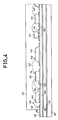
- Figure 3 a perspective view of the structure according to the invention, again by way of example only and in a very simplified form.
- the main characteristic of this structure is the use of a hybrid circuit support composed of the assembly of two substrates, the first substrate serving as mechanical support for the chips and heat sink, the second serving to produce most of it. interconnections between the chips.
- the second substrate is provided with openings surrounding the chips when the substrates are assembled one against the other (assembly by gluing, soldering, soldering etc.).
- the first substrate is designated by the reference 110, the second by the reference 140.
- Two openings 142, 144 have been shown in the second substrate and a chip 118, 120 is housed in each opening.
- the chips are transferred directly to the surface of the first substrate in the same manner as in the prior art, that is to say by bonding or soldering etc.
- An interconnection network 146 is formed in the second substrate, this network comprising not only interconnection conductors between the chips, but also conductive pads 148 which can be connected, in principle by soldered wires 149, to corresponding conductive pads 134 conventionally provided on integrated circuit chips.
- the conductive pads 148 are located near the edges of the openings 142,144 of the second substrate and if possible they are regularly distributed along these edges with a pitch which is the same as the pitch of the conductive pads 134 of the chips.
- the interconnection network 146 also comprises other conductive pads 150, which are located rather on the periphery of the second substrate, intended for connection with the outside of the second substrate. Although it is conceivable that these peripheral areas simply constitute the external access terminals of the hybrid circuit, it is preferable to provide that they are intermediate areas by which the interconnection network of the second substrate is connected to a surface interconnection layer of the first substrate.
- the first substrate is entirely analogous to the ceramic substrate of FIGS. 1 and 2: it is a thick multilayer ceramic substrate co-cooked with two internal interconnection layers 112 and 114 and a surface layer.
- the latter comprises on the one hand a certain number of interconnection conductors and on the other hand various conductive pads which can be: pads 124 and 126 on which the chips 118 and 120 are bonded or welded, pads 128 at the periphery of the first substrate, not covered by the second substrate and not covered by a protective cover 122 (shown in FIG. 4 only and which can be similar to that of FIG.
- pads 150 and pads 152 are soldered between pads 150 and pads 152 to provide connections between the interconnection network of the second substrate and the surface interconnection layer of the first substrate; - Optionally pads such as 156 located inside the openings of the second substrate so that a conductive wire can be soldered between a pad 156 and a corresponding pad of a chip; - possibly also other conductive pads such as 158 located either inside or outside the openings of the second substrate, these pads being intended to receive other components of the hybrid circuit (other hybrid circuit chips, capacitors power decoupling, other components transferred to the surface on the first substrate, etc.); by way of example, FIG.
- connection wires can be soldered between the chip and the upper part of an electrode of the capacitor, particularly in cases where it is desired to prevent wires do not extend between the chip and the first substrate at the bottom of the opening.
- the second substrate is preferably a monolithic integrated circuit substrate, so that the interconnection network which it carries can be produced by conventional monolithic integration technologies with the advantages that this entails in particular from the point of view of the interconnection density and cost of implementation. It should not be forgotten that a main object of the invention is to connect chips which can be very complex and have a large number of contact pads.
- the second substrate 140 is a silicon substrate; it can also be an insulating substrate.
- the interconnection network 146 is preferably produced by depositing and etching one or more layers of aluminum; if there are several layers, they are isolated from each other by deposited insulating layers (silicon oxide for example).
- the conductive pads of the second substrate are aligned along the edges of the openings 142 and 144 and distributed with the same pitch as the corresponding pads of the chips to which they are to be connected, so that a wiring of straight connecting wires between these areas (wires substantially all of the same length and of the same orientation).
- Such cabling has the advantage of being more reliable than conventional star cabling in the assembly of chips in a ceramic case.
- a network of pre-broadcast logic gates can be provided for example on the second substrate in order to be able to more easily customize the circuit according to the needs of the client.
- Figure 4 shows in a different form, in side section, the same type of structure as in Figure 3. the reference numerals are the same. A cover 122 has also been shown.
- the manufacturing of this structure will take place according to the following main stages: the first substrate is used, serving as mechanical support and heat sink, by conventional methods, by providing on this substrate, if desired, one or more layers of superimposed interconnection: in a preferred embodiment these layers will only comprise the supply conductors (a high potential conductor, a low potential conductor, and a conductor defining an electrical ground reference), the conductors interconnection proper between the chips being reserved for the second substrate because the impedance constraints of these interconnection conductors are less severe than those of the supply conductors.
- the supply conductors a high potential conductor, a low potential conductor, and a conductor defining an electrical ground reference
- the second substrate is prepared, for example in silicon: the interconnections are made according to conventional monolithic integration techniques, for example by the following sequence of steps (for a network with two layers of interconnections): - thick oxidation of the substrate, - aluminum deposition by evaporation, - etching of aluminum according to an interconnection pattern defined by a resin mask, - deposition of silicon oxide, - etching of the oxide to define contacts between the aluminum of the deposited layer and a subsequent layer, - deposit of a second layer of aluminum, - engraving of the second layer, - deposition of passivation silicon oxide, - etching of the oxide to define the contact pads 148 and 150 of FIG. 3.
- the production is more complex and corresponds to the production of conventional integrated circuit wafers.
- the openings (142, 144) of the second substrate are pierced by the following operations: - deposition of silicon nitride by plasma-assisted chemical decomposition (thickness about 1 micrometer), - nitride etching to define the locations of the openings (plasma etching in a high-speed reactor), - chemical etching with potash of the second substrate (silicon and oxide which covers it) where it is not protected by nitride, - Removal of the remaining nitride as well as of the silicon oxide possibly present on the rear face of the second substrate.
- the interconnection network of the second substrate is then tested via its conductive pads.
- the integrated circuits to be mounted on the hybrid circuit are manufactured according to a monolithic integration process appropriate to their complexity, they are tested, cut into individual chips, and the chips are transferred to the locations provided on the first substrate according to the usual techniques. in terms of mounting hybrid circuits or mounting chips in packages (soldering for example).
- the second substrate is transferred onto the first, for example by bonding using a conductive adhesive loaded with silver and polymerizable. In principle, most of the surface of the second substrate is bonded to a conductive pad of the first substrate.
- decoupling capacities or other components transferred flat on the first substrate are bonded.
- Wires are bonded between the conductive areas of the chips and the conductive areas of the second substrate and wires that may be necessary elsewhere, that is to say for example: - between conductive pads of the second substrate and conductive pads of the first, - between the chips and the first substrate, - between the chips and the electrodes of the decoupling capacities in certain cases.
- the protective cover is put in place and possibly, at the rear of the first substrate, a radiator is fixed.
- a hybrid circuit can be produced on a 6cm by 6cm support. comprising 9 very high integration integrated circuit chips, each having an area of approximately 1 cm 2 and having approximately 250 conductive pads for interfacing with the connection network of the second substrate.
- the size of this hybrid circuit then becomes of the same order as that of a monolithic integrated circuit on whole slice (WSI), at a lower cost.
- this technology makes it possible to mount chips produced in technologies which are different from each other on a common substrate.
Landscapes
- Engineering & Computer Science (AREA)
- Microelectronics & Electronic Packaging (AREA)
- Computer Hardware Design (AREA)
- Power Engineering (AREA)
- Physics & Mathematics (AREA)
- Condensed Matter Physics & Semiconductors (AREA)
- General Physics & Mathematics (AREA)
- Chemical & Material Sciences (AREA)
- Materials Engineering (AREA)
- Cooling Or The Like Of Semiconductors Or Solid State Devices (AREA)
Abstract
Description
L'invention concerne la fabrication des circuits électroniques complexes à plusieurs centaines de milliers de composants élémentaires.The invention relates to the manufacture of complex electronic circuits with several hundred thousand elementary components.
Pour réaliser ces circuits on utilise la technologie des circuits intégrés monolithiques de manière à limiter l'encombrement malgré le grand nombre de composants.To make these circuits, monolithic integrated circuit technology is used so as to limit the bulk despite the large number of components.
Mais cette technologie de miniaturisation extrême a des limites car les rendements de fabrication chutent considérablement lorsqu'on augmente la taille des puces de circuit intégré.However, this extreme miniaturization technology has limits because the manufacturing yields drop considerably when the size of the integrated circuit chips is increased.
Aujourd'hui on sait fabriquer avec un rendement faible mais acceptable, des puces de 1 cm de côté comportant environ 100 000 composants élémentaires. Certaines fonctions électroniques complexes peuvent nécessiter par exemple huit puces différentes de cette taille : par exemple des circuits de traitement de signal effectuant des transformées de fourier rapides.Today we know how to manufacture with a low but acceptable yield, chips of 1 cm side comprising about 100,000 elementary components. Some complex electronic functions may require, for example, eight different chips of this size: for example signal processing circuits performing fast fourier transforms.
Pour réaliser ces fonctions, on cherche actuellement des technologies d'intégration sur tranche entière (technologie WSI, de l'anglais "Wafer Scale Integration") : une tranche entière de semiconductor de plusieurs centimètres de diamètre comporterait non seulement l'ensemble des fonctions à réaliser mais aussi beaucoup de circuits de redondance destinés à pallier les défauts de fabrication qui ne manqueraient pas de se produire.To achieve these functions, we are currently looking for integration technologies on a whole slice (WSI technology, from the English "Wafer Scale Integration"): a whole slice of semiconductor several centimeters in diameter would not only include all of the functions to realize but also a lot of redundancy circuits intended to overcome the manufacturing defects which would not fail to occur.
Ces technologies WSI sont mal maitrisées aujourd'hui.These WSI technologies are poorly mastered today.
Une autre solution réside dans l'utilisation de circuits imprimés classiques sur lesquels on soude des boitiers enfermant chacune une puce de circuit intégré, le circuit imprimé servant à l'interconnexion des boitiers. Mais les puces comprises dans ces boitiers sont déjà des circuits intégrés complexes et les boitiers peuvent avoir chacun 200 à 250 broches de sortie et l'encombrement d'un boitier de 200 broches est de l'ordre de quatre centimètres de côté. L'ensemble du circuit imprimé avec plusieurs boitiers est donc très volumineux.Another solution lies in the use of conventional printed circuits on which boxes are welded each enclosing an integrated circuit chip, the printed circuit serving for the interconnection of the boxes. But the chips included in these boxes are already complex integrated circuits and the boxes can each have 200 to 250 output pins and the size of a 200-pin box is of the order of four centimeters aside. The entire printed circuit with several boxes is therefore very bulky.
Enfin, une autre solution consiste à utiliser des circuits hybrides, c'est à dire des structures comportant plusieurs puces de circuit intégré soudées sur un même substrat ; les puces sont reliées entre elles par l'intermédiaire de fils de liaison soudés entre chaque puce et un réseau d'interconnexion formé sur le substrat ou dans le substrat.Finally, another solution consists in using hybrid circuits, that is to say structures comprising several integrated circuit chips soldered on the same substrate; the chips are interconnected via bonded wires welded between each chip and an interconnection network formed on the substrate or in the substrate.
Le problème qu'on recontre avec les circuits hybrides est le suivant : il est difficile de réaliser sur ou dans le substrat des interconnexions très nombreuses qui seraient pourtant nécessaires compte-tenu de la complexité des puces à relier entre elles. Le pas des interconnexions est limité et si on veut faire passer de nombreuses interconnexions il faut que le substrat comporte de nombreuses couches d'interconnexion superposées.The problem encountered with hybrid circuits is as follows: it is difficult to make very numerous interconnections on or in the substrate which would nevertheless be necessary given the complexity of the chips to be connected together. The pitch of the interconnections is limited and if we want to pass many interconnections it is necessary that the substrate has many overlapping interconnection layers.
Si le substrat est un substrat de céramique cocuite à interconnexions multicouches épaisses, il devient très coûteux si on multiplie les couches, le rendement de fabrication devenant difficile à maîtriser.If the substrate is a cooked ceramic substrate with thick multilayer interconnections, it becomes very expensive if the layers are multiplied, the manufacturing yield becoming difficult to control.
Si le substrat comporte des couches conductrices isolées les unes des autres par des couches isolantes (polyimide par exemple) sur lesquelles on sérigraphie les interconnexions, il est alors à la fois coûteux et mauvais dissipateur thermique.If the substrate has conductive layers insulated from each other by insulating layers (polyimide for example) on which the interconnections are screen printed, it is then both expensive and poor heat sink.
L'invention propose une nouvelle structure de circuit hybride moins coûteuse, réalisable avec des technologies maîtrisées aujourd'hui, permettant une bonne dissipation thermique de l'énergie consommée par les puces, et permettant de réaliser des circuits très complexes avec un encombrement qui est pratiquement le même que celui qu'on obtiendrait avec une technologie d'intégration sur tranche entière.The invention proposes a new, less expensive hybrid circuit structure, achievable with technologies mastered today, allowing good heat dissipation of the energy consumed by the chips, and making it possible to produce very complex circuits with a space requirement which is practically the same as that which would be obtained with a technology of integration on whole slice.
Enfin, un autre but de l'invention est de permettre la réparation du circuit au cas où un test effectué après montage des interconnexions des puces montrerait la nécessité de remplacer une puce défectueuse.Finally, another object of the invention is to allow the repair of the circuit in the event that a test carried out after assembly of the interconnections of the chips would show the need to replace a defective chip.
Pour parvenir à ces résultats, la présente invention purpose une structure de circuit hybride comportant plusieurs puces de circuit-intégré reportées sur un support servant de dissipateur thermique et de moyen d'interconnexion entre les puces, caractérisé par le fait que le support est constitué par un premier substrat sur lequel sont directement reportées les puces, un deuxième substrat reporté sur le premier et percé d'ouvertures à l'emplacement des puces, le deuxième substrat comportant un réseau d'interconnexions conductrices et des plages de contact reliées à ces interconnexions, des fils de liaison étant soudés entre ces plages et les puces.To achieve these results, the present invention has a hybrid circuit structure comprising several integrated circuit chips carried on a support serving as a heat sink and as an interconnection means between the chips, characterized in that the support consists of a first substrate on which the chips are directly transferred, a second substrate transferred to the first and pierced with openings at the location of the chips, the second substrate comprising a network of conductive interconnections and contact pads connected to these interconnections, connecting wires being welded between these areas and the chips.
Ainsi, d'une part le premier substrat peut servir de dissipateur thermique et sa qualité n'est pas affectée par la densité du réseau d'interconnexions puisqu'on peut reporter la majeure partie sinon la totalité du réseau d'interconnexions sur le deuxième substrat.Thus, on the one hand, the first substrate can serve as a heat sink and its quality is not affected by the density of the network of interconnections since most, if not all, of the network of interconnections can be transferred to the second substrate. .
Dans ces conditions, on pourra prévoir que le premier substrat est en céramique conductrice thermique (alumine) et que le premier substrat est en silicium, le réseau d'interconnexions étant réalisé sous forme intégrée monolithique dans ce deuxième substrat. On peut même prévoir que le deuxième substrat incorpore des fonctions électroniques logiques ou analogiques, également intégrées.Under these conditions, provision may be made for the first substrate to be made of thermal conductive ceramic (alumina) and for the first substrate to be made of silicon, the network of interconnections being produced in monolithic integrated form in this second substrate. We can even foresee that the second substrate incorporates electronic or analog electronic functions, also integrated.
De préférence on réservera cependant au premier substrat la fonction d'alimentation en énergie qui souvent nécessite des conducteurs de plus grande dimension. Des fils de liaison seront alors soudés entre les interconnexions du premier substrat et les puces, en particulier pour amener aux puces par ces fils deux potentiels d'alimentation Vdd et Vss et un potentiel de masse Vgnd. Mais la majeure partie des inteconnexions de signal entre puces reste sur le deuxième substrat.Preferably, however, the power supply function, which often requires larger conductors, will be reserved for the first substrate. Connecting wires will then be welded between the interconnections of the first substrate and the chips, in particular to bring to the chips by these wires two supply potentials Vdd and Vss and a ground potential Vgnd. However, most of the signal inteconnections between chips remain on the second substrate.
En principe c'est le premier substrat qui comportera des plages conductrices servant de bornes de sortie vers l'extérieur du circuit hybride ; des fils de liaison seront alors soudés entre des conducteurs d'interconnexion reliés à ces plages conductrices et les plages de contact du deuxième substrat, pour amener des signaux d'entrée des plages conductrices vers les puces et pour amener des signaux de sortie des puces vers les plages conductrices, le tout par l'intermédiaire du réseau d'interconnexions du deuxième substrat.In principle, it is the first substrate which will include conductive pads serving as output terminals to the outside of the hybrid circuit; connecting wires will then be soldered between interconnection conductors connected to these areas conductors and the contact pads of the second substrate, to bring input signals from the conductive pads to the chips and to bring output signals from the chips to the conductive pads, all via the interconnection network of the second substrate.
Enfin, on verra comment la structure proposée rend assez aisée la mise en place de capacités de découplage d'alimentation qui sont souvent nécessaires dans les circuits hybrides complexes.Finally, we will see how the proposed structure makes it quite easy to set up supply decoupling capacities which are often necessary in complex hybrid circuits.
D'autres caractéristiques et avantages de l'invention apparaitront à la lecture de la description détaillée qui suit et qui est faite en référence aux dessins annexés dans lesquels :
- - la figure 1 représente en coupe schématique un circuit hybride classique
- - la figure 2 représente en perspective un circuit hybride classique
- - la figure 3 représente une vue en perspective de la structure selon l'invention
- - la figure 4 représente une vue en coupe d'une structure selon l'invention.
- - Figure 1 shows in schematic section a conventional hybrid circuit
- - Figure 2 shows in perspective a conventional hybrid circuit
- - Figure 3 shows a perspective view of the structure according to the invention
- - Figure 4 shows a sectional view of a structure according to the invention.
Sur la vue schématique de la figure 1, on a représenté un circuit hybride classique avec son support remplissant selon les cas divers rôles et notamment un rôle de support mécanique des composants du circuit, un rôle de dissipation thermique de l'énergie consommée par les composants, et un rôle d'interconnexion électrique des composants entre eux.In the diagrammatic view of FIG. 1, a conventional hybrid circuit has been represented with its support fulfilling, depending on the case, various roles and in particular a role of mechanical support of the components of the circuit, a role of thermal dissipation of the energy consumed by the components , and a role of electrical interconnection of the components between them.
Fréquemment le support est en céramique, par exemple en alumine ou en nitrure d'alumine ou d'autres substances électriquement isolantes et thermiquement conductrices, si on désire renforcer les possibilités de dissipation thermique.Frequently the support is ceramic, for example alumina or alumina nitride or other electrically insulating and thermally conductive substances, if one wishes to reinforce the possibilities of heat dissipation.
Les interconnexions entre composants peuvent être situées soit en surface du support soit à l'intérieur même du support, soit une combinaison des deux.The interconnections between components can be located either on the surface of the support or inside the support itself, or a combination of the two.
Une manière de réaliser des interconnexions en surface est la sérigraphie de substances conductrices ou la gravure de couches conductrices déposées en surface. Les interconnexions sérigraphiées ou gravées en surface peuvent d'ailleurs être disposées sur plusieurs couches pour accroître les possibilités d'interconnections; on intercale alors entre les diverses couches des couches isolantes (polyimide par exemple).One way of making surface interconnections is the screen printing of conductive substances or the etching of conductive layers deposited on the surface. The screen-printed or surface-engraved interconnections can moreover be arranged on several layers to increase the possibilities of interconnections; then insulating layers (polyimide for example) are inserted between the various layers.
Une manière de réaliser des interconnexions au sein du support est d'utiliser des céramiques cocuites multicouches épaisses, c'est-à-dire des empilements de feuilles de céramique recouvertes de couches conductrices sérigraphiées cuites ensemble.One way of making interconnections within the support is to use thick multilayer cured ceramics, that is to say stacks of ceramic sheets covered with conductive screen-printed layers fired together.
Ces supports de circuits hybrides ou même de puces decircuits intégrés isolées étant maintenant bien connus on ne rentrera pas dans le détail de leur réalisation.These supports for hybrid circuits or even isolated integrated circuit chips are now well known, so we will not go into detail about their implementation.
Sur la figure 1, on a désigné par 10 un support céramique cocuit avec des couches d'interconnexion interne 12 et 14 et une couche d'interconnexion superficielle 16. Des puces de circuit intégré 18 et 20 ont été représentées. Enfin un capot de protection des composants du circuit est désigné par la référence 22.In FIG. 1, 10 is designated a co-baked ceramic support with
Les couches d'interconnexions 12, 14 et 16 sont reliées entre elles par des vias internes au support, non visibles sur la figure.The
La couche d'interconnexion superficielle 16 comprend en principe des plages conductrices 24, 26 sur lesquelles sont soudées les puces 18 et 20 (soudage par brasure tendre avec un eutectique or-silicium par exemple). Elle comprend aussi des plages conductrices 28 situées à la périphérie du support, en dehors du capot, ces plages servant à la connexion du circuit hybride vers l'extérieur.The
Par ailleurs la couche d'interconnexion superficielle comprend des plages de soudure 30 sur lesquelles on vient souder des fils conducteurs 32 (or ou aluminium) soudés par ailleurs à des plages de soudure correspondantes 34 prévues sur les puces de circuit-intégré.Furthermore, the surface interconnection layer comprises
La figure 2 représente sous une autre forme le même type de structure hybride. La vue est en perspective, capot enlevé, et une seule puce a été représentée, quatre emplacements de puces étant cependant prévus. Les interconnexions superficielles ont été représentées de manière tout-à-fait simplifiée. Les références sont les mêmes qu'à la figure 1. Outre les quatre emplacements de puce, on a de plus représenté des emplacements 36, 38 pour d'autres composants du circuit hybride et tout particulièrement pour des capacités de découplage d'alimentation que l'on vient souder en surface sur des portions de couche d'interconnexion reliées aux alimentations en énergie du circuit. Tout ceci n'est donné qu'à titre d'exemple.Figure 2 shows in another form the same type of hybrid structure. The view is in perspective, hood removed, and a single chip has been shown, however, four chip locations are provided. The superficial interconnections have been represented in a completely simplified manner. The references are the same as in FIG. 1. In addition to the four chip locations,
Pour bien faire comprendre l'invention, on a représenté à la figure 3 une vue en perspective de la structure selon l'invention, là encore à titre d'exemple seulement et sous une forme très simplifiée.To clearly understand the invention, there is shown in Figure 3 a perspective view of the structure according to the invention, again by way of example only and in a very simplified form.
La caractéristique principale de cette structure est l'utilisation d'un support de circuit hybride composé de l'assemblage de deux substrats, le premier substrat servant de support mécanique pour les puces et de dissipateur de chaleur, le deuxième servant à réaliser la majeure partie des interconnexions entre les puces. Le deuxième substrat est pourvu d'ouvertures entourant les puces lorsque les substrats sont assemblés l'un contre l'autre (assemblage par collage, brasure, soudure etc.).The main characteristic of this structure is the use of a hybrid circuit support composed of the assembly of two substrates, the first substrate serving as mechanical support for the chips and heat sink, the second serving to produce most of it. interconnections between the chips. The second substrate is provided with openings surrounding the chips when the substrates are assembled one against the other (assembly by gluing, soldering, soldering etc.).
Le premier substrat est désigné par la référence 110, le deuxième par la référence 140. Deux ouvertures 142,144 ont été représentées dans le deuxième substrat et une puce 118,120 est logée dans chaque ouverture. Les puces sont reportées directement sur la surface du premier substrat de la même manière que dans la technique antérieure, c'est-à-dire par collage ou brasure etc.The first substrate is designated by the
Un réseau d'interconnexions 146 est formé dans le deuxième substrat, ce réseau comportant non seulement des conducteurs d'interconnexion entre les puces, mais aussi des plages conductrices 148 que l'on pourra relier, en principe par des fils soudés 149, à des plages conductrices correspondantes 134 prévues classiquement sur les puces de circuit-intégré.An
On prévoit de préférence que les plages conductrices 148 sont situées à proximité des bords des ouvertures 142,144 du deuxième substrat et si possible on les répartit régulièrement le long de ces bords avec un pas qui est le même que le pas des plages conductrices 134 des puces.It is preferably provided that the
Le réseau d'interconnexions 146 comprend par ailleurs d'autre plages conductrices 150, situées quant à elles plutôt à la périphérie du deuxième substrat, destinées à la liaison avec l'extérieur du deuxième substrat. Bien que l'on puisse envisager que ces plages périphériques constituent tout simplement les bornes d'accès extérieur du circuit hybride, il est préférable de prévoir qu'elles sont des plages intermédiaires par lesquelles le réseau d'interconnexion du deuxième substrat est relié à une couche d'interconnexion superficielle du premier substrat.The
C'est ce qui est prévu dans l'exemple de réalisation de la figure 3 où le premier substrat est tout-à-fait analogue au substrat de céramique des figures 1 et 2: c'est un substrat de céramique multicouche épaisse cocuite avec deux couches d'interconnexion internes 112 et 114 et une couche superficielle. Cette dernière comporte d'une part un certain nombre de conducteurs d'interconnexion et d'autre part diverses plages conductrices qui peuvent être:
- des plages 124 et 126 sur lesquelles on vient coller ou souder les puces 118 et 120,
- des plages 128 à la périphérie du premier substrat, non recouvertes par le deuxième substrat et non recouvertes par un capot de protection 122 (représenté à la figure 4 seulement et pouvant être analogue à celui de la figure 1), ces plages servant de bornes d'accès extérieur pour le circuit hybride,
- des plages 152 de préférence proches de plages 150 de la périphérie du deuxième substrat; des fils conducteurs 154 sont soudés entre les plages 150 et les plages 152 pour assurer les liaisons entre le réseau d'interconnexion du deuxième substrat et la couche d'interconnexion superficielle du premier substrat;
- éventuellement des plages telles que 156 localisées à l'intérieur des ouvertures du deuxième substrat de sorte qu'un fil conducteur peut être soudé entre une plage 156 et une plage correspondante d'une puce;
- éventuellement encore d'autres plages conductrices telles que 158 situées soit à l'intérieur soit à l'extérieur des ouvertures du deuxième substrat, ces plages étant destinées à recevoir d'autres composants du circuit hybride (autres puces de circuit hybride, capacités de découplage d'alimentation, autres composants reportés en surface sur le premier substrat, etc.); à titre d'exemple on a représenté sur la figure 3 une capacité de découplage d'alimentation 160 dont les électrodes sont soudées sur des plages conductrices du premier substrat à l'intérieur de l'ouverture 144 du deuxième substrat; cette capacité est située de préférence dans un angle de l'ouverture (supposée carrée ou rectangulaire) de sorte qu'elle ne gêne pas le passage des fils soudés entre les puces et le deuxième substrat (les fils s'étendant de préférence perpendiculairement aux bords de l'ouverture); enfin, en variante de montage de la capacité de découplage 160, on prévoit que des fils de connexion peuvent être soudés entre la puce et la partie supérieure d'une électrode de la capacité, particulièrement dans les cas où l'on veut éviter que des fils ne s'étendent entre la puce et le premier substrat au fond de l'ouverture.This is what is provided for in the exemplary embodiment of FIG. 3 where the first substrate is entirely analogous to the ceramic substrate of FIGS. 1 and 2: it is a thick multilayer ceramic substrate co-cooked with two internal interconnection layers 112 and 114 and a surface layer. The latter comprises on the one hand a certain number of interconnection conductors and on the other hand various conductive pads which can be:
-
- Optionally pads such as 156 located inside the openings of the second substrate so that a conductive wire can be soldered between a
- possibly also other conductive pads such as 158 located either inside or outside the openings of the second substrate, these pads being intended to receive other components of the hybrid circuit (other hybrid circuit chips, capacitors power decoupling, other components transferred to the surface on the first substrate, etc.); by way of example, FIG. 3 shows a
Le deuxième substrat est de préférence un substrat de circuit-intégré monolithique, de sorte que le réseau d'interconnexion qu'il porte peut être réalisé par les technologies d'intégration monolithiques classiques avec les avantages que cela entraîne notamment du point de vue de la densité d'interconnexion et du coût de réalisation. Il ne faut pas perdre de vue qu'un but principal de l'invention est de connecter entre elles des puces qui peuvent être très complexes et à grand nombre de plages de contact.The second substrate is preferably a monolithic integrated circuit substrate, so that the interconnection network which it carries can be produced by conventional monolithic integration technologies with the advantages that this entails in particular from the point of view of the interconnection density and cost of implementation. It should not be forgotten that a main object of the invention is to connect chips which can be very complex and have a large number of contact pads.
Dans un mode de réalisation le deuxième substrat 140 est un substrat de silicium; ce peut être aussi un substrat isolant. Le réseau d'interconnexion 146 est de préférence réalisé par dépôt et gravure d'une ou plusieurs couches d'aluminium; s'il y a plusieurs couches, elles sont isolées les unes des autres par des couches isolantes déposées (oxyde de silicium par exemple).In one embodiment, the
Il est particulièrement intéressant de prévoir que les plages conductrices du deuxième substrat sont alignées le long des bords des ouvertures 142 et 144 et réparties avec le même pas que les plages correspondantes des puces auxquelles elles doivent être reliées, de sorte qu'on peut réaliser un câblage de fils de liaison droit entre ces plages (fils sensiblement tous de même longueur et de même orientation). Un tel câblage a l'avantage d'être plus fiable qu'un câblage en étoile classique dans le montage de puces en boîtier céramique.It is particularly advantageous to provide that the conductive pads of the second substrate are aligned along the edges of the
Dans certains cas on pourra prévoir d'intégrer dans ce deuxième substrat monolithique non seulement un réseau de conducteurs d'interconnexion mais aussi des éléments de circuit réalisant des fonctions électroniques logiques ou analogiques. Un réseau de portes logiques prédiffusées peut être prévu par exemple sur le deuxième substrat afin de pouvoir plus facilement personnaliser le circuit en fonction des besoins du client.In certain cases, provision may be made to integrate into this second monolithic substrate not only a network of interconnection conductors but also circuit elements performing electronic logic or analog functions. A network of pre-broadcast logic gates can be provided for example on the second substrate in order to be able to more easily customize the circuit according to the needs of the client.
La figure 4 représente sous une forme différente, en coupe latérale, le même type de structure qu'à la figure 3. les références numériques sont les mêmes. Un capot 122 a été représenté en outre.Figure 4 shows in a different form, in side section, the same type of structure as in Figure 3. the reference numerals are the same. A
La fabrication de cette structure se déroulera selon les principales étapes suivantes: on fabrique le premier substrat servant de support mécanique et de dissipateur de chaleur, par des méthodes classiques, en prévoyant sur ce substrat, si on le désire, une ou plusieurs couches d'interconnexion superposées: dans une réalisation préférentielle ces couches comporteront seulement les conducteurs d'alimentation (un conducteur à potentiel haut, un conducteur à potentiel bas, et un conducteur définissant une référence de masse électrique), les conducteurs d'interconnexion proprement dits entre les puces étant réservés au deuxième substrat car les contraintes d'impédance de ces conducteurs d'interconnexion sont moins sévères que celles des conducteurs d'alimentation.The manufacturing of this structure will take place according to the following main stages: the first substrate is used, serving as mechanical support and heat sink, by conventional methods, by providing on this substrate, if desired, one or more layers of superimposed interconnection: in a preferred embodiment these layers will only comprise the supply conductors (a high potential conductor, a low potential conductor, and a conductor defining an electrical ground reference), the conductors interconnection proper between the chips being reserved for the second substrate because the impedance constraints of these interconnection conductors are less severe than those of the supply conductors.
Par ailleurs on prépare le deuxième substrat, par exemple en silicium: les interconnexions sont réalisées selon des techniques d'intégration monolithiques classiques, par exemple par la succession d'étapes suivantes (pour un réseau à deux couches d'interconnexions) :
- oxydation épaisse du substrat,
- dépôt d'aluminium par évaporation,
- gravure de l'aluminium selon un motif d'interconnexions défini par un masque de résine,
- dépôt d'oxyde de silicium,
- gravure de l'oxyde pour définir des contacts entre l'aluminium de la couche déposée et une couche ultérieure,
- dépôt d'une deuxième couche d'aluminium,
- gravure de la deuxième couche,
- dépôt d'oxyde de silicium de passivation,
- gravure de l'oxyde pour définir les plages de contact 148 et 150 de la figure 3.Furthermore, the second substrate is prepared, for example in silicon: the interconnections are made according to conventional monolithic integration techniques, for example by the following sequence of steps (for a network with two layers of interconnections):
- thick oxidation of the substrate,
- aluminum deposition by evaporation,
- etching of aluminum according to an interconnection pattern defined by a resin mask,
- deposition of silicon oxide,
- etching of the oxide to define contacts between the aluminum of the deposited layer and a subsequent layer,
- deposit of a second layer of aluminum,
- engraving of the second layer,
- deposition of passivation silicon oxide,
- etching of the oxide to define the
Bien entendu, si le deuxième substrat comporte des circuits actifs en plus de réseau d'interconnexion, la réalisation est plus complexe et correspond à la réalisation de tranches de circuit intégré classiques.Of course, if the second substrate comprises active circuits in addition to an interconnection network, the production is more complex and corresponds to the production of conventional integrated circuit wafers.
On procède ensuite au perçage des ouvertures (142, 144) du deuxième substrat, par les opérations suivantes:
- dépôt de nitrure de silicium par décomposition chimique assistée par plasma (épaisseur environ 1 micromètre),
- gravure du nitrure pour définir les emplacements des ouvertures (gravure au plasma dans un réacteur à grande vitesse),
- gravure chimique à la potasse du deuxième substrat (silicium et oxyde qui le recouvre) là où il n'est pas protégé par du nitrure,
- enlèvement du nitrure qui subsiste ainsi que de l'oxyde de silicium éventuellement présent sur la face arrière du deuxième substrat.Next, the openings (142, 144) of the second substrate are pierced by the following operations:
- deposition of silicon nitride by plasma-assisted chemical decomposition (thickness about 1 micrometer),
- nitride etching to define the locations of the openings (plasma etching in a high-speed reactor),
- chemical etching with potash of the second substrate (silicon and oxide which covers it) where it is not protected by nitride,
- Removal of the remaining nitride as well as of the silicon oxide possibly present on the rear face of the second substrate.
Le réseau d'interconnexion du deuxième substrat est alors testé par l'intermédiaire de ses plages conductrices.The interconnection network of the second substrate is then tested via its conductive pads.
Les circuits-intégrés à monter sur le circuit hybride sont fabriqués selon un procédé d'intégration monolithique approprié à leur complexité, ils sont testés, découpés en puces individuelles, et les puces sont reportées sur les emplacements prévus sur le premier substrat selon les techniques habituelles en matière de montage de circuits hybrides ou de montage de puces en boîtier (brasage par exemple).The integrated circuits to be mounted on the hybrid circuit are manufactured according to a monolithic integration process appropriate to their complexity, they are tested, cut into individual chips, and the chips are transferred to the locations provided on the first substrate according to the usual techniques. in terms of mounting hybrid circuits or mounting chips in packages (soldering for example).
On reporte le deuxième substrat sur le premier, par exemple par collage à l'aide d'une colle conductrice chargée à l'argent et polymérisable. En principe la majeure partie de la surface du deuxième substrat est collée sur une plage conductrice du premier substrat.The second substrate is transferred onto the first, for example by bonding using a conductive adhesive loaded with silver and polymerizable. In principle, most of the surface of the second substrate is bonded to a conductive pad of the first substrate.
On colle éventuellement des capacités de découplage ou d'autres composants reportés à plat sur le premier substrat.Optionally, decoupling capacities or other components transferred flat on the first substrate are bonded.
On soude des fils de liaison entre les plages conductrices des puces et les plages conductrices du deuxième substrat et des fils éventuellement nécessaires ailleurs, c'est-à-dire par exemple:
- entre des plages conductrices du deuxième substrat et des plages conductrices du premier,
- entre les puces et le premier substrat,
- entre les puces et les électrodes des capacités de découplage dans certains cas.Wires are bonded between the conductive areas of the chips and the conductive areas of the second substrate and wires that may be necessary elsewhere, that is to say for example:
- between conductive pads of the second substrate and conductive pads of the first,
- between the chips and the first substrate,
- between the chips and the electrodes of the decoupling capacities in certain cases.
On teste le circuit hybride, s'il y a lieu on désoude une puce qui s'avérerait défectueuse et on la remplace par une autre.We test the hybrid circuit, if necessary we remove a chip that turns out to be defective and replace it with another.
Enfin on met en place le capot de protection et éventuellement, à l'arrière du premier substrat, on fixe un radiateur.Finally, the protective cover is put in place and possibly, at the rear of the first substrate, a radiator is fixed.
A titre d'exemple des possibilités de l'invention, on peut réaliser sur un support de 6cm par 6cm un circuit hybride comportant 9 puces de circuit-intégré à très haute intégration, chacune ayant une surface d'environ 1cm² et ayant environ 250 plages conductrices d'interface avec le réseau de connexion du deuxième substrat. L'encombrement de ce circuit hybride devient alors du même ordre que celui d'un circuit monolithique intégré sur tranche entière (WSI), à un coùt plus faible. De plus, cette technologie permet de monter des puces réalisées dans des technologies différentes les unes des autres sur un substrat commun.As an example of the possibilities of the invention, a hybrid circuit can be produced on a 6cm by 6cm support. comprising 9 very high integration integrated circuit chips, each having an area of approximately 1 cm 2 and having approximately 250 conductive pads for interfacing with the connection network of the second substrate. The size of this hybrid circuit then becomes of the same order as that of a monolithic integrated circuit on whole slice (WSI), at a lower cost. In addition, this technology makes it possible to mount chips produced in technologies which are different from each other on a common substrate.
Claims (10)
- préparer un premier substrat (110) servant de dissipateur thermique
- préparer un deuxième substrat (140) comportant un réseau d'interconnexions et des plages de contact (148, 150), le deuxième substrat (140) étant percé d'ouvertures (142, 144) pouvant servir de logement aux puces,
- reporter les puces et le deuxième substrat sur le premier substrat, les puces étant situées dans les ouvertures du deuxième substrat,
- souder des fils de liaison (149) entre les puces et des plages de contact (148) du deuxième substrat.10. A method of manufacturing a hybrid circuit structure, comprising the steps of transferring integrated circuit chips (118, 120) onto a support serving as a heat sink for the chips, and interconnecting the chips via of the support, a process characterized by the operations consisting of
- prepare a first substrate (110) serving as a heat sink
preparing a second substrate (140) comprising an interconnection network and contact pads (148, 150), the second substrate (140) being pierced with openings (142, 144) which can serve as housing for the chips,
- transfer the chips and the second substrate to the first substrate, the chips being located in the openings of the second substrate,
- solder connecting wires (149) between the chips and contact pads (148) of the second substrate.
Applications Claiming Priority (2)
| Application Number | Priority Date | Filing Date | Title |
|---|---|---|---|
| FR8702832A FR2611986B1 (en) | 1987-03-03 | 1987-03-03 | COMPLEX HYBRID CIRCUIT STRUCTURE AND MANUFACTURING METHOD |
| FR8702832 | 1987-03-03 |
Publications (1)
| Publication Number | Publication Date |
|---|---|
| EP0282396A1 true EP0282396A1 (en) | 1988-09-14 |
Family
ID=9348525
Family Applications (1)
| Application Number | Title | Priority Date | Filing Date |
|---|---|---|---|
| EP88400474A Withdrawn EP0282396A1 (en) | 1987-03-03 | 1988-03-01 | Complex hybrid circuit structure, and its production method |
Country Status (2)
| Country | Link |
|---|---|
| EP (1) | EP0282396A1 (en) |
| FR (1) | FR2611986B1 (en) |
Cited By (5)
| Publication number | Priority date | Publication date | Assignee | Title |
|---|---|---|---|---|
| FR2647961A1 (en) * | 1989-05-30 | 1990-12-07 | Thomson Composants Militaires | Multichip electronic circuit, in ceramic housing with interconnection chip |
| WO1992006496A1 (en) * | 1990-10-06 | 1992-04-16 | Robert Bosch Gmbh | Multi-film hybrid circuit with power components |
| WO1998007193A1 (en) * | 1996-08-09 | 1998-02-19 | Robert Bosch Gmbh | Multichip module |
| EP0831530A2 (en) * | 1996-09-19 | 1998-03-25 | Murata Manufacturing Co., Ltd. | Integrated dielectric substrate |
| EP0841694A1 (en) * | 1995-12-08 | 1998-05-13 | Shinko Electric Industries Co. Ltd. | Semiconductor package with multilayered circuit and semiconductor device |
Citations (2)
| Publication number | Priority date | Publication date | Assignee | Title |
|---|---|---|---|---|
| FR2181892A2 (en) * | 1967-02-02 | 1973-12-07 | Bunker Ramo | |
| DE3511722A1 (en) * | 1984-04-02 | 1985-10-03 | Burroughs Corp. (n.d. Ges. des Staates Delaware), Detroit, Mich. | ELECTROMECHANICAL ASSEMBLY FOR INTEGRATED CIRCUIT MATRICES |
-
1987
- 1987-03-03 FR FR8702832A patent/FR2611986B1/en not_active Expired
-
1988
- 1988-03-01 EP EP88400474A patent/EP0282396A1/en not_active Withdrawn
Patent Citations (2)
| Publication number | Priority date | Publication date | Assignee | Title |
|---|---|---|---|---|
| FR2181892A2 (en) * | 1967-02-02 | 1973-12-07 | Bunker Ramo | |
| DE3511722A1 (en) * | 1984-04-02 | 1985-10-03 | Burroughs Corp. (n.d. Ges. des Staates Delaware), Detroit, Mich. | ELECTROMECHANICAL ASSEMBLY FOR INTEGRATED CIRCUIT MATRICES |
Non-Patent Citations (2)
| Title |
|---|
| IBM TECHNICAL DISCLOSURE BULLETIN, vol. 21, no. 5, octobre 1978, pages 1895-1897, New York, US; S. MAGDO: "Low inductance module" * |
| IEEE TRANSACTIONS ON COMPONENTS, HYBRIDS, AND MANUFACTURING TECHNOLOGY, vol. CHMT-7, no. 2, juin 1984, pages 193-196, IEEE, New York, US; R.K. SPIELBERGER et al.: "Silicon-on-silicon packaging" * |
Cited By (9)
| Publication number | Priority date | Publication date | Assignee | Title |
|---|---|---|---|---|
| FR2647961A1 (en) * | 1989-05-30 | 1990-12-07 | Thomson Composants Militaires | Multichip electronic circuit, in ceramic housing with interconnection chip |
| WO1992006496A1 (en) * | 1990-10-06 | 1992-04-16 | Robert Bosch Gmbh | Multi-film hybrid circuit with power components |
| EP0841694A1 (en) * | 1995-12-08 | 1998-05-13 | Shinko Electric Industries Co. Ltd. | Semiconductor package with multilayered circuit and semiconductor device |
| EP0841694A4 (en) * | 1995-12-08 | 1998-11-25 | Shinko Electric Ind Co | Semiconductor package with multilayered circuit and semiconductor device |
| US5994771A (en) * | 1995-12-08 | 1999-11-30 | Shinko Electric Industries Co., Inc. | Semiconductor package with multilayer circuit, and semiconductor device |
| WO1998007193A1 (en) * | 1996-08-09 | 1998-02-19 | Robert Bosch Gmbh | Multichip module |
| US5953213A (en) * | 1996-08-09 | 1999-09-14 | Robert Bosch Gmbh | Multichip module |
| EP0831530A2 (en) * | 1996-09-19 | 1998-03-25 | Murata Manufacturing Co., Ltd. | Integrated dielectric substrate |
| EP0831530A3 (en) * | 1996-09-19 | 2000-03-22 | Murata Manufacturing Co., Ltd. | Integrated dielectric substrate |
Also Published As
| Publication number | Publication date |
|---|---|
| FR2611986A1 (en) | 1988-09-09 |
| FR2611986B1 (en) | 1989-12-08 |
Similar Documents
| Publication | Publication Date | Title |
|---|---|---|
| EP0133125B1 (en) | Electronic component housing with a capacitor | |
| EP0583201B1 (en) | Three-dimensional multichip module | |
| EP0228953B1 (en) | Encapsulation housing for an electronic circuit | |
| US9368476B2 (en) | Stacked microelectronic assembly with TSVs formed in stages with plural active chips | |
| EP0310463A1 (en) | Housing for a high-density integrated circuit | |
| EP0325068B1 (en) | Modular hybrid microelectronic structure with high integration density | |
| WO2008054660A2 (en) | Wafer-level fabrication of lidded chips with electrodeposited dielectric coating | |
| FR2735648A1 (en) | COOLING METHOD OF AN INTEGRATED CIRCUIT MOUNTED IN A HOUSING | |
| FR2645681A1 (en) | Vertical interconnection device for integrated-circuit chips and its method of manufacture | |
| FR2990297A1 (en) | STACK OF SEMICONDUCTOR STRUCTURES AND METHOD OF MANUFACTURING THE SAME | |
| EP0282396A1 (en) | Complex hybrid circuit structure, and its production method | |
| EP0166634B1 (en) | Electric voltage dividing device and electronic component containing a package including such a device | |
| FR3077925A1 (en) | THREE DIMENSIONAL INTEGRATED CIRCUIT FACING A SIMPLIFIED STRUCTURE | |
| WO2018002368A1 (en) | Electronic device comprising an integrated bank of passive components | |
| EP0431106B1 (en) | Packaged electronic circuit with a chip on a gridded area of conductive pads | |
| FR2579022A1 (en) | ELECTRONIC CIRCUIT ASSEMBLY COMPRISING AT LEAST ONE INTEGRATED CIRCUIT ELEMENT | |
| FR3123147A1 (en) | Ball array type flip chip integrated circuit package for very high frequency operation. | |
| EP1210690A1 (en) | Electronic device comprising a chip fixed on a support and method for making same | |
| FR2647961A1 (en) | Multichip electronic circuit, in ceramic housing with interconnection chip | |
| FR2496341A1 (en) | Compact topological interconnection device - localises nodes and crossovers of complex circuit formed on single layer support with connections formed by metal strips | |
| FR2618255A1 (en) | PACKAGING BLOCK FOR MOUNTING AND INTERCONNECTING SEMICONDUCTOR CHIPS. | |
| FR2611412A1 (en) | Laminated interconnection card | |
| KR20120060727A (en) | Stacked microelectronic assembly with tsvs formed in stages with plural active chips | |
| FR2904472A1 (en) | METHOD FOR MANUFACTURING ENCAPSULE INTEGRATED CIRCUIT AND INTEGRATED ENCAPSULE INTEGRATED CIRCUIT |
Legal Events
| Date | Code | Title | Description |
|---|---|---|---|
| PUAI | Public reference made under article 153(3) epc to a published international application that has entered the european phase |
Free format text: ORIGINAL CODE: 0009012 |
|
| AK | Designated contracting states |
Kind code of ref document: A1 Designated state(s): CH DE GB IT LI SE |
|
| 17P | Request for examination filed |
Effective date: 19880930 |
|
| 17Q | First examination report despatched |
Effective date: 19910123 |
|
| STAA | Information on the status of an ep patent application or granted ep patent |
Free format text: STATUS: THE APPLICATION IS DEEMED TO BE WITHDRAWN |
|
| 18D | Application deemed to be withdrawn |
Effective date: 19911017 |