EP0280799B1 - Antennensystem für breitbandige Signale - Google Patents
Antennensystem für breitbandige Signale Download PDFInfo
- Publication number
- EP0280799B1 EP0280799B1 EP87301829A EP87301829A EP0280799B1 EP 0280799 B1 EP0280799 B1 EP 0280799B1 EP 87301829 A EP87301829 A EP 87301829A EP 87301829 A EP87301829 A EP 87301829A EP 0280799 B1 EP0280799 B1 EP 0280799B1
- Authority
- EP
- European Patent Office
- Prior art keywords
- pulses
- pulse
- charging
- coupled
- antenna
- Prior art date
- Legal status (The legal status is an assumption and is not a legal conclusion. Google has not performed a legal analysis and makes no representation as to the accuracy of the status listed.)
- Expired - Lifetime
Links
- 230000005404 monopole Effects 0.000 claims description 23
- 238000007599 discharging Methods 0.000 claims description 14
- 230000008878 coupling Effects 0.000 claims description 5
- 238000010168 coupling process Methods 0.000 claims description 5
- 238000005859 coupling reaction Methods 0.000 claims description 5
- 238000011084 recovery Methods 0.000 claims description 2
- 230000001902 propagating effect Effects 0.000 claims 3
- 230000001934 delay Effects 0.000 claims 1
- 238000000034 method Methods 0.000 description 6
- 238000010586 diagram Methods 0.000 description 5
- 230000001960 triggered effect Effects 0.000 description 4
- 230000005540 biological transmission Effects 0.000 description 3
- 238000002955 isolation Methods 0.000 description 3
- 230000005855 radiation Effects 0.000 description 3
- 230000005284 excitation Effects 0.000 description 2
- 239000012811 non-conductive material Substances 0.000 description 2
- 239000006096 absorbing agent Substances 0.000 description 1
- 239000011358 absorbing material Substances 0.000 description 1
- 239000003990 capacitor Substances 0.000 description 1
- 239000004020 conductor Substances 0.000 description 1
- 230000003287 optical effect Effects 0.000 description 1
- 230000000630 rising effect Effects 0.000 description 1
- 230000035945 sensitivity Effects 0.000 description 1
Images


Classifications
-
- H—ELECTRICITY
- H01—ELECTRIC ELEMENTS
- H01Q—ANTENNAS, i.e. RADIO AERIALS
- H01Q21/00—Antenna arrays or systems
- H01Q21/06—Arrays of individually energised antenna units similarly polarised and spaced apart
- H01Q21/08—Arrays of individually energised antenna units similarly polarised and spaced apart the units being spaced along or adjacent to a rectilinear path
- H01Q21/12—Parallel arrangements of substantially straight elongated conductive units
-
- G—PHYSICS
- G01—MEASURING; TESTING
- G01S—RADIO DIRECTION-FINDING; RADIO NAVIGATION; DETERMINING DISTANCE OR VELOCITY BY USE OF RADIO WAVES; LOCATING OR PRESENCE-DETECTING BY USE OF THE REFLECTION OR RERADIATION OF RADIO WAVES; ANALOGOUS ARRANGEMENTS USING OTHER WAVES
- G01S13/00—Systems using the reflection or reradiation of radio waves, e.g. radar systems; Analogous systems using reflection or reradiation of waves whose nature or wavelength is irrelevant or unspecified
- G01S13/02—Systems using reflection of radio waves, e.g. primary radar systems; Analogous systems
- G01S13/0209—Systems with very large relative bandwidth, i.e. larger than 10 %, e.g. baseband, pulse, carrier-free, ultrawideband
-
- G—PHYSICS
- G01—MEASURING; TESTING
- G01S—RADIO DIRECTION-FINDING; RADIO NAVIGATION; DETERMINING DISTANCE OR VELOCITY BY USE OF RADIO WAVES; LOCATING OR PRESENCE-DETECTING BY USE OF THE REFLECTION OR RERADIATION OF RADIO WAVES; ANALOGOUS ARRANGEMENTS USING OTHER WAVES
- G01S7/00—Details of systems according to groups G01S13/00, G01S15/00, G01S17/00
- G01S7/02—Details of systems according to groups G01S13/00, G01S15/00, G01S17/00 of systems according to group G01S13/00
- G01S7/03—Details of HF subsystems specially adapted therefor, e.g. common to transmitter and receiver
-
- H—ELECTRICITY
- H01—ELECTRIC ELEMENTS
- H01Q—ANTENNAS, i.e. RADIO AERIALS
- H01Q21/00—Antenna arrays or systems
- H01Q21/0006—Particular feeding systems
- H01Q21/0025—Modular arrays
-
- H—ELECTRICITY
- H01—ELECTRIC ELEMENTS
- H01Q—ANTENNAS, i.e. RADIO AERIALS
- H01Q9/00—Electrically-short antennas having dimensions not more than twice the operating wavelength and consisting of conductive active radiating elements
- H01Q9/005—Electrically-short antennas having dimensions not more than twice the operating wavelength and consisting of conductive active radiating elements for radiating non-sinusoidal waves
-
- H—ELECTRICITY
- H03—ELECTRONIC CIRCUITRY
- H03K—PULSE TECHNIQUE
- H03K3/00—Circuits for generating electric pulses; Monostable, bistable or multistable circuits
- H03K3/02—Generators characterised by the type of circuit or by the means used for producing pulses
- H03K3/335—Generators characterised by the type of circuit or by the means used for producing pulses by the use, as active elements, of semiconductor devices with more than two electrodes and exhibiting avalanche effect
Definitions
- This invention pertains to the field of airborne antennas and more specifically to antennas mounted on a cylindrical metallic surface with limited extensions therefrom for radiating and receiving signals with very wide instantaneous bandwidths.
- Constraints on antenna system design are determined by the instantaneous bandwidth of the radiated signal, the desired spatial distribution of that signal, the desired relation and reception efficiency, and dimensional limitations for a particular application.
- design parameters to meet these objectives are generally well known.
- the fractional bandwidth becomes very wide (50% to 100%)
- This wide signal bandwidth condition suggests quasi-optical or time delay techniques as effective antenna design procedures.
- the quasi-optical approach wherein reflectors, lenses, and horns, though dispersive, are utilised to achieve the design objectives has found greater acceptance.
- space constraints and the dispersive characteristics of the optical techniques establish the time delay technique as a more suitable approach.
- the present invention is defined in the appended claims and utilises time delay techniques to provide wide instantaneous bandwidth signal antennas mounted on a cylindrical metallic surface, such as the fuselage of a missile or small aircraft, that do not significantly extend above the surface.
- a wide instantaneous bandwidth signal radiation and reception system embodying the principles of the present invention may include a linear array of capped monopoles positioned on the surface of a cylinder in a parallel relationship with the cylinders axis.
- Each element in the array is energised by one of a plurality of pulse generators which are sequentially triggered with intervening time intervals corresponding to the antenna element spacing, thus establishing a radiation pattern with a peak in the direction of the sequential order.
- Radar reflections are received by an antenna comprised of a capped monopole coupled via a switch to a receiver internal to the cylinder and a second capped monopole positioned as a reflecting element.
- Isolation between the receiving monopole and the transmitting monopole array is achieved by diametrically positioning the receiving and transmitting elements on the cylindrical surface, splitting the cylindrical surface in a plane perpendicular to an axis in line with the receiving and transmitting elements, placing a non-conducting material between the two cylindrical sections so formed to substantially reduce surface currents, and decoupling the receiver from the receiving antenna during transmissions by maintaining the switch therebetween in the open position during this interval.
- Antennas that may be employed with the system of the present invention are shown mounted on a cylindrical surface in Figure 1.
- An array 11 of antenna elements 11a till11n, each of which may be a capped monopole that protrudes radially from the surface of a cylinder 12 along a line 13 that is substantially parallel to the cylinder axis 14, may be employed as a transmitting antenna by sequentially exciting the elements 11a through 11n, as will be discussed hereinafter.
- the caps 15a through 15n on each monopole 16a through 16n are of a diameter that is substantially equal to the height of the monopole, which may be for example less that ct r , where t r is the rise time of the pulse to be radiated from the antenna element and c is the speed of light.
- the spacing s between the elements 11a till 11a may be substantially equal to the distance travelled by a signal during the sequential interval between the excitation of adjacent elements. This arrangement forms a beam in the direction indicated by arrow 17 when the elements are excited in sequence from 11n to 11a.
- a receiving antenna positioned on the cylinder 12 diametrically from the transmitting antenna 11 may comprise an active element 22 and a reflecting element 23, shorted to the cylindrical surface 12, each of which may be a conical monopole.
- the active and reflecting elements 22, 23 are shaped to minimise impedance mismatches to the feeding transmission line.
- Capped conical monopoles with half cone angles of 47°, shown in Figure 1, at heights of approximately ⁇ o /8 and spacing d of substantially ⁇ o /4 ( ⁇ o being the wavelength at the centre frequency in the band) provide a minimum mismatch to a 50 ohm transmission line when the cap diameter of the active element 22 is substantially equal to the element height, and the cap diameter of the reflecting element 23 is substantially equal to twice the element height.
- the half cone angle of 47° is not critical and deviations therefrom may be practiced without significantly altering the match to the feed line.
- capped monopole and capped conical monopoles are not limitative and that other antenna types, such as capped discones, may be employed. Additionally, it should be recognised that like elements may be employed for the transmitting array and receiving antenna.
- Capped monopoles and capped conical monopoles possess impedance characteristics that may be readily matched, respectively, to the impedances of the transmitter and receiver, each yet to be described, utilised in the preferred embodiment of the present invention.
- each element in the transmitting antenna 11 When each element in the transmitting antenna 11 is energised, currents are induced on the cylindrical surface 12 which is coupled to the receiving antenna 21. These currents may be of sufficient amplitude to damage the receiver coupled to the active element 22 and limit the minimum operational range of the radar system. These currents may be significantly reduced by longitudinally cutting the cylindrical surface into two equal parts and replacing the sections thereby removed with electrical absorbing or non-conductive material 24. Significant decoupling between the transmitting and receiving antennas may be accomplished in this manner. Additional decoupling in many applications may be required. This may be accomplished by coupling a switch between the active element of the receiving antenna and the receiver as will be described subsequently.
- a pulse generator suitable for driving the capped monopole elements of the transmitting array 11 is shown in Figure 2.
- This pulse is coupled via an isolation delay line 27 and charging inductance 28 to charge a multiplicity of charge storage devices in which may be serially-coupled diodes 31 of the step recovery type (stack of diodes).
- the pulse coupled through the delay line 27 is also coupled via a capacitor 32 to over-voltage the collector 33a of a transistor 33, which may be of the type known in the art as MPSU04, causing it to avalanche at a time prdetermined by the bias voltages applied thereto.
- the voltage across the stack 31 "snaps" from a level of substantially zero to a level of the order of -200 volts over an interval of approximately 200ps and returns to a level of substantially 0 volts in a comparable time, thereby establishing a pulse of substantially 400ps duration at node 34, wherefrom it is coupled to a capped monopole 35.
- An increase in radiated power may be obtained by providing a linear array of elements sequentially fed, such that the pulses from each radiating element coalesce at the final excited element during its excitation interval to provide a radiated beam in a desired direction.
- an avalanche transistor 36 triggered by a pulse coupled to its base from an input terminal 37 substantially simultaneously charges diode stacks 41 to 44 via isolation delay lines 41a to 44a and charging inductors 41b to 44b, as previously described.
- Pulses from the delay lines 41a through 44a are also coupled to over-voltage the collectors of transistors 41c to 44c which thereafter avalanche in a sequence determined by the bias voltages established by the setting of potentiometers 41d to 44d and a positive voltage source not shown. Pulses sequentially generated by the diode stacks 41 to 44 are coupled via lines 41e to 44e to the array elements 41f to 44f, respectively.
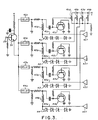
- Avalanche transistors are temperature sensitive, thereby subjecting antenna characteristics that depend upon the sequential operation of a multiplicity of avalanche transistors to performance variations that are functions of temperature. This temperature sensitivity may be minimised by discharging the diode stack through a common avalanche transistor.
- a charging avalanche transistor 51 and discharging avalanche transistor 52 are triggered with a time interval therebetween by a trigger generator 53 to couple charging and discharging pulses via delay lines 54 and 55, respectively, to a node 56.
- the charging and discharging signals, with the time interval therebetween, are coupled via delay lines 57a, 58a, 59a and 60a to diode stacks 57, 58, 59 and 60, respectively, in sequence, the sequential interval being determined by delay lines 57a-60a.
- Each of the diode stacks 57-60 charges and discharges in the manner previously described to sequentially excite the antenna elements 57b, 58b, 59b and 60b having a spacing therebetween corresponding to the sequential interval.
- This circuit charges all the diode stacks through a single transistor, and discharges all the diode stacks through another transistor, thus eliminating transistor temperature variations that may cause variations in the sequential interval and the width of the radiated pulses. It should be recognised that the single discharge transistor may be replaced with a stack of transistor when an amplitude is desired that cannot be achieved with the utilisation of a single transistor.
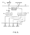
- FIG. 5 shows a block diagram of the equipment coupled to the transmitting array 11 and receiving antenna 21 of Figure 1.
- the main limitation upon the minimum detectable range of the short pulse radar system is the direct coupled signal from the transmitter 73 to the receiver 74.
- a large amplitude signal, directly coupled from the transmitter to the receiver, may trigger the detector therein, even if its is biased off or the range gate is closed.
- an absorber may be positioned between the two sections of the cylinder to reduce direct coupling due to surface currents. Further reduction of direct coupling may be obtained with a switch 75 positioned in the circuit between the receiving anenna 72 and the receiver 74.
- the switch 75 may be a SPST PIN diode controlled by a switch control generator 76.
- Trigger pulses may be coupled to the switch control generator 76 from a transmitter 73 and may be the same pulses used to trigger the charging pulse generator 51.
Landscapes
- Engineering & Computer Science (AREA)
- Radar, Positioning & Navigation (AREA)
- Remote Sensing (AREA)
- Computer Networks & Wireless Communication (AREA)
- Physics & Mathematics (AREA)
- General Physics & Mathematics (AREA)
- Variable-Direction Aerials And Aerial Arrays (AREA)
- Radar Systems Or Details Thereof (AREA)
Claims (16)
- Kurzpuls-Antennensystem,
gekennzeichnet durch Vorrichtungen (26) zur Erzeugung von Triggerimpulsen; Ladungsvorrichtungen (25), die auf den Triggerimpuls hin Ladungsimpulse erzeugen; Impulsvorrichtungen (31) die sich auf einen Impuls von der Ladungsvorrichtung hin aufladen; Vorrichtungen (31, 41 bis 44) die auf die Ladungsvorrichtung hin ansprechen und mit der Pulsvorrichtung verbunden sind, um Entladungsimpulse an vorbestimmten Zeitintervallen nach den Ladungsimpulsen an die Impulsvorrichtungen zu schicken um die Impulsvorrichtungen zu entladen und eine Sequenz von kurzen Impulsen vorbestimmter Dauer und vorbestimmter Anstiegszeit zu erzeugen wobei dazwischen ein vorbestimmtes Zeitintervall liegt; und einer Anordnung von Antennenelementen (11a...11n), die auf Impulse von der Impulsvorrichtung in einer entsprechenden Sequenz zur Erzeugung von ausgesendeten Impulsen ansprechen, wobei die Antennenelemente einen Abstand (S) voneinander haben, der der Distanz entspricht, die Licht im freien Raum in einer Zeit zurücklegt, die dem vorbestimmten Zeitintervall entspricht. - System nach Anspruch 1,
dadurch gekennzeichnet, daß die Anordnung der Antennenelemente aus mit Kappen versehenen Monopolantennen (11a...11n) besteht, wobei die Höhe der Monopolantennen geringer ist, als die Distanz, die Licht in freiem Raum in jener vorbestimmten Anstiegszeit zurücklegt und der Durchmesser der Kappe auf ihr der Höhe der Monopolantenne entspricht. - System nach Anspruch 1 oder 2,
dadurch gekennzeichnet, daß die Impulsvorrichtungen (31) eine Mehrzahl von Ladungsspeicherelementen aufweisen, die von jenen Ladungs- und Entladungsvorrichtungen ge- und entladen werden, um die kurzen Impulse zu erzeugen. - System nach Anspruch 3,
dadurch gekennzeichnet, daß die Ladungsspeicherelemente eine Vielzahl von in Reihe geschalteten Speicherschaltdioden aufweisen. - Kurzpuls-Antennensystem,
gekennzeichnet durch Vorrichtungen (53) zur Erzeugung eines Triggerimpulses;
Ladungsvorrichtungen (51) die auf den Triggerimpuls ansprechen und einen Ladungsimpuls erzeugen;
Entladungsvorrichtungen (52) die auf den Triggerimpuls ansprechen und an einen vorbestimmten Zeitpunkt nach dem Ladungsimpuls einen Entladungsimpuls erzeugen; und
Impulsvorrichtung (57-60) die mit der Ladungsvorrichtung und der Entladungsvorrichtung verbunden ist und zur Erzeugung einer Sequenz von kurzen Impulsen mit der vorbestimmten Anstiegszeit auf die Ladungs- und Entladungsimpulse anspricht, wobei die Sequenz vorbestimmte Zeitintervalle zwischen den Pulsen hat; und
eine Vielzahl von Antennenelementen (57b-60b) die auf die kurzen Impulse in einer korrespondierenden Sequenz zur Erzeugung von abgestrahlten Impulsen ansprechen, wobei die Antennenelemente einen Abstand (S) zwischeneinander haben, der der Entfernung entspricht, die Licht im freien Raum in einer Zeit zurücklegt, die der des vorbestimmten Zeitintervalls entspricht. - System nach Anspruch 5,
gekennzeichnet durch eine Impulsvorrichtung (57-60), mit einer Vielzahl von Ladungsspeicherelementen, die alle von der Ladungs- bzw. Entladungsvorrichtung ge- bzw. entladen werden, um einen kurzen Impuls mit einer vorbestimmten Anstiegszeit zu erzeugen und mit einer Vielzahl von Verzögerungselementen (57a-60a) zur Erzeugung von jeweils unterschiedlichen Zeitverzögerungen, die mit den Ladungsvorrichtungen und den Entladungsvorrichtungen und in entsprechender Weise mit der Vielzahl der Ladungsspeicherelemente verbunden sind, so daS die Ladungs- und Entladungsimpulse zu den Ladungsspeicherelementen mit Zeitintervallen dazwischen gelangen können, um jene Sequenz von kurzen Impulsen zu erzeugen. - System nach Anspruch 5 oder 6,
dadurch gekennzeichnet, daß die Ladungsvorrichtungen (51) und Entladungsvorrichtungen (52) Avalanchetransistoren enthalten. - System nach Anspruch 6 oder 7,
dadurch gekennzeichnet, daß jedes Ladungsspeicherelement (57 bis 60) eine Vielzahl von in Reihe geschalteten Speicherschaltdioden enthält. - System nach einen der vorstehenden Ansprüche,
dadurch gekennzeichnet, daß die Antennenelemente Monopolantennen mit Kappen (11a...11n) sind. - System nach einem der vorstehenden Ansprüche,
gekennzeichnet durch weitere Antennenvorrichtungen (22, 23) zum Empfangen von Reflektionen der abgestrahlten Impulse. - System nach Anspruch 10,
dadurch gekennzeichnet, daß die empfangende Antennenvorrichtung ein Beschickungsantennenelement (22) und ein Reflektionsantennenelement (23) enthält. - System nach Anpruch 11,
dadurch gekennzeichnet, daß das Beschickungsantennenelement (22) und das Reflektionsantennenelement (23) Diskon-Antennen sind. - System nach Anspruch 11,
dadurch gekennzeichnet, daß die Beschickungs- und Reflektionsantennenelemente mit Kappen versehene Monopolantennen sind. - System nach Anspruch 11,
dadurch gekennzeichnet, daß die Beschickungs- und Reflektionsantennenelemente (22, 23) konische Monopolantennen sind. - System nach Anspruch 11,
dadurch gekennzeichnet, daß eine der Beschickungs- und Reflektionsantennenelemente (22, 23) konische Monopolantennen sind und eine von den Beschickungs- und Reflektionsantennenelementen (22, 23) eine Diskon-Antenne ist. - System nach einem der vorstehenden Ansprüche,
gekennzeichnet durch Vorrichtungen (74) zum Empfangen von Kurzimpulsignalen; Vorrichtungen (75), die mit der Empfängervorrichtung (74) und dem Beschickungsantennenelement (22, 72) zum Verbinden und Lösen der Verbindung zwischen der Empfängervorrichtung und der Beschickungsvorrichtung auf ein Schaltsignal hin verbunden sind; und Steuerungsvorrichtungen (76), die mit den Schaltervorrichtungen verbunden sind und auf einen Steuerungsimplus hin ein Schaltimpuls erzeugen.
Priority Applications (1)
| Application Number | Priority Date | Filing Date | Title |
|---|---|---|---|
| DE19873787799 DE3787799T2 (de) | 1987-03-03 | 1987-03-03 | Antennensystem für breitbandige Signale. |
Applications Claiming Priority (1)
| Application Number | Priority Date | Filing Date | Title |
|---|---|---|---|
| US06/380,805 US4698633A (en) | 1982-05-19 | 1982-05-19 | Antennas for wide bandwidth signals |
Publications (2)
| Publication Number | Publication Date |
|---|---|
| EP0280799A1 EP0280799A1 (de) | 1988-09-07 |
| EP0280799B1 true EP0280799B1 (de) | 1993-10-13 |
Family
ID=23502516
Family Applications (1)
| Application Number | Title | Priority Date | Filing Date |
|---|---|---|---|
| EP87301829A Expired - Lifetime EP0280799B1 (de) | 1982-05-19 | 1987-03-03 | Antennensystem für breitbandige Signale |
Country Status (2)
| Country | Link |
|---|---|
| US (1) | US4698633A (de) |
| EP (1) | EP0280799B1 (de) |
Cited By (1)
| Publication number | Priority date | Publication date | Assignee | Title |
|---|---|---|---|---|
| DE10206073A1 (de) * | 2002-02-13 | 2003-08-21 | Tuhh Tech Gmbh | Vorrichtung zur Erfassung elektromagnetischer Pulse mit Anstiegzeiten und hohen Spannungsamplituden |
Families Citing this family (8)
| Publication number | Priority date | Publication date | Assignee | Title |
|---|---|---|---|---|
| US5291204A (en) * | 1990-07-09 | 1994-03-01 | United Technologies Corporation | Radar response system |
| US6700939B1 (en) * | 1997-12-12 | 2004-03-02 | Xtremespectrum, Inc. | Ultra wide bandwidth spread-spectrum communications system |
| US7346120B2 (en) | 1998-12-11 | 2008-03-18 | Freescale Semiconductor Inc. | Method and system for performing distance measuring and direction finding using ultrawide bandwidth transmissions |
| US6351246B1 (en) | 1999-05-03 | 2002-02-26 | Xtremespectrum, Inc. | Planar ultra wide band antenna with integrated electronics |
| AU2001282867A1 (en) | 2000-08-07 | 2002-02-18 | Xtremespectrum, Inc. | Electrically small planar uwb antenna apparatus and system thereof |
| US7506547B2 (en) | 2004-01-26 | 2009-03-24 | Jesmonth Richard E | System and method for generating three-dimensional density-based defect map |
| US11407534B2 (en) | 2019-04-12 | 2022-08-09 | Altria Client Services Llc | Apparatuses and methods for forming pouch product |
| US11975514B2 (en) | 2019-04-12 | 2024-05-07 | Altria Client Services Llc | Carrier material layer |
Family Cites Families (9)
| Publication number | Priority date | Publication date | Assignee | Title |
|---|---|---|---|---|
| US3249770A (en) * | 1964-06-24 | 1966-05-03 | Trw Inc | Rectangular pulse generating circuit |
| US3263098A (en) * | 1964-11-04 | 1966-07-26 | Sperry Rand Corp | Transistor avalanche mode pulse generator |
| US3486043A (en) * | 1966-12-12 | 1969-12-23 | Sylvania Electric Prod | High power pulse width modulator employing step recovery diodes |
| US3539809A (en) * | 1967-12-20 | 1970-11-10 | Us Army | Nuclear radiation dosimeter using a step recovery diode |
| US3609404A (en) * | 1968-09-20 | 1971-09-28 | Iwatsu Electric Co Ltd | Word pulse generating devices using successive delay for pulse formation |
| US3659203A (en) * | 1970-06-15 | 1972-04-25 | Sperry Rand Corp | Balanced radiator system |
| US3934252A (en) * | 1974-04-08 | 1976-01-20 | Sperry Rand Corporation | Closed loop tunnel diode receiver for operation with a base band semiconductor transmitter |
| US4134302A (en) * | 1978-01-13 | 1979-01-16 | Trw, Inc. | Pulser for ultrasonic inspection system |
| DE2908854C2 (de) * | 1979-03-07 | 1986-04-17 | Endress U. Hauser Gmbh U. Co, 7867 Maulburg | Entfernungsmeßgerät nach dem Impulslaufzeitverfahren |
-
1982
- 1982-05-19 US US06/380,805 patent/US4698633A/en not_active Expired - Fee Related
-
1987
- 1987-03-03 EP EP87301829A patent/EP0280799B1/de not_active Expired - Lifetime
Cited By (3)
| Publication number | Priority date | Publication date | Assignee | Title |
|---|---|---|---|---|
| DE10206073A1 (de) * | 2002-02-13 | 2003-08-21 | Tuhh Tech Gmbh | Vorrichtung zur Erfassung elektromagnetischer Pulse mit Anstiegzeiten und hohen Spannungsamplituden |
| DE10206073B4 (de) * | 2002-02-13 | 2006-03-30 | Tutech Innovation Gmbh | Vorrichtung zur Erfassung leistungsgeführter elektromagnetischer Pulse |
| DE10206073B8 (de) * | 2002-02-13 | 2006-09-14 | Tutech Innovation Gmbh | Vorrichtung zur Erfassung leitungsgeführter elektromagnetischer Pulse |
Also Published As
| Publication number | Publication date |
|---|---|
| US4698633A (en) | 1987-10-06 |
| EP0280799A1 (de) | 1988-09-07 |
Similar Documents
| Publication | Publication Date | Title |
|---|---|---|
| US4939527A (en) | Distribution network for phased array antennas | |
| US5218374A (en) | Power beaming system with printer circuit radiating elements having resonating cavities | |
| US3945013A (en) | Double omni-directional antenna | |
| US4804965A (en) | Flat wide-band antenna | |
| US5177486A (en) | Optically activated hybrid pulser with patterned radiating element | |
| EP0280799B1 (de) | Antennensystem für breitbandige Signale | |
| US20080252442A1 (en) | Wireless remote sensor | |
| US5227621A (en) | Ultra-wideband high power photon triggered frequency independent radiator | |
| EP0104536A2 (de) | In Streifenleitungstechnik ausgeführte Reflektorgruppenantenne für Satellitenverbindungen und zur Vergrösserung oder Verminderung der Zurückstrahlbarkeit von Radarwellen | |
| HK1039689A1 (en) | Multi-segmented dielectric resonator antenna | |
| US5231413A (en) | Airborne iff antenna with switchable multiple patterns | |
| US5319218A (en) | Pulse sharpening using an optical pulse | |
| US5943017A (en) | Dual near-field focused antenna array | |
| US3339205A (en) | Utilizing segmented dipole elements to decrease interaction between activated and deactivated antennas | |
| US20040190214A1 (en) | Microwave generator | |
| US6208293B1 (en) | Photonically controlled, phased array antenna | |
| US4405925A (en) | Microwave transceiver, particularly for a doppler radar system | |
| US4305078A (en) | Multifrequency series-fed edge slot antenna | |
| US5351063A (en) | Ultra-wideband high power photon triggered frequency independent radiator with equiangular spiral antenna | |
| US7002300B2 (en) | Microwave generator and method of radiating microwave energy | |
| US5673052A (en) | Near-field focused antenna | |
| US3103011A (en) | Inductively loaded folded antenna | |
| US5515066A (en) | Photon-triggered RF radiator using bulk type switching | |
| Prather et al. | Ultra-wideband sources and antennas | |
| US5144320A (en) | Switchable scan antenna array |
Legal Events
| Date | Code | Title | Description |
|---|---|---|---|
| PUAI | Public reference made under article 153(3) epc to a published international application that has entered the european phase |
Free format text: ORIGINAL CODE: 0009012 |
|
| AK | Designated contracting states |
Kind code of ref document: A1 Designated state(s): DE FR GB IT |
|
| 17P | Request for examination filed |
Effective date: 19890215 |
|
| 17Q | First examination report despatched |
Effective date: 19910725 |
|
| GRAA | (expected) grant |
Free format text: ORIGINAL CODE: 0009210 |
|
| AK | Designated contracting states |
Kind code of ref document: B1 Designated state(s): DE FR GB IT |
|
| PG25 | Lapsed in a contracting state [announced via postgrant information from national office to epo] |
Ref country code: IT Free format text: LAPSE BECAUSE OF FAILURE TO SUBMIT A TRANSLATION OF THE DESCRIPTION OR TO PAY THE FEE WITHIN THE PRESCRIBED TIME-LIMIT;WARNING: LAPSES OF ITALIAN PATENTS WITH EFFECTIVE DATE BEFORE 2007 MAY HAVE OCCURRED AT ANY TIME BEFORE 2007. THE CORRECT EFFECTIVE DATE MAY BE DIFFERENT FROM THE ONE RECORDED. Effective date: 19931013 Ref country code: FR Effective date: 19931013 |
|
| REF | Corresponds to: |
Ref document number: 3787799 Country of ref document: DE Date of ref document: 19931118 |
|
| EN | Fr: translation not filed | ||
| PLBE | No opposition filed within time limit |
Free format text: ORIGINAL CODE: 0009261 |
|
| STAA | Information on the status of an ep patent application or granted ep patent |
Free format text: STATUS: NO OPPOSITION FILED WITHIN TIME LIMIT |
|
| 26N | No opposition filed | ||
| PGFP | Annual fee paid to national office [announced via postgrant information from national office to epo] |
Ref country code: GB Payment date: 19950208 Year of fee payment: 9 |
|
| PGFP | Annual fee paid to national office [announced via postgrant information from national office to epo] |
Ref country code: DE Payment date: 19950328 Year of fee payment: 9 |
|
| PG25 | Lapsed in a contracting state [announced via postgrant information from national office to epo] |
Ref country code: GB Effective date: 19960303 |
|
| GBPC | Gb: european patent ceased through non-payment of renewal fee |
Effective date: 19960303 |
|
| PG25 | Lapsed in a contracting state [announced via postgrant information from national office to epo] |
Ref country code: DE Effective date: 19961203 |