EP0280170B1 - Generator of periodic signals, in particular for switch-mode power supplies - Google Patents
Generator of periodic signals, in particular for switch-mode power supplies Download PDFInfo
- Publication number
- EP0280170B1 EP0280170B1 EP88102283A EP88102283A EP0280170B1 EP 0280170 B1 EP0280170 B1 EP 0280170B1 EP 88102283 A EP88102283 A EP 88102283A EP 88102283 A EP88102283 A EP 88102283A EP 0280170 B1 EP0280170 B1 EP 0280170B1
- Authority
- EP
- European Patent Office
- Prior art keywords
- terminal
- transistor
- capacitive element
- generator
- circuit
- Prior art date
- Legal status (The legal status is an assumption and is not a legal conclusion. Google has not performed a legal analysis and makes no representation as to the accuracy of the status listed.)
- Expired - Lifetime
Links
Images
Classifications
-
- H—ELECTRICITY
- H03—ELECTRONIC CIRCUITRY
- H03K—PULSE TECHNIQUE
- H03K4/00—Generating pulses having essentially a finite slope or stepped portions
- H03K4/06—Generating pulses having essentially a finite slope or stepped portions having triangular shape
- H03K4/08—Generating pulses having essentially a finite slope or stepped portions having triangular shape having sawtooth shape
- H03K4/48—Generating pulses having essentially a finite slope or stepped portions having triangular shape having sawtooth shape using as active elements semiconductor devices
- H03K4/60—Generating pulses having essentially a finite slope or stepped portions having triangular shape having sawtooth shape using as active elements semiconductor devices in which a sawtooth current is produced through an inductor
- H03K4/62—Generating pulses having essentially a finite slope or stepped portions having triangular shape having sawtooth shape using as active elements semiconductor devices in which a sawtooth current is produced through an inductor using a semiconductor device operating as a switching device
- H03K4/625—Generating pulses having essentially a finite slope or stepped portions having triangular shape having sawtooth shape using as active elements semiconductor devices in which a sawtooth current is produced through an inductor using a semiconductor device operating as a switching device using pulse-modulation techniques for the generation of the sawtooth wave, e.g. class D, switched mode
-
- H—ELECTRICITY
- H03—ELECTRONIC CIRCUITRY
- H03K—PULSE TECHNIQUE
- H03K4/00—Generating pulses having essentially a finite slope or stepped portions
Description
- The present invention relates to a generator of periodic signals, in particular for switch-mode power supplies.
- As is known, switch-mode power supplies generally employ amplitude modulation (PWM) circuits substantially comprise a voltage comparator which compares a periodic signal with an error signal. Generally said periodic signal is a saw-tooth signal, but in particular applications, for example in vertical switching deflection circuits for the control of a screen, it is necessary to have a signal with exponential raising fronts or edges; this in fact allows to eliminate, or at least attenuate, the cross-over distortion which appears as an intensification of the brightness at the center of the screen.
- For the obtainment of periodic signals with such an exponential plot, a discrete device is known comprising a ladder-like circuit including resistors and capacitors. Said known circuit is illustrated by way of example in figure 1 and, for an input voltage as illustrated in figure 2a, allows to achieve at the output the voltage illustrated in figure 2b.
- The known solution, however, is not usable in the case of integrated circuits due to the high cost required for its manufacture. In fact it uses two or more capacitors, the integration whereof entails hardly negligible costs, and furthermore, when the capacitors are externally connected, would require the use of at least two pins of the integrated circuit, sometimes requiring the use of larger packages, further increasing the cost of the complete circuit.
- A known saw-tooth wave oscillator including a switching device is described by US-A-4 413 237.
- A non-integrated type generator of periodic signals with exponential edges having the features claimed in the pre-characterizing portion of
claim 1 is known from J. Markus, "Modern Electronic Circuits Reference Manual", McGraw-Hill, 1980, page 432, circuit "Sine-Square-Triangle With Lin/Log Sweep". - A broadband impedance transformer with a unity gain stage is known from J. Markus "Sourcebook of Electronic Circuits", McGraw-Hill, 1968,
page 14, circuit "Broadband Impedance Transformer". - Given this situation, the aim of the present invention is to provide a generator of periodic signals with exponential edges, in particular for switch-mode power supplies, which eliminates the disadvantages of the prior art, and in particular can be easily integrated.
- Within this aim, a particular object of the present invention is to provide a generator of periodic signals the integration costs whereof are reduced by virtue of the use of a single capacitor, connectable from outside or even integratable.
- Another object of the present invention is to provide a generator of periodic signals which needs a single pin of the integrated circuit comprising the signal generator and has a reduced area use.
- Not least object of the present invention is to provide a generator of periodic signals which has a very simple and reliable structure for the obtainment of the desired exponential signal.
- A further aim of the present invention, having regard to the integrated implementation of the generator, is to provide for a generator of periodic signals which compensates for the unbalance in the voltage drop brought about by a periodic signal generating capacitive element of the circuit versus the voltage drop brought about by a load resistive element of the circuit, which unbalance is particularly adverse in integrated circuits, because for inst. of the sizes of the base emitter junctions, or of the large number of integrated elements which usually may influence each other because of their closeness, etc. Within this aim a particular object of the invention is the provision of a generator circuit which compensates for thermal drift.
- Yet another aim of the present invention is to provide for a generator that avoids voltage drop between the operation voltage line and the output line, such as the peak output voltage value substantially equates the operation voltage.
- This aims, the objects mentioned and others which will become apparent hereinafter, are achieved by a generator of periodic signals, in particular for switch-mode power supplies, as defined in the accompanying claims.
- The advantages and characteristics of the invention will become apparent from the description of a preferred but not exclusive embodiment, illustrated only by way of non-limitative example in the accompanying drawings, wherein:
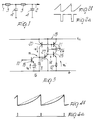
- figure 1 is the circuit diagram of a known solution;
- figures 2a and 2b illustrate the plot of two signals related to the known circuit of figure 1;
- figure 3 is an exemplifying circuit diagram of the invention; and
- figures 4a and 4b illustrate the plot of two signals related to the circuit according to the invention.
- With reference to figure 1, the circuit diagram of a known generator of periodic signals with exponential edges is illustrated therein.
- As can be seen, the circuit substantially comprises a ladder-like network having an
input pin 1 and an output pin 2 and having resistors 3 and capacitors 4. By applying on theinput 1 the control signal, illustrated in figure 2a, the output signal, on the pin 2, has the plot illustrated in figure 2b, from which it is apparent that, upon the arrival of a negative pulse on theinput 1, the capacitor 4 instantaneously discharge, while, when theinput 1 returns high, the capacitors begin to load with exponential behaviour. - Reference should now be made to figure 3, illustrating an example of the generator of periodic signals according to the invention.
- As can be seen, the generator comprises a capacitor 11 and a
resistor 12 supplied by a current mirror circuit indicated at 13, which feeds the capacitor and the resistor with mutually correlated currents. Between the capacitor 11 and theresistor 12 anamplifier circuit 14 is arranged, which maintains a proportionality, and precisely the equality, between the drop across the capacitor 11 and the drop across theresistor 12. The circuit, in its general structure, furthermore comprises a switch comprising here a transistor 15 the base terminal whereof constitutes the input 10 of the circuit to which pulses are fed which cause the conduction of the same transistor 15 and the discharge of the capacitor 11. - In detail, the transistor 15, of the NPN type, has its emitter terminal connected to the positive pole of a
constant voltage source 16 with value VR, while its collector terminal is connected to a terminal 17 of the capacitor 11, connected with the other terminal to the ground. Said terminal 17 is connected to thecurrent mirror circuit 13 formed by afirst transistor 20 and by asecond transistor 21, diode connected. In particular, the collector of thetransistor 20 is connected to the terminal 17, the emitter of thetransistor 20 is connected to the supply voltage, while its base is connected to the base of thetransistor 21, having the emitter also connected to the supply voltage and the collector connected to the collector of atransistor 25 which is part of theamplifier 14. In turn, thetransistor 25 has its emitter connected to a terminal of the resistor 12 (having the other terminal connected to the ground) and its base connected to the supply voltage through the resistor 26 and to the emitter of afurther transistor 27 constituting, with thetransistor 25, the amplifier. Thetransistor 27 is in turn connected with its base to the terminal 17 and with its collector to the ground. - The circuit illustrated in figure 3 operates as follows. The transistor 15 (receiving on the base 10 the signal illustrated in figure 4a) has the purpose of allowing the discharge of the capacitor 11 when its base is supplied with a pulse which causes said transistor to conduct. Accordingly, by virtue of the conduction of the transistor 15, the capacitor 11 discharges down to the voltage VR supplied by the
source 16. At the end of the pulse 4a, the transistor 15 is switched off, thus allowing charging of the capacitor 11 by means of the current ig supplied by thetransistor 20 of thecurrent mirror 13. Said current ig initially has the value VR/R, R being the resistance of theresistor 12. In fact, by virtue of the connection of thetransistors resistor 12 practically coincides with the voltage vc across the capacitor, while by virtue of themirror 13 having ratio 1:1, the current flowing in theresistor 12 is also supplied to the capacitor 11. Accordingly the capacitor 11 starts to charge with increasing current, the value whereof is a function of the voltage on the capacitor, fed to theresistor 12 by thecircuit 14. The voltage vc across the capacitor 11 increases until the new pulse on the input 10, which causes the new switching on of the transistor 15 and a new discharge of the capacitor 11. The equations which govern the system are as follows:

where from:
- Accordingly, during the charging period of the capacitor, across the same capacitor, and across the
resistor 12 connected so as to have the same voltage, an exponential voltage is present which can thus be used controlling amplitude modulation circuits of switching power supplies. - As can be seen from the preceding description, the invention fully achieves the proposed aim and objects. In fact a generator of signals with exponential edges has been provided which requires a single capacitor and which can be easily integrated. Said capacitor can be external or even integrated.
- The generator exploits a single pin (pin 10) of the integrated circuit of which it is part, therefore not causing the use of packages with greater dimensions, and therefore allowing the containment of the costs of the integrated circuit as a whole.
- The illustrated structure is furthermore extremely simple and therefore has per se reduced manufacture costs which allow its wide application.
- The invention thus conceived is susceptible to numerous modifications and variations, all within the scope of the inventive concept. In particular, though in the solution illustrated by way of example the current mirror operates so as to exactly mirror the current flowing in the
resistor 12 towards the capacitor 11, it is possible to also use other current mirrors supplying to the capacitor 11 a current in a given ratio, different from 1, with respect to the current flowing in the resistor, obtaining in this case only a current in the capacitor no longer equal but proportional to the voltage on the capacitor 11. - Furthermore, though the circuit formed by the
transistors - Furthermore all the details may be replaced with other technically equivalent ones.
- Where technical features mentioned in any claim are followed by reference signs, those reference signs have been included for the sole purpose of increasing the intelligibility of the claims and accordingly, such reference signs do not have any limiting effect on the scope of each element identified by way of example by such reference signs.
Claims (5)
- A generator of periodic signals with exponential edges, in particular for switch-mode power supplies, comprising:
at least one capacitive element (11) and a resistive element (12);
current source means (13) connected to said capacitive element (11) and to said resistive element (12) and supplying them with currents having mutually proportional amplitudes;
a switch device (15) connected in parallel to said capacitive element (11) for charging said capacitor element (11) according to a trigger signal and for allowing discharge of said capacitive element (11) therethrough; and
amplifier means (14), interposed between said capacitive element (11) and said resistive element (12), for maintaining the voltage drop on said resistive element (12) proportional to the voltage drop on said capacitive element (11), CHARACTERIZED IN THAT
said generator is an integrated circuit; in that
said switch device (15) is arranged such as to allow periodical switching by an external trigger signal; and in that
said amplifier means (14) comprises a first (27) and a second (25) transistor alternately of the PNP type and of the NPN type, said first transistor (27) being connected with its base terminal to a terminal (17) of said capacitive element (11), and said second transistor (25) being connected with its base terminal to the emitter terminal of said first transistor (27), with its emitter terminal to a terminal of said resistive element (12), and with its collector terminal to a terminal of said current source (13). - The circuit according to claim 1, characterized in that said current source means (13) comprises a current mirror circuit having a first terminal connected to said terminal (17) of said capacitive element (11) and a second terminal operatively connected to said terminal of said resistive element (12).
- The circuit according to claims 1 or 2, characterized in that said amplifier means (14) has unit gain.
- The circuit according to one or more of the preceding claims, characterized in that said switch device (15) comprises a third transistor connected with its respective emitter and collector terminals between said terminal (17) of said capacitive element (11) and a reference voltage point (VR), the base terminal (10) of said third transistor receiving control pulses for switching said third transistor and connecting said terminal (17) of said capacitive element (11) to said reference voltage point (VR).
- The circuit according to one or more of the preceding claims, characterized in that said third transistor is of the NPN type having its collector terminal connected to said terminal (17) of said capacitive element (11) and its emitter terminal connected to said reference potential point (VR).
Applications Claiming Priority (2)
| Application Number | Priority Date | Filing Date | Title |
|---|---|---|---|
| IT1949287 | 1987-02-25 | ||
| IT8719492A IT1215369B (en) | 1987-02-25 | 1987-02-25 | PERIODIC SIGNAL GENERATOR WITH EXPONENTIAL TREND, IN PARTICULAR FOR SWITCHING POWER SUPPLIES. |
Publications (3)
| Publication Number | Publication Date |
|---|---|
| EP0280170A2 EP0280170A2 (en) | 1988-08-31 |
| EP0280170A3 EP0280170A3 (en) | 1990-01-10 |
| EP0280170B1 true EP0280170B1 (en) | 1995-06-21 |
Family
ID=11158484
Family Applications (1)
| Application Number | Title | Priority Date | Filing Date |
|---|---|---|---|
| EP88102283A Expired - Lifetime EP0280170B1 (en) | 1987-02-25 | 1988-02-17 | Generator of periodic signals, in particular for switch-mode power supplies |
Country Status (5)
| Country | Link |
|---|---|
| US (1) | US4801816A (en) |
| EP (1) | EP0280170B1 (en) |
| JP (1) | JPS63227210A (en) |
| DE (1) | DE3854006T2 (en) |
| IT (1) | IT1215369B (en) |
Families Citing this family (16)
| Publication number | Priority date | Publication date | Assignee | Title |
|---|---|---|---|---|
| DE4017738A1 (en) * | 1990-06-01 | 1991-12-05 | Thomson Brandt Gmbh | COMPARATOR CIRCUIT FOR AN INTEGRATOR |
| US7330017B2 (en) * | 2004-01-29 | 2008-02-12 | Enpirion, Inc. | Driver for a power converter and a method of driving a switch thereof |
| US7521907B2 (en) | 2006-03-06 | 2009-04-21 | Enpirion, Inc. | Controller for a power converter and method of operating the same |
| US7893676B2 (en) * | 2006-07-20 | 2011-02-22 | Enpirion, Inc. | Driver for switch and a method of driving the same |
| US7948280B2 (en) * | 2006-10-20 | 2011-05-24 | Enpirion, Inc. | Controller including a sawtooth generator and method of operating the same |
| US7876080B2 (en) * | 2007-12-27 | 2011-01-25 | Enpirion, Inc. | Power converter with monotonic turn-on for pre-charged output capacitor |
| US8410769B2 (en) * | 2008-04-16 | 2013-04-02 | Enpirion, Inc. | Power converter with controller operable in selected modes of operation |
| US9246390B2 (en) | 2008-04-16 | 2016-01-26 | Enpirion, Inc. | Power converter with controller operable in selected modes of operation |
| US8692532B2 (en) * | 2008-04-16 | 2014-04-08 | Enpirion, Inc. | Power converter with controller operable in selected modes of operation |
| US8686698B2 (en) | 2008-04-16 | 2014-04-01 | Enpirion, Inc. | Power converter with controller operable in selected modes of operation |
| US8541991B2 (en) * | 2008-04-16 | 2013-09-24 | Enpirion, Inc. | Power converter with controller operable in selected modes of operation |
| US7679342B2 (en) * | 2008-04-16 | 2010-03-16 | Enpirion, Inc. | Power converter with power switch operable in controlled current mode |
| US9548714B2 (en) * | 2008-12-29 | 2017-01-17 | Altera Corporation | Power converter with a dynamically configurable controller and output filter |
| US8698463B2 (en) * | 2008-12-29 | 2014-04-15 | Enpirion, Inc. | Power converter with a dynamically configurable controller based on a power conversion mode |
| US8867295B2 (en) | 2010-12-17 | 2014-10-21 | Enpirion, Inc. | Power converter for a memory module |
| US9509217B2 (en) | 2015-04-20 | 2016-11-29 | Altera Corporation | Asymmetric power flow controller for a power converter and method of operating the same |
Family Cites Families (9)
| Publication number | Priority date | Publication date | Assignee | Title |
|---|---|---|---|---|
| US2983831A (en) * | 1959-02-24 | 1961-05-09 | Elcor Inc | Bootstrap circuits |
| US3569735A (en) * | 1968-09-24 | 1971-03-09 | Us Army | Constant amplitude sawtooth generator |
| SU474921A1 (en) * | 1973-01-02 | 1975-06-25 | Предприятие П/Я А-7438 | Sawtooth generator |
| US3831113A (en) * | 1973-06-01 | 1974-08-20 | Rca Corp | Relaxation oscillator |
| JPS50156348A (en) * | 1974-06-04 | 1975-12-17 | ||
| DE2511642C3 (en) * | 1975-03-17 | 1980-09-11 | Siemens Ag, 1000 Berlin Und 8000 Muenchen | Circuit arrangement for regulating the amplitude of a sawtooth generator |
| US4071776A (en) * | 1976-08-19 | 1978-01-31 | Rca Corporation | Sawtooth voltage generator for constant amplitude sawtooth waveform from varying frequency control signal |
| JPS56129423A (en) * | 1980-03-14 | 1981-10-09 | Sony Corp | Triangle wave generating circuit |
| JPS57326A (en) * | 1980-05-30 | 1982-01-05 | Suzuki Motor Co Ltd | Combustion chamber of internal combustion engine |
-
1987
- 1987-02-25 IT IT8719492A patent/IT1215369B/en active
-
1988
- 1988-02-17 EP EP88102283A patent/EP0280170B1/en not_active Expired - Lifetime
- 1988-02-17 DE DE3854006T patent/DE3854006T2/en not_active Expired - Fee Related
- 1988-02-22 US US07/158,811 patent/US4801816A/en not_active Expired - Lifetime
- 1988-02-23 JP JP63041806A patent/JPS63227210A/en active Pending
Non-Patent Citations (2)
| Title |
|---|
| J. Markus, "Modern Electronic Circuits Reference Manual", McGraw-Hill, 1980, page 432, circuit "Sine-Square-Triangle With Lin/Log Sweep" * |
| J. Markus, "Sourcebook of Electronic Circuits", McGraw-Hill, 1968, page 14, circuit "Broadband Impedance Transformer" * |
Also Published As
| Publication number | Publication date |
|---|---|
| US4801816A (en) | 1989-01-31 |
| IT8719492A0 (en) | 1987-02-25 |
| IT1215369B (en) | 1990-02-08 |
| EP0280170A2 (en) | 1988-08-31 |
| JPS63227210A (en) | 1988-09-21 |
| EP0280170A3 (en) | 1990-01-10 |
| DE3854006D1 (en) | 1995-07-27 |
| DE3854006T2 (en) | 1996-03-07 |
Similar Documents
| Publication | Publication Date | Title |
|---|---|---|
| EP0280170B1 (en) | Generator of periodic signals, in particular for switch-mode power supplies | |
| EP0580923A1 (en) | Circuit for detecting voltage variations in relation to a set value, for devices comprising errors amplifiers | |
| US3959714A (en) | Transient turn-on protection circuit for power supplies | |
| US4536662A (en) | Bidirectional constant current driving circuit | |
| GB2194405A (en) | Filter time constant adjuster | |
| US3934173A (en) | Circuit arrangement for generating a deflection current through a coil for vertical deflection in a display tube | |
| EP0012576A1 (en) | Coupling arrangement for a welding apparatus | |
| KR100231653B1 (en) | Mosfet switch matrix | |
| US4471289A (en) | Switching power supply circuit | |
| US5635868A (en) | Power transistor current limiter | |
| GB2027307A (en) | Transistor power amplifier protection circuit | |
| US4178558A (en) | DC Level clamping circuit | |
| EP0132863B1 (en) | Protection circuit | |
| US4501933A (en) | Transistor bridge voltage rectifier circuit | |
| JPS60263581A (en) | Drive circuit of deflecting power transistor | |
| US4016484A (en) | Solid state weld timer | |
| JPS61500347A (en) | Series transistor chip | |
| EP0651312B1 (en) | Drive circuit | |
| EP0410764A2 (en) | Comparator circuit | |
| JP2803151B2 (en) | Power supply | |
| JP3047012B2 (en) | Filter circuit | |
| EP0343553B1 (en) | Low voltage-controlled, stand-by electronic circuit with delayed switch off | |
| KR790000817B1 (en) | Circuit arrangement for generating a deflection current though a coil for vertical deflection in a coil for vertical deflection in a display tube | |
| US4024433A (en) | Circuit for generating a deflection current through a coil for the vertical deflection in a display tube | |
| US3143667A (en) | Monostable trigger arrangements |
Legal Events
| Date | Code | Title | Description |
|---|---|---|---|
| PUAI | Public reference made under article 153(3) epc to a published international application that has entered the european phase |
Free format text: ORIGINAL CODE: 0009012 |
|
| AK | Designated contracting states |
Kind code of ref document: A2 Designated state(s): DE FR GB NL |
|
| PUAL | Search report despatched |
Free format text: ORIGINAL CODE: 0009013 |
|
| AK | Designated contracting states |
Kind code of ref document: A3 Designated state(s): DE FR GB NL |
|
| RHK1 | Main classification (correction) |
Ipc: H03K 4/08 |
|
| 17P | Request for examination filed |
Effective date: 19900130 |
|
| 17Q | First examination report despatched |
Effective date: 19920227 |
|
| RAP1 | Party data changed (applicant data changed or rights of an application transferred) |
Owner name: SGS-THOMSON MICROELECTRONICS S.R.L. |
|
| GRAA | (expected) grant |
Free format text: ORIGINAL CODE: 0009210 |
|
| AK | Designated contracting states |
Kind code of ref document: B1 Designated state(s): DE FR GB NL |
|
| PG25 | Lapsed in a contracting state [announced via postgrant information from national office to epo] |
Ref country code: NL Free format text: LAPSE BECAUSE OF FAILURE TO SUBMIT A TRANSLATION OF THE DESCRIPTION OR TO PAY THE FEE WITHIN THE PRESCRIBED TIME-LIMIT Effective date: 19950621 |
|
| REF | Corresponds to: |
Ref document number: 3854006 Country of ref document: DE Date of ref document: 19950727 |
|
| ET | Fr: translation filed | ||
| NLV1 | Nl: lapsed or annulled due to failure to fulfill the requirements of art. 29p and 29m of the patents act | ||
| PLBE | No opposition filed within time limit |
Free format text: ORIGINAL CODE: 0009261 |
|
| STAA | Information on the status of an ep patent application or granted ep patent |
Free format text: STATUS: NO OPPOSITION FILED WITHIN TIME LIMIT |
|
| 26N | No opposition filed | ||
| REG | Reference to a national code |
Ref country code: FR Ref legal event code: D6 |
|
| REG | Reference to a national code |
Ref country code: GB Ref legal event code: IF02 |
|
| PGFP | Annual fee paid to national office [announced via postgrant information from national office to epo] |
Ref country code: GB Payment date: 20020802 Year of fee payment: 15 |
|
| PGFP | Annual fee paid to national office [announced via postgrant information from national office to epo] |
Ref country code: DE Payment date: 20020827 Year of fee payment: 15 |
|
| PGFP | Annual fee paid to national office [announced via postgrant information from national office to epo] |
Ref country code: FR Payment date: 20020828 Year of fee payment: 15 |
|
| PG25 | Lapsed in a contracting state [announced via postgrant information from national office to epo] |
Ref country code: GB Free format text: LAPSE BECAUSE OF NON-PAYMENT OF DUE FEES Effective date: 20030217 |
|
| PG25 | Lapsed in a contracting state [announced via postgrant information from national office to epo] |
Ref country code: DE Free format text: LAPSE BECAUSE OF NON-PAYMENT OF DUE FEES Effective date: 20030902 |
|
| GBPC | Gb: european patent ceased through non-payment of renewal fee | ||
| PG25 | Lapsed in a contracting state [announced via postgrant information from national office to epo] |
Ref country code: FR Free format text: LAPSE BECAUSE OF NON-PAYMENT OF DUE FEES Effective date: 20031031 |
|
| REG | Reference to a national code |
Ref country code: FR Ref legal event code: ST |
|
| APAH | Appeal reference modified |
Free format text: ORIGINAL CODE: EPIDOSCREFNO |