EP0279604B1 - Focused convection reflow soldering method and apparatus - Google Patents
Focused convection reflow soldering method and apparatus Download PDFInfo
- Publication number
- EP0279604B1 EP0279604B1 EP88301182A EP88301182A EP0279604B1 EP 0279604 B1 EP0279604 B1 EP 0279604B1 EP 88301182 A EP88301182 A EP 88301182A EP 88301182 A EP88301182 A EP 88301182A EP 0279604 B1 EP0279604 B1 EP 0279604B1
- Authority
- EP
- European Patent Office
- Prior art keywords
- components
- temperature
- board
- solder
- reflow
- Prior art date
- Legal status (The legal status is an assumption and is not a legal conclusion. Google has not performed a legal analysis and makes no representation as to the accuracy of the status listed.)
- Expired - Lifetime
Links
Images


Classifications
-
- H—ELECTRICITY
- H05—ELECTRIC TECHNIQUES NOT OTHERWISE PROVIDED FOR
- H05K—PRINTED CIRCUITS; CASINGS OR CONSTRUCTIONAL DETAILS OF ELECTRIC APPARATUS; MANUFACTURE OF ASSEMBLAGES OF ELECTRICAL COMPONENTS
- H05K3/00—Apparatus or processes for manufacturing printed circuits
- H05K3/30—Assembling printed circuits with electric components, e.g. with resistors
- H05K3/32—Assembling printed circuits with electric components, e.g. with resistors electrically connecting electric components or wires to printed circuits
- H05K3/34—Assembling printed circuits with electric components, e.g. with resistors electrically connecting electric components or wires to printed circuits by soldering
-
- B—PERFORMING OPERATIONS; TRANSPORTING
- B23—MACHINE TOOLS; METAL-WORKING NOT OTHERWISE PROVIDED FOR
- B23K—SOLDERING OR UNSOLDERING; WELDING; CLADDING OR PLATING BY SOLDERING OR WELDING; CUTTING BY APPLYING HEAT LOCALLY, e.g. FLAME CUTTING; WORKING BY LASER BEAM
- B23K1/00—Soldering, e.g. brazing, or unsoldering
- B23K1/012—Soldering with the use of hot gas
-
- B—PERFORMING OPERATIONS; TRANSPORTING
- B23—MACHINE TOOLS; METAL-WORKING NOT OTHERWISE PROVIDED FOR
- B23K—SOLDERING OR UNSOLDERING; WELDING; CLADDING OR PLATING BY SOLDERING OR WELDING; CUTTING BY APPLYING HEAT LOCALLY, e.g. FLAME CUTTING; WORKING BY LASER BEAM
- B23K1/00—Soldering, e.g. brazing, or unsoldering
- B23K1/005—Soldering by means of radiant energy
- B23K1/0053—Soldering by means of radiant energy soldering by means of infrared [IR]
-
- H—ELECTRICITY
- H05—ELECTRIC TECHNIQUES NOT OTHERWISE PROVIDED FOR
- H05K—PRINTED CIRCUITS; CASINGS OR CONSTRUCTIONAL DETAILS OF ELECTRIC APPARATUS; MANUFACTURE OF ASSEMBLAGES OF ELECTRICAL COMPONENTS
- H05K3/00—Apparatus or processes for manufacturing printed circuits
- H05K3/30—Assembling printed circuits with electric components, e.g. with resistors
- H05K3/32—Assembling printed circuits with electric components, e.g. with resistors electrically connecting electric components or wires to printed circuits
- H05K3/34—Assembling printed circuits with electric components, e.g. with resistors electrically connecting electric components or wires to printed circuits by soldering
- H05K3/3494—Heating processes for reflow soldering
-
- H—ELECTRICITY
- H05—ELECTRIC TECHNIQUES NOT OTHERWISE PROVIDED FOR
- H05K—PRINTED CIRCUITS; CASINGS OR CONSTRUCTIONAL DETAILS OF ELECTRIC APPARATUS; MANUFACTURE OF ASSEMBLAGES OF ELECTRICAL COMPONENTS
- H05K2203/00—Indexing scheme relating to apparatus or processes for manufacturing printed circuits covered by H05K3/00
- H05K2203/08—Treatments involving gases
- H05K2203/087—Using a reactive gas
Definitions
- This invention relates to systems for soldering electrical and electronic components onto substrate boards, and more particularly to an improved apparatus and method for mass reflow soldering electrical and electronic components to the top and/or bottom side surfaces of substrate circuit boards or the like in a single pass.
- the invention has particular application to soldering of surface mounted devices (SMDs) such as chips or the like to printed circuit boards and will be described in connection with such application.
- SMDs surface mounted devices
- solder surface mounted components to a circuit board using a solder cream or paste, or a solder preform or the like.
- the surface mounted components are loaded in position on a circuit board, together with suitable solder preforms or a solder cream or paste, and the circuit board and loaded components are heated to a temperature sufficient to reflow the solder. Heating the solder to reflow can be accomplished by baking the circuit board and components in a radiant furnace or the like.
- the circuit board and components may be immersed in a vapor heated to a temperature above the melting point of the solder, in accordance with the so-called vapor phase soldering or condensation soldering process. Such a process is described in U.S. Patent Nos.
- Radiant heating reflow soldering and vapor (condensation) soldering have achieved a certain degree of commercial acceptance although each technique has certain drawbacks. Radiant heating reflow soldering techniques have a tendency to overheat components which could cause damage to heat sensitive components, and radiant heating reflow soldering techniques are susceptible to line-of-sight shadowing and/or thermal absorption differences due to different optical and/or mass characteristics of components and thus may not be entirely satisfactory for many applications. And, the fluid used to create the vapor for condensation soldering is quite expensive, and the thermal decomposition products of the fluid produced are dangerous to health. Moreover, both radiant heating and condensation soldering techniques require relatively long warmup and product changeover lead times.
- a circuit board containing components populating both top and bottom surfaces of the board is first subjected to a first mass soldering operation in which the bottom side surfaces of the board and components thereon are passed in contact with a body of molten solder as by passing through the crest of a standing solder wave.
- the first mass soldering operation reportedly also imparts substantial heat energy to the board, which heat energy is conducted through to the top side surface of the board. Additional heat energy then is supplied to the top side surface of the board to reflow preapplied solder cream or paste or solder preforms on the board top side surface.
- the Comerford patented soldering system comprises a fluxing station wherein flux may be applied to the bottom surface of the circuit board; a preheater station wherein the flux is activated and the board prepared for soldering; a first mass soldering station wherein the bottom side surface of the printed circuit board may be brought into contact with a pool of molten solder; and a second mass soldering station wherein preapplied solder cream or paste or solder preforms on the top side surface of the printed circuit board may be heated to reflow.
- the first soldering station comprises a wave soldering assembly consisting of two wave-forming solder sumps including a first nozzle for forming a bidirectional wave and a second nozzle for forming a second substantially unnidirectional wave
- the second mass soldering station comprises a convection heating assembly consisting of one or more heated nozzles for directing heated fluid streams substantially vertically downwardly onto the top side surface of the board.
- the heated fluid comprises heated air.
- Completing the Comerford patented apparatus is means for transporting the circuit boards to be soldered in-line in timed sequence between the first mass soldering station and the second mass soldering (reflow) station.
- the Comerford patented mass soldering system has been incorporated into mass soldering systems available from Hollis Automation, Inc. and is considered to constitute a significant advance and contribution to the art of mass soldering. And, while the above described Comerford patented mass soldering system can be used for mass soldering circuit boards containing only surface mounted components, the Comerford patented mass soldering system is overly complex for soldering circuit boards having no leaded components.
- the invention provides apparatus as defined in Claim 1, and a method as defined in Claim 6, of which in each case the pre-characterising part acknowledges the features disclosed in the Comerford patent.
- component refers to so-called surface mounted components or devices such as chip components as well as carriers therefor.
- component lead refers to that part of the metal conductor of an electrical or electronic component that is joined to the printed circuit board pattern.
- laminate refers to that part of metallic pattern on the printed circuit board to which a component or component lead is joined by solder
- top side surface and bottom side surface as used herein with reference to the circuit board are meant simply to refer to the opposed board surfaces of the circuit board; the terms “top” and “bottom” respectively denote spatial orientation of the circuit board only as it is heing processed in the soldering apparatus in accordance with the present invention.
- mass reflow soldering is intended to refer to the soldering technique in which solder connections are made by reflow of preapplied solder preforms, or solder cream paste on a circuit board.
- forced convection as used herein with reference to the convection heating means is meant to differentiate driven convective heating means as employed in the invention from natural convection movement.
- relatively low velocity and “relatively high velocity” as used herein with reference to the convection heating means are employed as relative terms.
- the system has means for transporting the circuit boards to be soldered in-line in timed sequence between the first (preheating) zone and the second (reflow) zone.
- a printed circuit board 14 is loaded at an insertion station (not shown) with a plurality of electrical and electronic components 18 on the top side surface 20 of the board.
- the board 14 comprises an insulated wiring board having one or more printed metallic conductors (not shown) on the board top side surface 20.
- Components 18 are temporarily affixed in known manner in suitable locations on the board top side surface by means of a solder paste or the like applied to the component leads and circuit lands. If desired components 18 also may be affixed to the circuit board by means of an epoxy adhesive or the like applied to the component bodies.
- Reflow apparatus 30' is divided into a preheat zone comprising plurality of functional heat management zones, indicated by the Roman Numerals I to IV which correspond to the heat management zones and description temperature graph of Fig. 4 as will be described hereinbelow, and a reflow zone indicated by Roman Numeral V.
- dividing the reflow apparatus 30' into a plurality of heat management zones permits controlled heating whereby to provide a desired temperature ramping, and stabilization of temperature whereby to avoid overheating and/or underheating of individual components.
- heating is primarily effected by means of an infra-red (IR) heat source, with little or no supplemental convective gas heating.
- IR heating is supplemented with a relatively low velocity hot gas convective heating whereas to maintain the increasing temperature ramp, while levelling, in part, the temperature differences resulting from IR absorption rates due to reflectivity, shadowing and nesting of components relative to one another.
- preheating Zone III heating is primarily achieved by means of relatively low velocity heated gas convective heating with IR heating optional.
- Preheating Zone III contributes to the increasing temperature ramp, while further levelling component temperature differences and achieving an efficiency balance between component temperature to air temperature.
- Preheating Zone IV comprises additional relatively low velocity hot gas convection heating means for heating the circuit board and components to just below the reflow of the temperature of the solder.
- heating is achieved by means of one or a plurality of hot gas knives which produce a relatively high velocity convective gas stream for heating the components and circuit board top side surface to a temperature above the reflow temperature of the solder.
- the apparatus comprises an electrically powered, variable speed blower 38 connected between its inlet pipe 40 and an air supply plenum 42 which, in turn, is connected to supply air to various smaller plenums and nozzles to be described in detail below.
- a control system 44 is connected to receive temperature inputs from sensors within the enclosure 46 of reflow station 30' as typified by the sensor indicated at 48.
- Temperature sensors will be located within the individual plenums. Temperature sensors and the types of control systems employing them are well known in the art and are available commercially and, therefore, in the interest of simplicity and avoiding redundancy herein, they will not be described in detail.
- Control system 44 is operatively connected to control the speed of the blower 38, a damper 50 controlling the mixture of outside air 52 and recirculated enclosure air 54 from within the enclosure 46 being pumped to the plenum 42, one or more dampers or valves (not shown) for controlling the volume and temperature of heated air directed to the various air outlet nozzles as will be described in detail hereinafter, and (optionally) an in-line heater 56 for adding heat to the system when the enclosure air 54 alone is of insufficient temperature to affect the desired objectives.
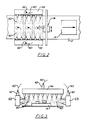
- a typical arrangement for preheating Zones I, II and III is shown in top view in Fig. 2 and in end view in Fig. 3.
- Pairs of spaced plenums 58A, 58B, 58C are disposed above and below conveyor 12 carrying the printed circuit boards 14 thereon.
- Plenums 58A, 58B, 58C are connected to receive convection air 60 through inlets 59 from the air supply plenum 42 and contain a plurality of upwardly and downwardly facing nozzles 61 through which the heated air 60 emerges to flow across the broad surfaces of a printed circuit board 14 passing therebetween.
- nozzles 61 are disposed between banks of spaced IR heaters 28A, 28B, 28C.
- the latter preferably comprise quartz-lamp, high mass type heaters as are conventionally employed as IR preheaters in mass soldering systems.
- side plenums 63 are disposed on opposite sides of the conveyor 12 and are also connected to receive convection air 60 through inlets 62 from the heated air supply plenum 42. Heated air may he recaptured and recycled by suitable return means (not shown) adjacent the ends of enclosure 46. Alternatively, the side plenums may be plumbed as returns.
- the preheating Zone comprises six separately controlled banks of IR heaters disposed three banks above and three banks below the travel path of the circuit boards.
- plenums 58A, 58B, 58C and 63 are arranged so that the air flow and temperature of air emanating from these plenums may be separately controlled.
- the temperature of the air emanating from the first in-line plenums 58A and 63A is adjusted to run slightly cooler than the temperatures expected to be reached by the circuit board and components so as to force temperature leveling.
- the temperature of the air emanating from the plenums may be at or slightly above the preheat target temperature for the board and components.
- Low profile components 66 are shadowed by higher profile components 68 from receiving the IR radiation indicated by the lines 70.
- the convection air 60 as indicated by the dashed lines so numbered, passes over, under, around and through the components 66, 68 picking up heat from and cooling the overheated, radiating components and transferring the heat to the cooler, underheated components.
- the overall effect is a stabilizing of the entire temperature profile of the board 14 and components 66, 68 to a temperature approximating that of the temperature of the air 60.
- a desired temperature profile can be achieved.
- one or more adjustable nozzle assemblies 74 connected to receive heated air 60 optionally can be provided for selectively directing air flow against particularly troublesome components during a specific soldering operation.
- selected components could be selectively cooled or heated, whereby to achieve a more level and consistent temperature of the various components on the board, thus compensating for the individual components' different IR absorption rates due to reflectivity, shadowing and nesting.
- the apparatus for each of preheating Zones I, II and IV could be separately pumped, mixed and/or heated under separate temperature control as may be required for the particular operation.
- the hot air knife 76 of preheating Zone III preferably produces a higher velocity stream of heated air 60 than that employed in preheating Zones I, II and IV, and may also incorporate a separate heater within its supply plenum 78, if desired.
- Zone V comprises the reflow section of the soldering system made in accordance with the present invention.
- Zone V comprises three separately controlled hot air knives 80, 82 and 84, similar in construction to the hot air knives taught in U.S. Patent No. 4,410,126 to Harold T. O'Rourke, assigned to the common assignee.
- Hot air knives 80, 82 and 84 are operated at higher temperature and flow rates than the hot air nozzles in preheating Zones I to IV previously described.
- the hot air knives in preheater Zone V are designed and operated primarily to input sufficient additional heat to substantially uniformly raise the temperature of the board and components sufficiently high to reflow the solder cream or paste and/or solder preforms on the board.
- the air employed in preheating Zones I to IV generally may be at a temperature ranging from about ambient to about 177°C 350°F
- the hot air employed in reflow Zone V should be at a temperature in the range of about 180°-480°C (about 350°F to about 900°F), or higher.
- the air employed in preheating Zones I to IV may in certain applications be at somewhat higher temperatures, e.g. up to about 260°C (500°F) or even higher. However, due to the relatively low air flow rates employed in preheating Zones I to IV the heat input from operating at such higher temperatures generally will not be sufficient to effect reflow in Zones I to IV. Air flow rates may be adjusted emperically in Zones I to IV to achieve the desired temperature leveling and in Zone V to achieve the desired reflow. Actual flow rates depend on a number of variables including target temperatures, heat input from IR heaters, number, size, configuration and spacing of air nozzles or air knives, ambient temperatures and work load.
- thermal levelling of the present invention can improve the process throughout from the normal 470-710 cm3 per second (1.0 to 1.5 fpm) for a pure IR reflow system to at least 1200-1650 cm3 per second (2.5 to 3.5 fpm). Moreover, as can be readily appreciated from the description hereinbefore, the thermal levelling accomplished in the preheating Zones I to IV virtually eliminates the possibility of component or board damage due to thermal shock and/or overheating.
- the heated convective gas in the preheating zone or zones is flooded or flowed, at relatively low velocity, in conjunction with the infra-red preheating.
- the low pressure, low velocity flow of heated convective air produces an improved distribution of component and board surface temperature.
- the convective gas flow in preheating Zones I to IV should be flowed over the circuit board and components at a velocity sufficient to more evenly distribute surface temperatures, but not so high as to disturb the components. The convective air flow thus lowers the temperature of high IR absorption components and raises the temperature of lower IR absorption components.
- a feature and advantage of the present invention is that the system utilizes normally wasted thermal heat by re-circulating IR derived heat within the system enclosure. However, should the recirculated air reach a steady state higher than desired range for preheat or reflow soldering, ambient makeup air readily can be added through a thermistor controlled dampened inlet. Additional heat can be provided, if required, by a heat source within the air manifold.
- the reflow Zone V comprises one or a plurality of heated air knives, fluid jets, slots, nozzles or the like indicated at 80, 82, 84, from which a relatively high pressure heated fluid stream such as air is directed to the top side surface of the board.
- a single air knife can be used under certain circumstances; however, it has been found that a minimum of two and preferably three air knives are preferred in order to achieve desired enhancement of thermal levelling, and at the same time achieve good solder reflow.
- a plurality of hot air knives is employed in reflow Zone V, it is found that operating the first hot air knife just about at the normal reflow temperature of the solder or even slightly below the reflow temperature may further enhance thermal levelling.
- the target operating temperatures also will vary depending on the particular solder alloy employed.
- conveyor system 12 is of conventional construction and typically comprises a pair of spaced conveyor rails and suitable drive means (not shown).
- conveyor system 12 operates substantially in the horizontal plane so that boards being processed are carried by conveyor 12 along a substantially horizontal travel path. Operating in the horizontal mode minimizes possible problems of component shifting on the board top surface and also simplifies loading and unloading transitions.
- a particular feature and advantage of the present invention is the ability to create substantially uniform heating of the component surface temperature of a circuit board in a reflow process independent of temperature and color characteristics of components' reflectivity, shadowing and nesting, and the like, thus providing more uniform heating and soldering of the components and eliminating possible thermal damage to individual components.
- Other features and advantages of the present invention include enhanced energy efficiency due to capture and recirculation of IR heated air, and elimination of expensive and potentially dangerous chemicals as are required for vapor reflow soldering systems.
- the present invention permits emergency shutdown under conditions which would eliminate or at least substantially reduce the possibility of damage to boards, permits easy and rapid maintenance and repair, and permits rapid adjustment in overall system temperatures so that warm-up and product changeovers may be accomplished quickly and easily.
- the rapidity of the reflow accomplished by the focused convection heated air in accordance with the present invention minimizes intermetallic growth in the joints, since exposure times at reflow temperatures are extremely short.
- IR heaters could be included in the reflow Zone V for providing additional heat input.
- the combination of IR and convective heating also may be advantageously employed for temperature leveling in the mass soldering system of Comerford, U.S. Patent 4,600,137.
- forced cooling means may be included immediately following the reflow Zone V.
Landscapes
- Engineering & Computer Science (AREA)
- Mechanical Engineering (AREA)
- Manufacturing & Machinery (AREA)
- Microelectronics & Electronic Packaging (AREA)
- Electric Connection Of Electric Components To Printed Circuits (AREA)
- Manufacturing Of Electrical Connectors (AREA)
- Lining Or Joining Of Plastics Or The Like (AREA)
Abstract
Description
- This invention relates to systems for soldering electrical and electronic components onto substrate boards, and more particularly to an improved apparatus and method for mass reflow soldering electrical and electronic components to the top and/or bottom side surfaces of substrate circuit boards or the like in a single pass. The invention has particular application to soldering of surface mounted devices (SMDs) such as chips or the like to printed circuit boards and will be described in connection with such application.
- In response to recent demands for compact electronic appliances and instruments, there has been a tendency to use small, thin chip type electronic parts, i.e. surface mounted components or devices for mounting on printed circuit boards in place of conventional, discrete type, leaded components. The advent of surface mounted component technology has afforded striking new levels of efficiency to the circuit board designer and, at the same time, has posed new challenges for the manufacturing engineer.
- Various techniques have been proposed by the art for mass soldering surface mounted components (and/or carriers therefor) to a circuit board. One technique involves fixturing the components to a circuit board, e.g., using an epoxy or the like, inverting the board, and then engaging the inverted board and fixtured components with molten solder by passing the inverted board and fixtured components in contact with a body of molten solder as, for example, through the crest of a standing solder wave. Such a process is described in U.S. Patent No. 4,465,219 to Kenshi Kondo.
- It has also been proposed to solder surface mounted components to a circuit board using a solder cream or paste, or a solder preform or the like. In such prior art technique, the surface mounted components are loaded in position on a circuit board, together with suitable solder preforms or a solder cream or paste, and the circuit board and loaded components are heated to a temperature sufficient to reflow the solder. Heating the solder to reflow can be accomplished by baking the circuit board and components in a radiant furnace or the like. Alternatively, the circuit board and components may be immersed in a vapor heated to a temperature above the melting point of the solder, in accordance with the so-called vapor phase soldering or condensation soldering process. Such a process is described in U.S. Patent Nos. 3,866,307 and 4,321,031, which are given as exemplary. Radiant heating reflow soldering and vapor (condensation) soldering have achieved a certain degree of commercial acceptance although each technique has certain drawbacks. Radiant heating reflow soldering techniques have a tendency to overheat components which could cause damage to heat sensitive components, and radiant heating reflow soldering techniques are susceptible to line-of-sight shadowing and/or thermal absorption differences due to different optical and/or mass characteristics of components and thus may not be entirely satisfactory for many applications. And, the fluid used to create the vapor for condensation soldering is quite expensive, and the thermal decomposition products of the fluid produced are dangerous to health. Moreover, both radiant heating and condensation soldering techniques require relatively long warmup and product changeover lead times.
- U.S. Patent No. 4,600,137 to Matthias F. Comerford entitled METHOD AND APPARATUS FOR MASS SOLDERING WITH SUBSEQUENT REFLOW SOLDERING and assigned to the common assignee of this application discloses an improved mass soldering system which overcomes the aforesaid and other disadvantages of the prior art and also permits mass soldering components to both sides of a printed circuit board in a single pass. More particularly, in accordance with the Comerford patented soldering system, a circuit board containing components populating both top and bottom surfaces of the board is first subjected to a first mass soldering operation in which the bottom side surfaces of the board and components thereon are passed in contact with a body of molten solder as by passing through the crest of a standing solder wave. The first mass soldering operation reportedly also imparts substantial heat energy to the board, which heat energy is conducted through to the top side surface of the board. Additional heat energy then is supplied to the top side surface of the board to reflow preapplied solder cream or paste or solder preforms on the board top side surface. The Comerford patented soldering system comprises a fluxing station wherein flux may be applied to the bottom surface of the circuit board; a preheater station wherein the flux is activated and the board prepared for soldering; a first mass soldering station wherein the bottom side surface of the printed circuit board may be brought into contact with a pool of molten solder; and a second mass soldering station wherein preapplied solder cream or paste or solder preforms on the top side surface of the printed circuit board may be heated to reflow. In a preferred embodiment of the Comerford patented soldering system the first soldering station comprises a wave soldering assembly consisting of two wave-forming solder sumps including a first nozzle for forming a bidirectional wave and a second nozzle for forming a second substantially unnidirectional wave, and the second mass soldering station comprises a convection heating assembly consisting of one or more heated nozzles for directing heated fluid streams substantially vertically downwardly onto the top side surface of the board. In a particularly preferred embodiment of the invention the heated fluid comprises heated air. Completing the Comerford patented apparatus is means for transporting the circuit boards to be soldered in-line in timed sequence between the first mass soldering station and the second mass soldering (reflow) station.
- It is also mentioned in the Comerford patent that radiant and convective heating means may be combined.
- The Comerford patented mass soldering system has been incorporated into mass soldering systems available from Hollis Automation, Inc. and is considered to constitute a significant advance and contribution to the art of mass soldering. And, while the above described Comerford patented mass soldering system can be used for mass soldering circuit boards containing only surface mounted components, the Comerford patented mass soldering system is overly complex for soldering circuit boards having no leaded components.
- We acknowledge that it is known from US-A-3515330 to provide a continuous flow mass pin-to-board hot air soldering device, using thermostatic control of temperature in a heating zone using convection heating.
- The invention provides apparatus as defined in Claim 1, and a method as defined in Claim 6, of which in each case the pre-characterising part acknowledges the features disclosed in the Comerford patent.
- In the following detailed description of the invention, the term "component" refers to so-called surface mounted components or devices such as chip components as well as carriers therefor. The term "component lead" refers to that part of the metal conductor of an electrical or electronic component that is joined to the printed circuit board pattern. The term "land" as used herein refers to that part of metallic pattern on the printed circuit board to which a component or component lead is joined by solder, the terms "top side surface" and "bottom side surface" as used herein with reference to the circuit board are meant simply to refer to the opposed board surfaces of the circuit board; the terms "top" and "bottom" respectively denote spatial orientation of the circuit board only as it is heing processed in the soldering apparatus in accordance with the present invention. The term "mass reflow soldering" is intended to refer to the soldering technique in which solder connections are made by reflow of preapplied solder preforms, or solder cream paste on a circuit board. The term "forced convection" as used herein with reference to the convection heating means is meant to differentiate driven convective heating means as employed in the invention from natural convection movement. The terms "relatively low velocity" and "relatively high velocity" as used herein with reference to the convection heating means are employed as relative terms.
- In a preferred embodiment, the system has means for transporting the circuit boards to be soldered in-line in timed sequence between the first (preheating) zone and the second (reflow) zone.
- For a fuller understanding of the object of the present invention, reference should be had to the following detailed description of a preferred embodiment, by way of example only, taken in connection with the accompanying drawings in which like numerals depict like parts, and in which:
- Fig. 1 is a side elevational view, diagrammatically illustrating a mass soldering system embodying the present invention;
- Fig. 2 is a top plan view of a portion of the mass soldering system shown in Fig. 1;
- Fig. 3 is an end view of the mass soldering system shown in Fig. 1;
- Fig. 4 is a graph illustrating measurements representing time/temperature profiles of the top side surface of circuit boards passing through the mass soldering system of Figs. 1-3 operating in accordance with the teachings of the present invention; and
- Fig. 5 is an enlarged simplified drawing illustrating the heating effects achieved in accordance with the teachings of the present invention.
- Referring to Figs. 1 to 3, a printed
circuit board 14 is loaded at an insertion station (not shown) with a plurality of electrical andelectronic components 18 on the top side surface 20 of the board. For convenience of illustration, the components are shown loaded only on the top side surface of the board. However, as will become clear from the description following, the invention is equally useful for reflow soldering components to the top and/or bottom side surfaces of a circuit board. Theboard 14 comprises an insulated wiring board having one or more printed metallic conductors (not shown) on the board top side surface 20.Components 18 are temporarily affixed in known manner in suitable locations on the board top side surface by means of a solder paste or the like applied to the component leads and circuit lands. Ifdesired components 18 also may be affixed to the circuit board by means of an epoxy adhesive or the like applied to the component bodies. - The component carrying board is then loaded on a
conveyor 12 for travel through the solder reflow apparatus in accordance with the present invention as indicated generally at 30'. Reflow apparatus 30' is divided into a preheat zone comprising plurality of functional heat management zones, indicated by the Roman Numerals I to IV which correspond to the heat management zones and description temperature graph of Fig. 4 as will be described hereinbelow, and a reflow zone indicated by Roman Numeral V. As will be described below, dividing the reflow apparatus 30' into a plurality of heat management zones permits controlled heating whereby to provide a desired temperature ramping, and stabilization of temperature whereby to avoid overheating and/or underheating of individual components. - More particularly, with reference to Figs. 1 and 4, and as will be further described in detail hereinafter, in preheating Zone I, heating is primarily effected by means of an infra-red (IR) heat source, with little or no supplemental convective gas heating. In preheating Zone II, IR heating is supplemented with a relatively low velocity hot gas convective heating whereas to maintain the increasing temperature ramp, while levelling, in part, the temperature differences resulting from IR absorption rates due to reflectivity, shadowing and nesting of components relative to one another. In preheating Zone III, heating is primarily achieved by means of relatively low velocity heated gas convective heating with IR heating optional. Preheating Zone III contributes to the increasing temperature ramp, while further levelling component temperature differences and achieving an efficiency balance between component temperature to air temperature. Preheating Zone IV comprises additional relatively low velocity hot gas convection heating means for heating the circuit board and components to just below the reflow of the temperature of the solder. Finally, in reflow Zone V, heating is achieved by means of one or a plurality of hot gas knives which produce a relatively high velocity convective gas stream for heating the components and circuit board top side surface to a temperature above the reflow temperature of the solder.
- Turning now to Figs. 1 to 3 of the drawings, the heat management zones as provided by the apparatus of the present invention will now be discussed in detail. While in certain instances fluids other than air may be used as the hot gas working fluid for the convection heating and should be considered as being within the scope and spirit of the present invention, the preferred working fluid generally is air. More particularly, the apparatus comprises an electrically powered,
variable speed blower 38 connected between itsinlet pipe 40 and anair supply plenum 42 which, in turn, is connected to supply air to various smaller plenums and nozzles to be described in detail below. In a preferred embodiment of the invention, a control system 44 is connected to receive temperature inputs from sensors within theenclosure 46 of reflow station 30' as typified by the sensor indicated at 48. Preferably temperature sensors will be located within the individual plenums. Temperature sensors and the types of control systems employing them are well known in the art and are available commercially and, therefore, in the interest of simplicity and avoiding redundancy herein, they will not be described in detail. - Control system 44 is operatively connected to control the speed of the
blower 38, adamper 50 controlling the mixture ofoutside air 52 and recirculatedenclosure air 54 from within theenclosure 46 being pumped to theplenum 42, one or more dampers or valves (not shown) for controlling the volume and temperature of heated air directed to the various air outlet nozzles as will be described in detail hereinafter, and (optionally) an in-line heater 56 for adding heat to the system when theenclosure air 54 alone is of insufficient temperature to affect the desired objectives. - A typical arrangement for preheating Zones I, II and III is shown in top view in Fig. 2 and in end view in Fig. 3. Pairs of
spaced plenums conveyor 12 carrying the printedcircuit boards 14 thereon.Plenums convection air 60 throughinlets 59 from theair supply plenum 42 and contain a plurality of upwardly and downwardly facingnozzles 61 through which theheated air 60 emerges to flow across the broad surfaces of a printedcircuit board 14 passing therebetween. Preferably, but not necessarily,nozzles 61 are disposed between banks of spacedIR heaters side plenums 63 , are disposed on opposite sides of theconveyor 12 and are also connected to receiveconvection air 60 throughinlets 62 from the heatedair supply plenum 42. Heated air may he recaptured and recycled by suitable return means (not shown) adjacent the ends ofenclosure 46. Alternatively, the side plenums may be plumbed as returns. - One or more of the banks of
IR heaters manner plenums line plenums 58A and 63A is adjusted to run slightly cooler than the temperatures expected to be reached by the circuit board and components so as to force temperature leveling. In preheating Zones II, III and IV, the temperature of the air emanating from the plenums may be at or slightly above the preheat target temperature for the board and components. - The effect of this arrangement is illustrated in Fig. 5.
Low profile components 66 are shadowed byhigher profile components 68 from receiving the IR radiation indicated by the lines 70. Assuming that one of the shadowingcomponents 68 is absorbing the IR radiation and re-radiating heat as indicated by the wave lines 72, theconvection air 60 as indicated by the dashed lines so numbered, passes over, under, around and through thecomponents board 14 andcomponents air 60. Thus, by controlling the speed of theblower 38 and/or the mixture ofoutside air 52 and inside air 54 (and in-line heater 56 as necessary), a desired temperature profile can be achieved. - As shown in Fig. 2, one or more
adjustable nozzle assemblies 74, connected to receiveheated air 60 optionally can be provided for selectively directing air flow against particularly troublesome components during a specific soldering operation. In this manner, selected components could be selectively cooled or heated, whereby to achieve a more level and consistent temperature of the various components on the board, thus compensating for the individual components' different IR absorption rates due to reflectivity, shadowing and nesting. As those skilled in the art will appreciate, while not specifically shown nor described herein for the sake of simplicity, the apparatus for each of preheating Zones I, II and IV could be separately pumped, mixed and/or heated under separate temperature control as may be required for the particular operation. - The
hot air knife 76 of preheating Zone III preferably produces a higher velocity stream ofheated air 60 than that employed in preheating Zones I, II and IV, and may also incorporate a separate heater within itssupply plenum 78, if desired. - Zone V comprises the reflow section of the soldering system made in accordance with the present invention. In the preferred embodiment of the invention Zone V comprises three separately controlled
hot air knives Hot air knives - The air employed in preheating Zones I to IV may in certain applications be at somewhat higher temperatures, e.g. up to about 260°C (500°F) or even higher. However, due to the relatively low air flow rates employed in preheating Zones I to IV the heat input from operating at such higher temperatures generally will not be sufficient to effect reflow in Zones I to IV. Air flow rates may be adjusted emperically in Zones I to IV to achieve the desired temperature leveling and in Zone V to achieve the desired reflow. Actual flow rates depend on a number of variables including target temperatures, heat input from IR heaters, number, size, configuration and spacing of air nozzles or air knives, ambient temperatures and work load. Generally, for the purposes of this invention good results have been achieved operating the relatively low velocity convection heating means at air flow rates in the range of about 3m to 15m per second (about 10 to about 50 feet per second) as measured at the air nozzle air knife outlet, and operating the relatively high velocity convection heating means at air flow rates above about 15m per second (50 feet per second) as measured at the air nozzle or air knife outlet.
- Initial tests indicate that the thermal levelling of the present invention can improve the process throughout from the normal 470-710 cm³ per second (1.0 to 1.5 fpm) for a pure IR reflow system to at least 1200-1650 cm³ per second (2.5 to 3.5 fpm). Moreover, as can be readily appreciated from the description hereinbefore, the thermal levelling accomplished in the preheating Zones I to IV virtually eliminates the possibility of component or board damage due to thermal shock and/or overheating.
- In order to achieve better heating uniformity of the components and circuit board top surface, the heated convective gas in the preheating zone or zones is flooded or flowed, at relatively low velocity, in conjunction with the infra-red preheating. The low pressure, low velocity flow of heated convective air produces an improved distribution of component and board surface temperature. Obviously, the convective gas flow in preheating Zones I to IV should be flowed over the circuit board and components at a velocity sufficient to more evenly distribute surface temperatures, but not so high as to disturb the components. The convective air flow thus lowers the temperature of high IR absorption components and raises the temperature of lower IR absorption components.
- A feature and advantage of the present invention is that the system utilizes normally wasted thermal heat by re-circulating IR derived heat within the system enclosure. However, should the recirculated air reach a steady state higher than desired range for preheat or reflow soldering, ambient makeup air readily can be added through a thermistor controlled dampened inlet. Additional heat can be provided, if required, by a heat source within the air manifold.
- As noted supra, the reflow Zone V comprises one or a plurality of heated air knives, fluid jets, slots, nozzles or the like indicated at 80, 82, 84, from which a relatively high pressure heated fluid stream such as air is directed to the top side surface of the board. A single air knife can be used under certain circumstances; however, it has been found that a minimum of two and preferably three air knives are preferred in order to achieve desired enhancement of thermal levelling, and at the same time achieve good solder reflow. Moreover, when a plurality of hot air knives is employed in reflow Zone V, it is found that operating the first hot air knife just about at the normal reflow temperature of the solder or even slightly below the reflow temperature may further enhance thermal levelling. In such case the remaining air knife or
air knives hot air knives - The target operating temperatures also will vary depending on the particular solder alloy employed.
- Completing the apparatus is a conveyor system indicated generally at 12. The latter is of conventional construction and typically comprises a pair of spaced conveyor rails and suitable drive means (not shown). Preferably
conveyor system 12 operates substantially in the horizontal plane so that boards being processed are carried byconveyor 12 along a substantially horizontal travel path. Operating in the horizontal mode minimizes possible problems of component shifting on the board top surface and also simplifies loading and unloading transitions. - A particular feature and advantage of the present invention is the ability to create substantially uniform heating of the component surface temperature of a circuit board in a reflow process independent of temperature and color characteristics of components' reflectivity, shadowing and nesting, and the like, thus providing more uniform heating and soldering of the components and eliminating possible thermal damage to individual components. Other features and advantages of the present invention include enhanced energy efficiency due to capture and recirculation of IR heated air, and elimination of expensive and potentially dangerous chemicals as are required for vapor reflow soldering systems. Additionally, the present invention permits emergency shutdown under conditions which would eliminate or at least substantially reduce the possibility of damage to boards, permits easy and rapid maintenance and repair, and permits rapid adjustment in overall system temperatures so that warm-up and product changeovers may be accomplished quickly and easily. Moreover, the rapidity of the reflow accomplished by the focused convection heated air in accordance with the present invention minimizes intermetallic growth in the joints, since exposure times at reflow temperatures are extremely short.
- Various changes may be made, for example IR heaters could be included in the reflow Zone V for providing additional heat input. The combination of IR and convective heating also may be advantageously employed for temperature leveling in the mass soldering system of Comerford, U.S. Patent 4,600,137. Also, if desired, forced cooling means may be included immediately following the reflow Zone V.
Claims (10)
- Solder reflow apparatus for mass joining with solder electrical and electronic components positioned on at least one surface of a circuit board (20), and comprising in combination a plurality of preheating zones (I,II,III,IV) and a solder reflow zone (V), and means (12) for conveying the board (20) successively through those zones, the preheating zones consisting of a combination of IR heating means (28) and convective heating means (58) for heating said board (20) and components to just below the solder reflow temperature, and the solder reflow zone comprising convective heating means (80-84) for directing heated gas stream across said board (20) and components to raise the temperature of said board (20) and components sufficient to reflow solder preforms and/or solder paste or cream thereon;
characterised in that each preheating zone (I,II,III,IV) has heating means at least on the same side of the circuit board as the, or one of the, convective heating means (80-84) of the solder reflow zone, so that the said surface of the circuit board may be heated directly from all preheating and solder reflow zones (I to V), and in that the apparatus has a control system (44) for the convective heating means (58) responsive to the temperature within said enclosure to set the flow rate and temperature of the heated gas stream at each corresponding preheating zone (I,II,IV) to predetermined levels so as to adjust the heat input to each preheating zone to provide a predetermined steady rate of temperature increase of the board (20) and the components as they are conveyed through that preheating zone, whereby the temperature is ramped as a function of time over successive preheating zones, thereby avoiding overheating of individual components, but equalising the temperature differences between portions of the board (20) and individual components. - Solder reflow apparatus according to claim 1, characterised in that said preheating zones (I,II,III,IV) are contained within a gas-containing enclosure (46), the apparatus including recirculating means for withdrawing from the enclosure hot gas heated by radiation from the components and recycling at least a portion of the withdrawn gas as a convection stream for said convective heating means (58,80-84).
- Solder reflow apparatus according to claim 2, characterised by additionally comprising:(a) heater means (56) disposed in-line with said recirculating means for adding additional heat to said recycle gas stream before reintroducing it into the enclosure (46) as said convection stream, and including temperature control means (48) for sensing the temperature within said enclosure (46) and for adjusting said heater means (56) to heat said recycle gas stream to a predetermined temperature; or(b) means operably connected to said recirculating means for introducing cooler outside gas to said recycle stream before reintroducing it into the enclosure (46), and including temperature control means (56) for sensing the temperature within said enclosure and for adjusting the mixture of said outside gas and said recycle stream to a predetermined temperature.
- Solder reflow apparatus according to any of claims 1 to 3, characterised by additionally comprising:
adjustable nozzle means (61) for directing a portion of said convection stream across and around selected components. - Solder reflow apparatus according to any of claims 1 to 4, characterised in that said solder reflow zone (V) comprises at least one knife-edged hot gas nozzle (80) for directing said heated gas stream on to said board (20) and components.
- A method for mass reflow soldering electrical and electronic components positioned on at least the top side surface (20) of a circuit board by heating the board and components sufficiently to reflow solder preforms, solder paste or cream thereon to electrically and mechanically join any components thereon to the board, comprising the steps in sequence of:(a) subjecting said board and components to a combination of IR heating and convective heating whereby to raise the temperature of said board and components to just below the solder reflow temperature; and(b) directing a heated gas stream across the top side surface of said preheated board and components whereby to raise the temperature of said board and components sufficient to reflow any solder preforms, solder paste or solder cream thereon,characterised in that in step (a), at least the top side of the board, and the components thereon, are subjected to the combination of IR heating and convective heating in successive ones of a plurality of preheating zones (I,II,III,IV), and the heat input to each preheating zone is adjusted, by controlling the convective heating level so as to set the flow rate and temperature of the heated gas stream at each corresponding preheating zone (I,II,IV), so as to provide a predetermined steady rate of temperature increase of the board and the components as they are subjected to successive preheating zones whereby the temperature is ramped as a function of time over successive preheating zones, thereby avoiding overheating of individual components, but equalising the temperature differences between portions of the board and individual components.
- A method for mass reflow soldering according to claim 6, characterised in that said preheating is performed within a gas-containing enclosure (46), and including the step of withdrawing from the enclosure hot gas heated by radiation for the components and recycling at least a portion of the withdrawn gas for said convective heating.
- A method of mass reflow soldering according to claim 7, characterised by the steps of sensing the temperature within said enclosure (46), and either heating the recycle gas to a predetermined temperature, or else mixing outside gas with the recycle gas to a predetermined temperature.
- A method of mass reflow soldering according to any of claims 6 to 8, characterised by directing a portion of the recycle gas across and around selected ones of the components.
- A method of mass reflow soldering according to any of claims 6 to 9, characterised by directing a first, relatively low velocity heated gas stream across and around said board, components and solder whereby to heat cooler components and cool hotter components thereby to stabilise the components at a substantially uniform temperature slightly below the reflow temperature of solder prior to reflowing, constituting step (a), and directing a second, relatively high velocity heated gas stream as a narrow knife-edged stream against the components and board whereby to additionally heat at least the top side surface of the board (20), solder and components to a temperature above the reflow temperature of solder, constituting step (b).
Priority Applications (1)
| Application Number | Priority Date | Filing Date | Title |
|---|---|---|---|
| AT88301182T ATE87253T1 (en) | 1987-02-20 | 1988-02-12 | PROCESS AND APPARATUS FOR FOCUSED CONVECTION RE-SOLDERING. |
Applications Claiming Priority (2)
| Application Number | Priority Date | Filing Date | Title |
|---|---|---|---|
| US17327 | 1987-02-20 | ||
| US07/017,327 US4771929A (en) | 1987-02-20 | 1987-02-20 | Focused convection reflow soldering method and apparatus |
Publications (3)
| Publication Number | Publication Date |
|---|---|
| EP0279604A2 EP0279604A2 (en) | 1988-08-24 |
| EP0279604A3 EP0279604A3 (en) | 1989-08-30 |
| EP0279604B1 true EP0279604B1 (en) | 1993-03-24 |
Family
ID=21781972
Family Applications (1)
| Application Number | Title | Priority Date | Filing Date |
|---|---|---|---|
| EP88301182A Expired - Lifetime EP0279604B1 (en) | 1987-02-20 | 1988-02-12 | Focused convection reflow soldering method and apparatus |
Country Status (9)
| Country | Link |
|---|---|
| US (1) | US4771929A (en) |
| EP (1) | EP0279604B1 (en) |
| JP (1) | JPS63215371A (en) |
| KR (1) | KR970004026B1 (en) |
| CN (1) | CN88100726A (en) |
| AT (1) | ATE87253T1 (en) |
| BR (1) | BR8800682A (en) |
| DE (1) | DE3879529T2 (en) |
| IE (1) | IE880283L (en) |
Cited By (1)
| Publication number | Priority date | Publication date | Assignee | Title |
|---|---|---|---|---|
| RU2329624C2 (en) * | 2003-10-30 | 2008-07-20 | Рехм Термал Системс Гмбх | Method and device for soldering by reflowed solder with control of volume flow |
Families Citing this family (73)
| Publication number | Priority date | Publication date | Assignee | Title |
|---|---|---|---|---|
| JPH0773790B2 (en) * | 1985-10-11 | 1995-08-09 | ソニー株式会社 | Reflow soldering equipment |
| JPH0677830B2 (en) * | 1987-12-25 | 1994-10-05 | 松下電器産業株式会社 | Substrate heating method |
| KR910005959B1 (en) * | 1988-01-19 | 1991-08-09 | 니혼 덴네쯔 게이기 가부시끼가이샤 | Reflow soldering device |
| JPH06268B2 (en) * | 1988-02-23 | 1994-01-05 | エイティックテクトロン株式会社 | Reflow soldering method and device |
| DE3808073C2 (en) * | 1988-03-11 | 1994-01-13 | Lothar Himmelreich | Infrared soldering furnace for reflow soldering of electronic components on printed circuit boards |
| JPH0248132Y2 (en) * | 1988-09-16 | 1990-12-18 | ||
| FR2647294B1 (en) * | 1989-05-18 | 1994-05-20 | Applications Gles Electricite Me | METHOD OF WELDING ELECTRICAL COMPONENTS ON A CONDUCTIVE CIRCUIT PRINTED ON AN INSULATED METALLIC SUBSTRATE |
| US5046658A (en) * | 1989-07-27 | 1991-09-10 | At&T Bell Laboratories | Method and apparatus for soldering articles |
| JPH0763839B2 (en) * | 1989-10-06 | 1995-07-12 | 日立テクノエンジニアリング株式会社 | Reflow soldering equipment |
| US5048746A (en) * | 1989-12-08 | 1991-09-17 | Electrovert Ltd. | Tunnel for fluxless soldering |
| US5180096A (en) * | 1990-07-25 | 1993-01-19 | Nihon Den-Netsu Keiki Co., Ltd. | Method and apparatus for reflow-soldering of printed circuit boards |
| JPH04111388A (en) * | 1990-08-30 | 1992-04-13 | Fujitsu Ltd | Manufacture of semiconductor device, and heating furnace |
| US5128506A (en) * | 1990-10-30 | 1992-07-07 | Westinghouse Electric Corp. | Method and apparatus for selective infrared soldering using shielding fixtures |
| DE4039844A1 (en) * | 1990-12-13 | 1992-06-17 | Cooper Ind Inc | TEMPERATURE CONTROL DEVICE FOR SOLDERING AND DESOLDERING DEVICES |
| JP2624411B2 (en) * | 1991-10-15 | 1997-06-25 | 松下電器産業株式会社 | Light heating device |
| US5249733A (en) * | 1992-07-16 | 1993-10-05 | At&T Bell Laboratories | Solder self-alignment methods |
| FR2693829A1 (en) * | 1992-07-17 | 1994-01-21 | Navarra Componentes Electronic | Production of multi-terminal potentiometer - having plastic case with electroresistive path on ceramic support with associated terminals soldered at end |
| ES2048664B1 (en) * | 1992-07-17 | 1997-02-16 | Navarra Componentes Electro | PROCEDURE FOR THE CONNECTION OF TERMINALS TO RESISTIVE POTENTIOMETER TRACKS. |
| US5345061A (en) * | 1992-09-15 | 1994-09-06 | Vitronics Corporation | Convection/infrared solder reflow apparatus utilizing controlled gas flow |
| US5234157A (en) * | 1992-11-02 | 1993-08-10 | At&T Bell Laboratories | Soldering method and apparatus |
| US5433368A (en) * | 1992-11-10 | 1995-07-18 | Spigarelli; Donald J. | Soldering system |
| US5607609A (en) † | 1993-10-25 | 1997-03-04 | Fujitsu Ltd. | Process and apparatus for soldering electronic components to printed circuit board, and assembly of electronic components and printed circuit board obtained by way of soldering |
| US5577658A (en) * | 1995-06-23 | 1996-11-26 | Electrovert Usa Corp. | Gas knife cooling system |
| DE19527398A1 (en) * | 1995-07-27 | 1997-01-30 | Philips Patentverwaltung | Process for soldering components on a carrier film |
| US5639010A (en) * | 1995-08-31 | 1997-06-17 | Ford Motor Company | Simultaneous process for surface mount adhesive cure and solder paste reflow for surface mount technology devices |
| US5577657A (en) * | 1995-09-01 | 1996-11-26 | Ford Motor Company | Method of improved oven reflow soldering |
| US6145734A (en) * | 1996-04-16 | 2000-11-14 | Matsushita Electric Industrial Co., Ltd. | Reflow method and reflow device |
| DE19615338C2 (en) * | 1996-04-18 | 1998-08-20 | Helmut W Leicht | Process for cooling soldered goods |
| US6258165B1 (en) * | 1996-11-01 | 2001-07-10 | Speedline Technologies, Inc. | Heater in a conveyor system |
| JP3330037B2 (en) * | 1996-11-29 | 2002-09-30 | 富士通株式会社 | Method and apparatus for joining chip components |
| US5911486A (en) * | 1997-02-26 | 1999-06-15 | Conceptronic, Inc. | Combination product cooling and flux management apparatus |
| JP2812675B2 (en) * | 1997-04-10 | 1998-10-22 | アルプス電気株式会社 | Reflow soldering equipment |
| JPH1154903A (en) * | 1997-07-31 | 1999-02-26 | Fujitsu Ltd | Reflow soldering method and reflow furnace |
| US5993500A (en) * | 1997-10-16 | 1999-11-30 | Speedline Technololies, Inc. | Flux management system |
| JP3348639B2 (en) | 1997-10-20 | 2002-11-20 | 富士通株式会社 | Temperature control method of solder bump in reflow furnace |
| US6059170A (en) * | 1998-06-24 | 2000-05-09 | International Business Machines Corporation | Method and apparatus for insulating moisture sensitive PBGA's |
| US6753922B1 (en) * | 1998-10-13 | 2004-06-22 | Intel Corporation | Image sensor mounted by mass reflow |
| US6347734B1 (en) * | 2000-03-27 | 2002-02-19 | Emc Corporation | Methods and apparatus for installing a module on a circuit board using heating and cooling techniques |
| GB2365117B (en) * | 2000-07-28 | 2005-02-16 | Planer Products Ltd | Method of and apparatus for heating a substrate |
| JP3441067B2 (en) * | 2000-08-03 | 2003-08-25 | 株式会社大進工業研究所 | Brazing equipment |
| JP2002172459A (en) * | 2000-09-26 | 2002-06-18 | Sony Corp | Soldering equipment |
| JP2002185122A (en) * | 2000-12-12 | 2002-06-28 | Sharp Corp | Reflow equipment |
| US6403934B1 (en) * | 2001-04-09 | 2002-06-11 | Northrop Grumman Corporation | Thermstrate reflow process |
| US6386422B1 (en) * | 2001-05-03 | 2002-05-14 | Asm Assembly Automation Limited | Solder reflow oven |
| US6642485B2 (en) * | 2001-12-03 | 2003-11-04 | Visteon Global Technologies, Inc. | System and method for mounting electronic components onto flexible substrates |
| JP3895169B2 (en) * | 2001-12-21 | 2007-03-22 | 株式会社日立製作所 | Flow soldering equipment using lead-free solder |
| US6720195B2 (en) * | 2002-05-15 | 2004-04-13 | Micron Technology, Inc. | Methods employing elevated temperatures to enhance quality control in microelectronic component manufacture |
| US6768083B2 (en) | 2002-09-19 | 2004-07-27 | Speedline Technologies, Inc. | Reflow soldering apparatus and method for selective infrared heating |
| US7084353B1 (en) | 2002-12-11 | 2006-08-01 | Emc Corporation | Techniques for mounting a circuit board component to a circuit board |
| US6906924B2 (en) * | 2003-05-16 | 2005-06-14 | Hewlett-Packard Development Company, L.P. | Temperature-controlled rework system |
| US6979348B2 (en) * | 2003-06-04 | 2005-12-27 | Medtronic Vascular, Inc. | Reflowed drug-polymer coated stent and method thereof |
| US6919224B2 (en) * | 2003-09-30 | 2005-07-19 | Intel Corporation | Modified chip attach process and apparatus |
| US20070254255A1 (en) * | 2006-03-28 | 2007-11-01 | Neville James E | System, apparatus and methods for board cooling |
| DE102006026948B3 (en) * | 2006-06-09 | 2007-12-06 | Rewatronik Gmbh | Heating arrangement for soldering surface-mounted devices comprises a heat storage device for partially storing and releasing heat from a gas stream heated and passed through the heating arrangement and an infrared radiator |
| US7681776B2 (en) * | 2006-08-01 | 2010-03-23 | Raytheon Company | Methods and apparatus for efficiently generating profiles for circuit board work/rework |
| US20080164300A1 (en) * | 2007-01-08 | 2008-07-10 | Endicott Interconnect Technologies, Inc. | Method of making circuitized substrate with solder balls having roughened surfaces, method of making electrical assembly including said circuitized substrate, and method of making multiple circuitized substrate assembly |
| DE102008033225B3 (en) * | 2008-07-15 | 2009-12-17 | Ersa Gmbh | Device for thermal treatment of workpieces, comprises printed circuit boards equipped with electric and electronic component, and a process chamber in which a heating/cooling device is formed and/or arranged on heating and/or cooling zone |
| US8947249B1 (en) | 2009-03-26 | 2015-02-03 | Safezone Safety Systems, LLC | Apparatus and method for conducting hot work |
| DE202010014074U1 (en) | 2010-10-11 | 2012-01-12 | Illinois Tool Works Inc. | Heating device for a soldering system |
| CN103286408B (en) * | 2012-02-24 | 2017-03-01 | 联想企业解决方案(新加坡)私人有限公司 | A kind of heat source system |
| DE102012022873A1 (en) * | 2012-11-22 | 2014-05-22 | Compact Dynamics Gmbh | Method for soldering stand and cooler and stand with soldered connection to the stand carrier |
| DE102013217952B3 (en) * | 2013-09-09 | 2014-11-06 | Ersa Gmbh | Device for supplying a hot gas stream |
| EP3009220B1 (en) * | 2014-10-17 | 2018-12-19 | Rehm Thermal Systems GmbH | Roller to roller production assembly for and method of concatenated continuous and discontinuous processing processes |
| JP6188671B2 (en) * | 2014-12-12 | 2017-08-30 | 株式会社Ssテクノ | Steam reflow apparatus and steam reflow method |
| KR20170043936A (en) * | 2015-10-14 | 2017-04-24 | 현대자동차주식회사 | Blank heating device |
| US10518301B1 (en) | 2015-12-18 | 2019-12-31 | SafeZone Safety Systems, L.L.C. | Isolation enclosure and method for conducting hot work |
| US10064289B2 (en) * | 2016-04-26 | 2018-08-28 | Ccl Label, Inc. | High speed solder deposition and reflow for a printed flexible electronic medium |
| DE102016110040A1 (en) * | 2016-05-31 | 2017-11-30 | Endress + Hauser Gmbh + Co. Kg | Production line for soldering |
| CN106061137A (en) * | 2016-08-16 | 2016-10-26 | 成都俱进科技有限公司 | SMT proofing machine |
| CN106304682A (en) * | 2016-08-16 | 2017-01-04 | 成都俱进科技有限公司 | Counter-current welding equipment for SMT production technology |
| DE102019213511A1 (en) * | 2019-09-05 | 2021-03-11 | Rehm Thermal Systems Gmbh | Reflow soldering system for combined convection soldering and condensation soldering |
| CN112002650A (en) * | 2020-08-20 | 2020-11-27 | 上海应用技术大学 | Vacuum reflow eutectic soldering process method |
| DE102021129122B4 (en) * | 2021-11-09 | 2024-03-07 | Ersa Gmbh | Soldering system, especially reflow soldering system with cover and switchable suction channel |
Family Cites Families (18)
| Publication number | Priority date | Publication date | Assignee | Title |
|---|---|---|---|---|
| GB1102621A (en) * | 1965-04-07 | 1968-02-07 | Electrovert Mfg Company Ltd | Method and apparatus for fluxing and soldering connections on printed circuit boards |
| US3515330A (en) * | 1968-01-30 | 1970-06-02 | Collins Radio Co | Continuous flow mass pin-to-board hot air soldering device |
| US3604611A (en) * | 1969-01-07 | 1971-09-14 | Dee Electric Co | Soldering apparatus |
| BE754415A (en) * | 1969-09-22 | 1971-01-18 | Chausson Usines Sa | PROCESS FOR BRAZING BEAMS OF ALUMINUM RADIATORS AND INSTALLATION FOR CARRYING OUT THIS BRAZING |
| DE2254769C3 (en) * | 1972-11-09 | 1985-06-05 | Vereinigte Aluminium-Werke AG, 1000 Berlin und 5300 Bonn | Continuous furnace for flux-free soldering of aluminum materials under protective gas |
| DE2611832A1 (en) * | 1976-03-19 | 1977-09-22 | Linde Ag | METHOD AND DEVICE FOR FLUIDLESS SOLDERING |
| JPS549852U (en) * | 1977-06-24 | 1979-01-23 | ||
| GB1555698A (en) * | 1977-08-25 | 1979-11-14 | Thermal Hire Ltd | Ethod of pre-heating |
| CA1132021A (en) * | 1979-07-09 | 1982-09-21 | Ralph W. Woodgate | Method and apparatus for condensation heating |
| DE3309648A1 (en) * | 1983-03-15 | 1984-09-20 | Siemens AG, 1000 Berlin und 8000 München | METHOD FOR SOLDERING PLATE-SHAPED CIRCUIT CARRIERS WITHIN A PROTECTIVE GAS SOLDERING DEVICE |
| JPH063816B2 (en) * | 1983-09-09 | 1994-01-12 | 株式会社日立製作所 | Semiconductor element soldering equipment |
| US4565917B1 (en) * | 1984-01-18 | 1999-06-08 | Vitronics Corp | Multi-zone thermal process system utilizing nonfocused infared panel emitters |
| US4688031A (en) * | 1984-03-30 | 1987-08-18 | Wang Laboratories, Inc. | Monochromatic representation of color images |
| JPS6125461A (en) * | 1984-07-16 | 1986-02-04 | Yoshihiro Ishibashi | Tablet containing component of lotus root |
| US4600137A (en) * | 1985-02-21 | 1986-07-15 | Hollis Automation, Inc. | Method and apparatus for mass soldering with subsequent reflow soldering |
| JPH0828569B2 (en) * | 1985-06-18 | 1996-03-21 | 松下電器産業株式会社 | Reflow equipment |
| US4664308A (en) * | 1985-10-30 | 1987-05-12 | Hollis Automation, Inc. | Mass soldering system providing an oscillating air blast |
| JPH064188B2 (en) * | 1987-01-21 | 1994-01-19 | エイティックテクトロン株式会社 | Reflow soldering method and device |
-
1987
- 1987-02-20 US US07/017,327 patent/US4771929A/en not_active Expired - Lifetime
-
1988
- 1988-02-02 IE IE880283A patent/IE880283L/en unknown
- 1988-02-12 AT AT88301182T patent/ATE87253T1/en not_active IP Right Cessation
- 1988-02-12 EP EP88301182A patent/EP0279604B1/en not_active Expired - Lifetime
- 1988-02-12 DE DE8888301182T patent/DE3879529T2/en not_active Expired - Fee Related
- 1988-02-15 CN CN198888100726A patent/CN88100726A/en active Pending
- 1988-02-19 KR KR1019880001757A patent/KR970004026B1/en not_active Expired - Fee Related
- 1988-02-19 BR BR8800682A patent/BR8800682A/en unknown
- 1988-02-20 JP JP63036515A patent/JPS63215371A/en active Pending
Cited By (1)
| Publication number | Priority date | Publication date | Assignee | Title |
|---|---|---|---|---|
| RU2329624C2 (en) * | 2003-10-30 | 2008-07-20 | Рехм Термал Системс Гмбх | Method and device for soldering by reflowed solder with control of volume flow |
Also Published As
| Publication number | Publication date |
|---|---|
| KR970004026B1 (en) | 1997-03-24 |
| BR8800682A (en) | 1988-10-04 |
| US4771929A (en) | 1988-09-20 |
| CN88100726A (en) | 1988-08-31 |
| DE3879529D1 (en) | 1993-04-29 |
| EP0279604A2 (en) | 1988-08-24 |
| JPS63215371A (en) | 1988-09-07 |
| EP0279604A3 (en) | 1989-08-30 |
| ATE87253T1 (en) | 1993-04-15 |
| DE3879529T2 (en) | 1993-08-26 |
| IE880283L (en) | 1988-08-20 |
| KR880010645A (en) | 1988-10-10 |
Similar Documents
| Publication | Publication Date | Title |
|---|---|---|
| US4771929A (en) | Focused convection reflow soldering method and apparatus | |
| EP0169885B1 (en) | Multi-zone thermal process system utilizing nonfocused infrared panel emitters | |
| CA1240404A (en) | Infrared process and apparatus for infrared soldering components on circuit boards | |
| US5515605A (en) | Apparatus and process for soldering component onto boards | |
| KR19980018079A (en) | Reflow Method and Reflow Device | |
| JPH033541B2 (en) | ||
| EP0469788B1 (en) | Method and apparatus for reflow-soldering of print circuit boards | |
| US4915624A (en) | Continuous oven for soldering electronic components | |
| US5203487A (en) | Reflow soldering method and system therefor | |
| JPH0828569B2 (en) | Reflow equipment | |
| JPH0665434B2 (en) | Reflow soldering equipment | |
| JPH04296092A (en) | Reflow device | |
| JPH055581B2 (en) | ||
| JPH09246712A (en) | Reflow soldering method and device | |
| JPH0749150B2 (en) | Substrate heating device | |
| JPS62144876A (en) | Temperature controller for circuit board under conveyance | |
| JP3171179B2 (en) | Reflow device and temperature control method in reflow device | |
| JP2001308511A (en) | Method and device for reflow soldering | |
| JP2002353609A (en) | Soldering equipment and its soldering method | |
| JPH04269895A (en) | Reflow solder method for printed board | |
| JP2000183511A (en) | Reflow soldering method and reflow soldering device | |
| JP2551693B2 (en) | Reflow soldering method and apparatus | |
| JPH0380581B2 (en) | ||
| JPH01233063A (en) | Soldering device | |
| JPH0335876A (en) | Reflowing device |
Legal Events
| Date | Code | Title | Description |
|---|---|---|---|
| PUAI | Public reference made under article 153(3) epc to a published international application that has entered the european phase |
Free format text: ORIGINAL CODE: 0009012 |
|
| AK | Designated contracting states |
Kind code of ref document: A2 Designated state(s): AT BE CH DE FR GB IT LI NL SE |
|
| PUAL | Search report despatched |
Free format text: ORIGINAL CODE: 0009013 |
|
| AK | Designated contracting states |
Kind code of ref document: A3 Designated state(s): AT BE CH DE FR GB IT LI NL SE |
|
| 17P | Request for examination filed |
Effective date: 19890922 |
|
| 17Q | First examination report despatched |
Effective date: 19901122 |
|
| GRAA | (expected) grant |
Free format text: ORIGINAL CODE: 0009210 |
|
| AK | Designated contracting states |
Kind code of ref document: B1 Designated state(s): AT BE CH DE FR GB IT LI NL SE |
|
| PG25 | Lapsed in a contracting state [announced via postgrant information from national office to epo] |
Ref country code: SE Effective date: 19930324 Ref country code: LI Effective date: 19930324 Ref country code: CH Effective date: 19930324 Ref country code: AT Effective date: 19930324 |
|
| REF | Corresponds to: |
Ref document number: 87253 Country of ref document: AT Date of ref document: 19930415 Kind code of ref document: T |
|
| ITF | It: translation for a ep patent filed | ||
| REF | Corresponds to: |
Ref document number: 3879529 Country of ref document: DE Date of ref document: 19930429 |
|
| NLR1 | Nl: opposition has been filed with the epo |
Opponent name: SIEMENS AG |
|
| REG | Reference to a national code |
Ref country code: CH Ref legal event code: PL |
|
| ET | Fr: translation filed | ||
| REG | Reference to a national code |
Ref country code: FR Ref legal event code: TP |
|
| PLBE | No opposition filed within time limit |
Free format text: ORIGINAL CODE: 0009261 |
|
| STAA | Information on the status of an ep patent application or granted ep patent |
Free format text: STATUS: NO OPPOSITION FILED WITHIN TIME LIMIT |
|
| REG | Reference to a national code |
Ref country code: GB Ref legal event code: 732E |
|
| NLT1 | Nl: modifications of names registered in virtue of documents presented to the patent office pursuant to art. 16 a, paragraph 1 |
Owner name: HOLLIS AUTOMATION CO. TE NASHUA, NEW HAMPSHIRE, VE |
|
| 26N | No opposition filed | ||
| ITPR | It: changes in ownership of a european patent |
Owner name: CESSIONE;ELECTROVERT U.S.A. CORPORATION |
|
| BECH | Be: change of holder |
Free format text: 940624 *ELECTROVERT U.S.A. CORP. |
|
| NLS | Nl: assignments of ep-patents |
Owner name: ELECTROVERT U.S.A. CORPORATION A DELAWARE CORPORAT |
|
| REG | Reference to a national code |
Ref country code: GB Ref legal event code: IF02 |
|
| PGFP | Annual fee paid to national office [announced via postgrant information from national office to epo] |
Ref country code: NL Payment date: 20030228 Year of fee payment: 16 |
|
| PGFP | Annual fee paid to national office [announced via postgrant information from national office to epo] |
Ref country code: GB Payment date: 20040130 Year of fee payment: 17 |
|
| PGFP | Annual fee paid to national office [announced via postgrant information from national office to epo] |
Ref country code: BE Payment date: 20040216 Year of fee payment: 17 |
|
| PGFP | Annual fee paid to national office [announced via postgrant information from national office to epo] |
Ref country code: FR Payment date: 20040223 Year of fee payment: 17 |
|
| PGFP | Annual fee paid to national office [announced via postgrant information from national office to epo] |
Ref country code: DE Payment date: 20040507 Year of fee payment: 17 |
|
| PG25 | Lapsed in a contracting state [announced via postgrant information from national office to epo] |
Ref country code: NL Free format text: LAPSE BECAUSE OF NON-PAYMENT OF DUE FEES Effective date: 20040901 |
|
| NLV4 | Nl: lapsed or anulled due to non-payment of the annual fee |
Effective date: 20040901 |
|
| PG25 | Lapsed in a contracting state [announced via postgrant information from national office to epo] |
Ref country code: IT Free format text: LAPSE BECAUSE OF NON-PAYMENT OF DUE FEES;WARNING: LAPSES OF ITALIAN PATENTS WITH EFFECTIVE DATE BEFORE 2007 MAY HAVE OCCURRED AT ANY TIME BEFORE 2007. THE CORRECT EFFECTIVE DATE MAY BE DIFFERENT FROM THE ONE RECORDED. Effective date: 20050212 Ref country code: GB Free format text: LAPSE BECAUSE OF NON-PAYMENT OF DUE FEES Effective date: 20050212 |
|
| PG25 | Lapsed in a contracting state [announced via postgrant information from national office to epo] |
Ref country code: BE Free format text: LAPSE BECAUSE OF NON-PAYMENT OF DUE FEES Effective date: 20050228 |
|
| BERE | Be: lapsed |
Owner name: *ELECTROVERT U.S.A. CORP. Effective date: 20050228 |
|
| PG25 | Lapsed in a contracting state [announced via postgrant information from national office to epo] |
Ref country code: DE Free format text: LAPSE BECAUSE OF NON-PAYMENT OF DUE FEES Effective date: 20050901 |
|
| GBPC | Gb: european patent ceased through non-payment of renewal fee |
Effective date: 20050212 |
|
| PG25 | Lapsed in a contracting state [announced via postgrant information from national office to epo] |
Ref country code: FR Free format text: LAPSE BECAUSE OF NON-PAYMENT OF DUE FEES Effective date: 20051031 |
|
| REG | Reference to a national code |
Ref country code: FR Ref legal event code: ST Effective date: 20051031 |
|
| BERE | Be: lapsed |
Owner name: *ELECTROVERT U.S.A. CORP. Effective date: 20050228 |