EP0277726A2 - Phase-locked loops - Google Patents
Phase-locked loops Download PDFInfo
- Publication number
- EP0277726A2 EP0277726A2 EP88300441A EP88300441A EP0277726A2 EP 0277726 A2 EP0277726 A2 EP 0277726A2 EP 88300441 A EP88300441 A EP 88300441A EP 88300441 A EP88300441 A EP 88300441A EP 0277726 A2 EP0277726 A2 EP 0277726A2
- Authority
- EP
- European Patent Office
- Prior art keywords
- phase
- output
- latch
- input
- adder
- Prior art date
- Legal status (The legal status is an assumption and is not a legal conclusion. Google has not performed a legal analysis and makes no representation as to the accuracy of the status listed.)
- Granted
Links
- 238000001514 detection method Methods 0.000 claims abstract description 7
- 230000000694 effects Effects 0.000 claims description 6
- 230000007704 transition Effects 0.000 claims description 6
- 238000009795 derivation Methods 0.000 claims description 2
- 238000005070 sampling Methods 0.000 claims description 2
- 230000001419 dependent effect Effects 0.000 abstract description 2
- 238000001914 filtration Methods 0.000 abstract description 2
- 238000010586 diagram Methods 0.000 description 1
- 230000008030 elimination Effects 0.000 description 1
- 238000003379 elimination reaction Methods 0.000 description 1
- 230000011664 signaling Effects 0.000 description 1
- 230000001360 synchronised effect Effects 0.000 description 1
Images
Classifications
-
- H—ELECTRICITY
- H03—ELECTRONIC CIRCUITRY
- H03L—AUTOMATIC CONTROL, STARTING, SYNCHRONISATION OR STABILISATION OF GENERATORS OF ELECTRONIC OSCILLATIONS OR PULSES
- H03L7/00—Automatic control of frequency or phase; Synchronisation
- H03L7/06—Automatic control of frequency or phase; Synchronisation using a reference signal applied to a frequency- or phase-locked loop
- H03L7/08—Details of the phase-locked loop
- H03L7/099—Details of the phase-locked loop concerning mainly the controlled oscillator of the loop
- H03L7/0991—Details of the phase-locked loop concerning mainly the controlled oscillator of the loop the oscillator being a digital oscillator, e.g. composed of a fixed oscillator followed by a variable frequency divider
- H03L7/0994—Details of the phase-locked loop concerning mainly the controlled oscillator of the loop the oscillator being a digital oscillator, e.g. composed of a fixed oscillator followed by a variable frequency divider comprising an accumulator
-
- H—ELECTRICITY
- H03—ELECTRONIC CIRCUITRY
- H03L—AUTOMATIC CONTROL, STARTING, SYNCHRONISATION OR STABILISATION OF GENERATORS OF ELECTRONIC OSCILLATIONS OR PULSES
- H03L7/00—Automatic control of frequency or phase; Synchronisation
- H03L7/06—Automatic control of frequency or phase; Synchronisation using a reference signal applied to a frequency- or phase-locked loop
- H03L7/08—Details of the phase-locked loop
- H03L7/085—Details of the phase-locked loop concerning mainly the frequency- or phase-detection arrangement including the filtering or amplification of its output signal
- H03L7/091—Details of the phase-locked loop concerning mainly the frequency- or phase-detection arrangement including the filtering or amplification of its output signal the phase or frequency detector using a sampling device
Definitions
- the present invention relates to circuitry incorporating phase-locked loops.
- phase-locked loop is often susceptible to steady-state phase errors due to centre frequency offset.
- the phase-locked loop may have a second-order loop filter to provide close tracking of the output to the input.
- a second-order filter can add considerable complexity to the hardware necessary, thereby making the equipment more expensive.
- US Patent Specification No. 4577163 discloses a digital phase-locked loop which uses, as a numerically controlled oscillator, a binary adder. The carry output of the adder is sampled and the result fed back to the phase comparator via a frequency divider. A counter is incremented or decremented according to the state of the comparator output and the contents of the counter provides a second input to the adder.
- An object of the present invention is to reduce or eliminate the phase errors in first-order phase-locked loops without requiring a second-order filter.
- the present invention provides circuitry comprising a phase-locked loop having accumulator means with adding means to effect summation of two input signals and with latch means whose input is connected to receive the summed output of the adding means, the latch means being clocked by reference-oscillator means, the output of the latch means being connected to an input of the adding means such that the output signal from the latch means constitutes one of the two input signals to the adding means, means to detect a change of value of the most-significent bit of the output of the latch means, means to generate an output in accordance with the output of the detection means and means to sample the output signal from the latch for derivation of a phase-correction.
- phase-locked loop circuitry using an accumulator as a numerically controlled oscillator to produce an output signal with a frequency determined by that input signal to the adding means not constituted by the output signal from the latch means.
- the circuitry includes phase-detection means comprising means to sample the output signal from the latch means, means to effect operation of the sampling means in accordance with a transition of an input wave, and means to determine any difference in phase.
- phase-detection means comprising means to sample the output signal from the latch means, means to effect operation of the sampling means in accordance with a transition of an input wave, and means to determine any difference in phase.
- the output of the phase detection circuitry is arithmetically transformed and the resulting signal is connected to the control input of the numerically controlled oscillator, providing negative feedback around the phase-locked loop.
- the circuitry comprises means to compare the input and output of a phase-correction means, thereby to track the input waveform more accurately than a normal PLL.
- the output of the adder is sampled at regular intervals by the input signal to produce a number representing the magnitude as well as the sense of the phase error, and this number or its derivative is applied to the second input of the adder to provide correction.
- the present invention can effect second order correction by comparing the latched correction with the input to the latch.
- the present invention also embodies an integrated circuit which incorporates the features hereinabove defined.
- the circuit shown in Figure 1 consists of a digital phase-locked loop using a binary overflowing accumulator as a numerically controlled oscillator.
- the circuit provides elimination of frequency-dependent phase offset problems without requiring any second-order filtering, this being achieved by incorporating external compensation.
- the latch output therefore increases linearly in steps of value G until the contents of the adder 1 exceed the maximum (i.e. all "1") whereupon adder 1 resets to a remainder value close to zero and the cycle begins again.
- the cycle duration is therefore determined by input word G; halfway through the cycle the most significant bit of the latch changes from "0" to "1", and at the end of the cycle from "1" to "0".
- Multiplier 7 which is controlled by loop bandwidth control unit 8 operates to adjust the loop gain and bandwidth, this multiplication preferably being implemented as a shift.
- a phase detector latch 9 samples the output value of multiplier 7 in response to a transition in the input square wave after output by signal source 10 and passage through limiter 11. If the two signals are not in phase, the number latched is non-zero and the output of latch 9, D, indicates the magnitude and sign of the correction needed to correct the phase error. To achieve this correction, the value of B is changed by processing unit 12, to produce a signal E to generate negative feedback, and applying signal E to frequency offset adder 3. Frequency offset adder 3 allows the centre frequency of the operation of the phase locked loop to be adjusted at will.
- the circuit described above is a type of first order PLL.
- a well know property of such systems is that there is a steady state phase error which varies as a function of the frequency difference between the input signal (F) and the centre frequency of the PLL.
- additional phase correction is provided by comparator 13, which compares the input and the output of the phase detector latch 9 and accurately tracks the positive-going transitions of the input waveform. Supposing the input of latch 9 is increasing from zero to the maximum "N" and the input from source 10 occurs when the input is M, the latch output is then also M; but since the input continues to increase, the input is greater than the output and the phase-correction output 14 remains high until the input exceeds N and becomes zero.
- phase-corrected output 14 has the same frequency as the standard output 6, but its transitions are synchronised to those of the reference square wave.
- the phase detector based on latching the output of the numerically controlled oscillator can resolve arbitrarily small phase angles, and can produce an output which is linearly proportional to the phase error over a range of 360°.
- Figure 2 provides comparisons of the standard and phase-compensated outputs for three input frequencies. As shown by the broken lines, transitions of the phase-corrected outputs track the input phase accurately, as distinct from the tracking achieved by the standard outputs.
- the present invention is particularly suited for use in FSK modulation and demodulation e.g. in systems for signalling on electrical mains wiring.
- the present invention is also applicable to digital television receivers e.g. for locking with zero phase error to the line frequency or colour sub carrier.
Landscapes
- Stabilization Of Oscillater, Synchronisation, Frequency Synthesizers (AREA)
Abstract
Description
- The present invention relates to circuitry incorporating phase-locked loops.
- A phase-locked loop is often susceptible to steady-state phase errors due to centre frequency offset. In an attempt to overcome such errors, the phase-locked loop may have a second-order loop filter to provide close tracking of the output to the input. However a second-order filter can add considerable complexity to the hardware necessary, thereby making the equipment more expensive.
- US Patent Specification No. 4577163 discloses a digital phase-locked loop which uses, as a numerically controlled oscillator, a binary adder. The carry output of the adder is sampled and the result fed back to the phase comparator via a frequency divider. A counter is incremented or decremented according to the state of the comparator output and the contents of the counter provides a second input to the adder.
- An object of the present invention is to reduce or eliminate the phase errors in first-order phase-locked loops without requiring a second-order filter.
- The present invention provides circuitry comprising a phase-locked loop having accumulator means with adding means to effect summation of two input signals and with latch means whose input is connected to receive the summed output of the adding means, the latch means being clocked by reference-oscillator means, the output of the latch means being connected to an input of the adding means such that the output signal from the latch means constitutes one of the two input signals to the adding means, means to detect a change of value of the most-significent bit of the output of the latch means, means to generate an output in accordance with the output of the detection means and means to sample the output signal from the latch for derivation of a phase-correction.
- In this way, there may be provided phase-locked loop circuitry using an accumulator as a numerically controlled oscillator to produce an output signal with a frequency determined by that input signal to the adding means not constituted by the output signal from the latch means.
- Preferably, the circuitry includes phase-detection means comprising means to sample the output signal from the latch means, means to effect operation of the sampling means in accordance with a transition of an input wave, and means to determine any difference in phase.
- Preferably, the output of the phase detection circuitry is arithmetically transformed and the resulting signal is connected to the control input of the numerically controlled oscillator, providing negative feedback around the phase-locked loop.
- Preferably, the circuitry comprises means to compare the input and output of a phase-correction means, thereby to track the input waveform more accurately than a normal PLL.
- Thus, as distinct from US Patent Specification 4577163, in the present invention the output of the adder is sampled at regular intervals by the input signal to produce a number representing the magnitude as well as the sense of the phase error, and this number or its derivative is applied to the second input of the adder to provide correction. In this way, the present invention can effect second order correction by comparing the latched correction with the input to the latch.
- The present invention also embodies an integrated circuit which incorporates the features hereinabove defined.
- In order that the invention may more readily be understood, a description is now given, by way of example only, reference being made to the accompanying drawings, in which:-
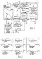
- Figure 1 is a block schematic diagram of a circuit embodying the present invention; and
- Figure 2 is a representation of the waveforms in the circuit of Figure 1.
- The circuit shown in Figure 1 consists of a digital phase-locked loop using a binary overflowing accumulator as a numerically controlled oscillator. The circuit provides elimination of frequency-dependent phase offset problems without requiring any second-order filtering, this being achieved by incorporating external compensation.
- Thus, assuming that numerically controlled
oscillator adder 1 initially contains a binary signal with all digits "0", the application of the central frequency control word, G, from the centralfrequency control unit 2, viafrequency offset adder 3 with no signal at its other input, produces a sum output which is also G. The output, A, from NCO latch 4 remains zero until the next clock pulse fromreference oscillator 5 latches the sum. At this stage, the latch output then changes to a value of G and is fed back toNCO adder 1 to produce a new output with value 2G. This is latched on the next clock pulse to produce a new latch output of value 2G. This again is fed back toadder 1 to be added to input word G. The latch output therefore increases linearly in steps of value G until the contents of theadder 1 exceed the maximum (i.e. all "1") whereupon adder 1 resets to a remainder value close to zero and the cycle begins again. The cycle duration is therefore determined by input word G; halfway through the cycle the most significant bit of the latch changes from "0" to "1", and at the end of the cycle from "1" to "0". By detecting the most-significant bit, a square wave is produced atstandard output 6 having equal mark and space with a frequency determined by B. Multiplier 7 which is controlled by loopbandwidth control unit 8 operates to adjust the loop gain and bandwidth, this multiplication preferably being implemented as a shift. - A
phase detector latch 9 samples the output value of multiplier 7 in response to a transition in the input square wave after output bysignal source 10 and passage through limiter 11. If the two signals are not in phase, the number latched is non-zero and the output oflatch 9, D, indicates the magnitude and sign of the correction needed to correct the phase error. To achieve this correction, the value of B is changed byprocessing unit 12, to produce a signal E to generate negative feedback, and applying signal E tofrequency offset adder 3.Frequency offset adder 3 allows the centre frequency of the operation of the phase locked loop to be adjusted at will. - The circuit described above is a type of first order PLL. A well know property of such systems is that there is a steady state phase error which varies as a function of the frequency difference between the input signal (F) and the centre frequency of the PLL. In order to substantially eliminate this steady state phase error, additional phase correction is provided by
comparator 13, which compares the input and the output of thephase detector latch 9 and accurately tracks the positive-going transitions of the input waveform. Supposing the input oflatch 9 is increasing from zero to the maximum "N" and the input fromsource 10 occurs when the input is M, the latch output is then also M; but since the input continues to increase, the input is greater than the output and the phase-correction output 14 remains high until the input exceeds N and becomes zero. Since the latch still contains M, the input is now less than the output and the output goes low and remains low until the input exceeds M, or whatever new number has been latched. The phase-correctedoutput 14 has the same frequency as thestandard output 6, but its transitions are synchronised to those of the reference square wave. - The phase detector based on latching the output of the numerically controlled oscillator can resolve arbitrarily small phase angles, and can produce an output which is linearly proportional to the phase error over a range of 360°.
- Figure 2 provides comparisons of the standard and phase-compensated outputs for three input frequencies. As shown by the broken lines, transitions of the phase-corrected outputs track the input phase accurately, as distinct from the tracking achieved by the standard outputs.
- The present invention is particularly suited for use in FSK modulation and demodulation e.g. in systems for signalling on electrical mains wiring. The present invention is also applicable to digital television receivers e.g. for locking with zero phase error to the line frequency or colour sub carrier.
Claims (3)
Applications Claiming Priority (2)
| Application Number | Priority Date | Filing Date | Title |
|---|---|---|---|
| GB878701573A GB8701573D0 (en) | 1987-01-24 | 1987-01-24 | Phase-locked loops |
| GB8701573 | 1987-01-24 |
Publications (3)
| Publication Number | Publication Date |
|---|---|
| EP0277726A2 true EP0277726A2 (en) | 1988-08-10 |
| EP0277726A3 EP0277726A3 (en) | 1990-02-07 |
| EP0277726B1 EP0277726B1 (en) | 1993-10-27 |
Family
ID=10611173
Family Applications (1)
| Application Number | Title | Priority Date | Filing Date |
|---|---|---|---|
| EP88300441A Expired - Lifetime EP0277726B1 (en) | 1987-01-24 | 1988-01-20 | Phase-locked loops |
Country Status (5)
| Country | Link |
|---|---|
| US (1) | US4791378A (en) |
| EP (1) | EP0277726B1 (en) |
| JP (1) | JPS63200618A (en) |
| DE (1) | DE3885116T2 (en) |
| GB (1) | GB8701573D0 (en) |
Cited By (6)
| Publication number | Priority date | Publication date | Assignee | Title |
|---|---|---|---|---|
| EP0527432A2 (en) * | 1991-08-12 | 1993-02-17 | Motorola, Inc. | A circuit and method for phase error correction in a digital receiver |
| EP0535945A2 (en) * | 1991-09-30 | 1993-04-07 | Kabushiki Kaisha Toshiba | Digital oscillator and color subcarrier demodulation circuit |
| EP0619653A1 (en) * | 1993-04-05 | 1994-10-12 | Koninklijke Philips Electronics N.V. | Digital phase-locked loop |
| EP0661815A1 (en) * | 1993-12-28 | 1995-07-05 | Mitsubishi Denki Kabushiki Kaisha | Frequency Synthesizer |
| EP0778675A1 (en) * | 1995-12-06 | 1997-06-11 | Yamaha Corporation | Digital PLL circuit |
| WO1999000901A1 (en) * | 1997-06-28 | 1999-01-07 | Robert Bosch Gmbh | Method and circuit for synchronizing a clock pulse with events occurring in a time slot system |
Families Citing this family (12)
| Publication number | Priority date | Publication date | Assignee | Title |
|---|---|---|---|---|
| US4855683A (en) * | 1987-11-18 | 1989-08-08 | Bell Communications Research, Inc. | Digital phase locked loop with bounded jitter |
| US5390207A (en) * | 1990-11-28 | 1995-02-14 | Novatel Communications Ltd. | Pseudorandom noise ranging receiver which compensates for multipath distortion by dynamically adjusting the time delay spacing between early and late correlators |
| US5101416A (en) * | 1990-11-28 | 1992-03-31 | Novatel Comunications Ltd. | Multi-channel digital receiver for global positioning system |
| US5402450A (en) * | 1992-01-22 | 1995-03-28 | Trimble Navigation | Signal timing synchronizer |
| US5414729A (en) * | 1992-01-24 | 1995-05-09 | Novatel Communications Ltd. | Pseudorandom noise ranging receiver which compensates for multipath distortion by making use of multiple correlator time delay spacing |
| JP3245925B2 (en) * | 1992-02-19 | 2002-01-15 | ソニー株式会社 | Digital PLL circuit |
| US5479457A (en) * | 1993-08-27 | 1995-12-26 | Vlsi Technology Inc. | Method and apparatus for attenuating jitter in a digital transmission line |
| US5742191A (en) * | 1993-12-08 | 1998-04-21 | Thomson Consumer Electronics, Inc. | D/A for controlling an oscillator in a phase locked loop |
| US7124153B2 (en) | 2002-03-18 | 2006-10-17 | Genesis Microchip Inc. | Frequency converter and methods of use thereof |
| US7205798B1 (en) * | 2004-05-28 | 2007-04-17 | Intersil Americas Inc. | Phase error correction circuit for a high speed frequency synthesizer |
| US7135933B2 (en) * | 2004-09-29 | 2006-11-14 | Intelliserv, Inc. | System for adjusting frequency of electrical output pulses derived from an oscillator |
| CN111030687B (en) * | 2019-12-31 | 2023-07-18 | 南华大学 | All-digital phase-locked loop based on fast full adder and phase-locked control method |
Citations (3)
| Publication number | Priority date | Publication date | Assignee | Title |
|---|---|---|---|---|
| DE2854039A1 (en) * | 1978-12-12 | 1980-07-03 | Hertz Inst Heinrich | Phase locked loop set=up - synchronises reference signal to input signal by using amplitude samples of reference signal as measure of phase |
| US4577163A (en) * | 1984-07-09 | 1986-03-18 | Honeywell Inc. | Digital phase locked loop |
| EP0177076A1 (en) * | 1984-09-03 | 1986-04-09 | Philips Patentverwaltung GmbH | Circuit for converting an analog television signal into digitized colour signals |
-
1987
- 1987-01-24 GB GB878701573A patent/GB8701573D0/en active Pending
-
1988
- 1988-01-20 DE DE88300441T patent/DE3885116T2/en not_active Expired - Fee Related
- 1988-01-20 EP EP88300441A patent/EP0277726B1/en not_active Expired - Lifetime
- 1988-01-21 US US07/146,426 patent/US4791378A/en not_active Expired - Fee Related
- 1988-01-25 JP JP63012760A patent/JPS63200618A/en active Pending
Patent Citations (3)
| Publication number | Priority date | Publication date | Assignee | Title |
|---|---|---|---|---|
| DE2854039A1 (en) * | 1978-12-12 | 1980-07-03 | Hertz Inst Heinrich | Phase locked loop set=up - synchronises reference signal to input signal by using amplitude samples of reference signal as measure of phase |
| US4577163A (en) * | 1984-07-09 | 1986-03-18 | Honeywell Inc. | Digital phase locked loop |
| EP0177076A1 (en) * | 1984-09-03 | 1986-04-09 | Philips Patentverwaltung GmbH | Circuit for converting an analog television signal into digitized colour signals |
Cited By (10)
| Publication number | Priority date | Publication date | Assignee | Title |
|---|---|---|---|---|
| EP0527432A2 (en) * | 1991-08-12 | 1993-02-17 | Motorola, Inc. | A circuit and method for phase error correction in a digital receiver |
| EP0527432A3 (en) * | 1991-08-12 | 1994-04-06 | Motorola Inc | |
| EP0535945A2 (en) * | 1991-09-30 | 1993-04-07 | Kabushiki Kaisha Toshiba | Digital oscillator and color subcarrier demodulation circuit |
| EP0535945A3 (en) * | 1991-09-30 | 1993-11-18 | Toshiba Kk | Digital oscillator and color subcarrier demodulation circuit |
| EP0619653A1 (en) * | 1993-04-05 | 1994-10-12 | Koninklijke Philips Electronics N.V. | Digital phase-locked loop |
| EP0661815A1 (en) * | 1993-12-28 | 1995-07-05 | Mitsubishi Denki Kabushiki Kaisha | Frequency Synthesizer |
| US5539346A (en) * | 1993-12-28 | 1996-07-23 | Mitsubishi Denki Kabushiki Kaisha | Frequency synthesizer having DDS in place of VCO |
| EP0778675A1 (en) * | 1995-12-06 | 1997-06-11 | Yamaha Corporation | Digital PLL circuit |
| US6005427A (en) * | 1995-12-06 | 1999-12-21 | Yamaha Corporation | Digital PLL circuit |
| WO1999000901A1 (en) * | 1997-06-28 | 1999-01-07 | Robert Bosch Gmbh | Method and circuit for synchronizing a clock pulse with events occurring in a time slot system |
Also Published As
| Publication number | Publication date |
|---|---|
| DE3885116T2 (en) | 1994-04-28 |
| EP0277726B1 (en) | 1993-10-27 |
| DE3885116D1 (en) | 1993-12-02 |
| EP0277726A3 (en) | 1990-02-07 |
| GB8701573D0 (en) | 1987-02-25 |
| JPS63200618A (en) | 1988-08-18 |
| US4791378A (en) | 1988-12-13 |
Similar Documents
| Publication | Publication Date | Title |
|---|---|---|
| US4791378A (en) | Phase-locked loops | |
| EP0342736B1 (en) | Phase-locked-loop cicuit and bit-detection arrangement comprising such a phase-locked-loop circuit | |
| US5130671A (en) | Phase-locked loop frequency tracking device including a direct digital synthesizer | |
| EP1057252B1 (en) | Direct digital synthesis of precise, stable angle modulated rf signal | |
| CA2130269C (en) | Psk demodulator | |
| US4015083A (en) | Timing recovery circuit for digital data | |
| US4806878A (en) | Phase comparator lock detect circuit and a synthesizer using same | |
| US4520319A (en) | Electronic phase detector having an output which is proportional to the phase difference between two data signals | |
| US8036614B2 (en) | Replica DLL for phase resetting | |
| US5258724A (en) | Frequency synthesizer | |
| US5184092A (en) | Phase-locked loop frequency tracking device including a direct digital synthesizer | |
| US4495473A (en) | Digital phase shifting apparatus which compensates for change of frequency of an input signal to be phase shifted | |
| US5062123A (en) | Kalman predictor for providing a relatively noise free indication of the phase of a carrier laden with noise | |
| JPH0795685B2 (en) | Programmable high-speed digital phase-locked loop | |
| US4333060A (en) | Phase locked loop for recovering data bit timing | |
| EP0527034A2 (en) | Digital phase-locked loop circuit | |
| Hurd et al. | Digital transition tracking symbol synchronizer for low SNR coded systems | |
| US4849704A (en) | Duty cycle independent phase detector | |
| US5859551A (en) | Digital PLL circuit | |
| US6255858B1 (en) | Phase-frequency detector and phase-locked loop circuit incorporating the same | |
| EP0778675B1 (en) | Digital PLL circuit | |
| US4635103A (en) | Phase locked loop system incorporating automatic gain control | |
| EP0259867A2 (en) | Demodulator for psk-modulated signals | |
| US4184122A (en) | Digital phase comparison apparatus | |
| US6577695B1 (en) | Emulating narrow band phase-locked loop behavior on a wide band phase-locked loop |
Legal Events
| Date | Code | Title | Description |
|---|---|---|---|
| PUAI | Public reference made under article 153(3) epc to a published international application that has entered the european phase |
Free format text: ORIGINAL CODE: 0009012 |
|
| AK | Designated contracting states |
Kind code of ref document: A2 Designated state(s): DE FR GB IT NL |
|
| PUAL | Search report despatched |
Free format text: ORIGINAL CODE: 0009013 |
|
| AK | Designated contracting states |
Kind code of ref document: A3 Designated state(s): DE FR GB IT NL |
|
| 17P | Request for examination filed |
Effective date: 19900312 |
|
| 17Q | First examination report despatched |
Effective date: 19920508 |
|
| GRAA | (expected) grant |
Free format text: ORIGINAL CODE: 0009210 |
|
| AK | Designated contracting states |
Kind code of ref document: B1 Designated state(s): DE FR GB IT NL |
|
| PG25 | Lapsed in a contracting state [announced via postgrant information from national office to epo] |
Ref country code: IT Free format text: LAPSE BECAUSE OF FAILURE TO SUBMIT A TRANSLATION OF THE DESCRIPTION OR TO PAY THE FEE WITHIN THE PRE;WARNING: LAPSES OF ITALIAN PATENTS WITH EFFECTIVE DATE BEFORE 2007 MAY HAVE OCCURRED AT ANY TIME BEFORE 2007. THE CORRECT EFFECTIVE DATE MAY BE DIFFERENT FROM THE ONE RECORDED.SCRIBED TIME-LIMIT Effective date: 19931027 Ref country code: NL Effective date: 19931027 |
|
| REF | Corresponds to: |
Ref document number: 3885116 Country of ref document: DE Date of ref document: 19931202 |
|
| ET | Fr: translation filed | ||
| PG25 | Lapsed in a contracting state [announced via postgrant information from national office to epo] |
Ref country code: GB Effective date: 19940127 |
|
| NLV1 | Nl: lapsed or annulled due to failure to fulfill the requirements of art. 29p and 29m of the patents act | ||
| PLBE | No opposition filed within time limit |
Free format text: ORIGINAL CODE: 0009261 |
|
| STAA | Information on the status of an ep patent application or granted ep patent |
Free format text: STATUS: NO OPPOSITION FILED WITHIN TIME LIMIT |
|
| GBPC | Gb: european patent ceased through non-payment of renewal fee |
Effective date: 19940127 |
|
| PG25 | Lapsed in a contracting state [announced via postgrant information from national office to epo] |
Ref country code: FR Effective date: 19940930 |
|
| PG25 | Lapsed in a contracting state [announced via postgrant information from national office to epo] |
Ref country code: DE Effective date: 19941001 |
|
| 26N | No opposition filed | ||
| REG | Reference to a national code |
Ref country code: FR Ref legal event code: ST |