EP0276090A1 - Kollektor für geladene Partikel - Google Patents
Kollektor für geladene Partikel Download PDFInfo
- Publication number
- EP0276090A1 EP0276090A1 EP88300302A EP88300302A EP0276090A1 EP 0276090 A1 EP0276090 A1 EP 0276090A1 EP 88300302 A EP88300302 A EP 88300302A EP 88300302 A EP88300302 A EP 88300302A EP 0276090 A1 EP0276090 A1 EP 0276090A1
- Authority
- EP
- European Patent Office
- Prior art keywords
- electrodes
- electrode
- collector
- charged
- cathode
- Prior art date
- Legal status (The legal status is an assumption and is not a legal conclusion. Google has not performed a legal analysis and makes no representation as to the accuracy of the status listed.)
- Granted
Links
Images


Classifications
-
- H—ELECTRICITY
- H01—ELECTRIC ELEMENTS
- H01J—ELECTRIC DISCHARGE TUBES OR DISCHARGE LAMPS
- H01J23/00—Details of transit-time tubes of the types covered by group H01J25/00
- H01J23/02—Electrodes; Magnetic control means; Screens
- H01J23/027—Collectors
- H01J23/0275—Multistage collectors
Definitions
- the present invention relates to a charged-particle collector and, more particularly, to a multistage depressed electron collector
- a traveling stream of charged-particles such as electrons
- a microwave traveling wave tube incorporates a source of electrons that are formed into a beam, in which the electrons are accelerated to a predetermined velocity and directed along an axial path through an "interaction" region within the microwave tube body.
- interaction region kinetic energy is transferred from the moving electrons to the high frequency electromagnetic fields, such as microwave signals, that are propagating along a slow wave structure through the interaction region at about the same velocity as the moving electrons.
- the electrons give up energy to the microwave field through the exchange process characterized as electronic interaction, evidenced by a lower velocity of the electrons exiting from the interaction region.
- the "spent" electrons pass out of the interaction region where they are incident upon and collected by a final tube element, termed the collector.
- the collector collects and returns the incident electrons to the voltage source.
- much of the energy in a moving particle is released in the form of heat when the particle strikes a stationary element, such as the collector. This produces undesired heating in the microwave tube and a lower overall electrical efficiency of microwave tube operation.
- the depressed collector and, more particularly, the multistage depressed collector is a collector that increases the electrical efficiency of traveling wave tube operation as well as reduces undesirable heat generation by a process of velocity sorting of the electrons controlled by a retarding electric field.
- the field slows the electrons so that the electrons are collected by electrodes at a reduced velocity and ideally at a zero velocity.
- the multistage depressed collector is characterized physically by a series of spaced metal electrodes, each containing a passage therethrough, a final electrode and a passage entry for receiving electrons.
- the electrodes are maintained at successively lower voltages with respect to the tube circuit taken as ground (or at successivelysively higher negative voltages as otherwise viewed) so as to present a retarding electric field to the electrons which pass through the entrance into the collector region.
- Such types of devices are substantially well developed and hence are complex in nature as is known to the reader skilled in the art.
- One type of known multistage depressed collector employs a combination of a transverse electric field and a longitudinal magnetic field for sorting electrons as a function of electron velocity. See U.S. Letters Patent No. 3,526,805, by Okashi, et al.; No. 3,644,778, by Mihran, et al.; and No. 3,702,951, by Kosmahl.
- Another type of collector employs a retarding electric field established by a cuplike electrode and a pointed spike located in the center of the cuplike member. The effect of this structure with a voltage applied is to present an electron mirror with a negative focal length to electrons moving near the axis. Hence, the reflected beam is more divergent than the incident beam. See the paper entitled Multistage Depressed Collector Investigation For Travelling Way Tubes , Tammaru, NASA CR-72950 EDDW-3207, Contract NAS-3-11536, Final Contract Report.
- NASA collector The efficiency of the NASA collector is limited by the defocusing properties of the spikelike reflector. Further, the collectors shown in the patents mentioned above required the maintenance of an axial magnetic field of a critical magnitude for proper functioning.
- a charged-particle collector for collecting charged particles comprising: an enclosed region having a longitudinal axis passing through the center of said enclosed region into which the charged particles are directed; and a plurality of electrodes for collecting the charged particles, each of said electrodes being arranged about said longitudinal axis and having a surface area which is substantially symmetrical about said longitudinal axis, at least one of said electrodes also containing an aperture through which the charged particles are directed, said aperture being offset from said longitudinal axis.
- a preferred embodiment is formed from a series of electrodes, a first of which forms an electron entry wall, while a final electrode forms a back wall fo the electron collection sealed by appropriate side walls between the first and final electrodes.
- Located between the first and final electrodes may be one or more further electrodes which, along with the first and final electrode, are symmetrical about a common axis forming the longitudinal axis of the electron collector.
- the first or entry electrode has an electron receiving aperture therein that is offset from the longitudinal axis of the axisymmetrical electrode.
- additional electrodes may be provided with apertures which may or may not be offset to form a passageway for the electrons that is offset or off-axis from the longitudinal axis of the electron collector.
- the axisymmetrical electrodes form an axisymmetrical electrostatic field when the electrodes are connected to a voltage potential. This field serves to focus the electrons entering the collector upon the various electrodes depending upon the energy level of each electron.
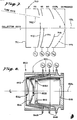
- Fig. 1 shows a charged-particle collector 10 which may be used to collect electrons having a plurality of electrodes 12, 14, 16, and 18 formed from a metal such as copper, into a generally cuplike shape with each electrode nested into the other. While four electrodes are shown, as few as two and more than four electrodes may be used within the present invention.
- the left-most electrode 12 forms a particle entry wall of the collector 10, while the right-most electrode 18 forms the furthest electrode or back wall of the collector 10.
- the side walls of collector 10 are formed by ceramic cylinders 20 which mechanically separate and electrically isolate one electrode from the other.
- electrodes 12 and 18 may be the only two electrodes required for the collector 10.
- Mounted at a slight distance from electrode 12 is a mounting plate 22 which may be fabricated from an insulating material.
- Electrodes 12, 14, and 16 are each provided with apertures; 26, 28 and 30, respectively, through which an electron beam 32 generated from a cathode 34 passes. It will be noted that apertures 26, 28 and, in some cases, 30 are offset from the axis 24 of the electron collector 10 for providing an off-axis injection of electron beam 32.
- the electron beam 32 is generated by an electron gun 36 which may comprise a cathode 34, control grids 38, and an anode 39.
- a vacuum device 40 such as a microwave device or, more particularly, a traveling wave tube.
- the spent electrons exit the microwave device 40 where they may be refocused by a magnetic field formed by permanent magnet 42 and/or an exit anode 44.
- the exit anode 44 may be mounted in close proximity to the left-most electrode 12 and is provided with an aperture therein which is in alignment with the offset aperture 26 of electrode 12.
- the precise configuration of the electrodes 12-18 within the electron collector 10 may vary as well as the number of such electrodes.
- the important feature of the electrodes 12-18 is that they focus the electron beam. Focus means a selective focus wherein different electrons which make up the beam 32 are selected by energy level for shunting within a generally circular area upon different and separate electrodes.
- Focus means a selective focus wherein different electrons which make up the beam 32 are selected by energy level for shunting within a generally circular area upon different and separate electrodes.
- an infinite number of electrodes provide a target for an infinite number of electron energy levels so that each electron strikes an appropriate electrode with a zero velocity. In practice, the infinite number of electrodes is reduced to meet the need for a simplified design.
- V 2/3z + 1/2z2 - 1/12z4 - 1/4 r2 + 1/4r2z2 - 1/32r4 where the electrostatic potential, V, is described in an r, z-coordinate system.
- R is the radius from the longitudinal axis 24 of the collector 10, while z is the length along that axis.
- any equal potential surface can be substituted by a conducting electrode at the proper potential.
- the configuration of the focusing electrodes follows to some extent the contours shown in Fig. 3.
- a computer to project the various trajectories of an off-axis electron beam 32 as it enters the electron collector 10, it is possible to plot curves similar to that shown in Fig. 4 wherein a plot representing the projections of the electron trajectories on the y, z-plane is shown.
- Fig. 4 shows an electron beam 32 entering parallel to the longitudinal axis 24 of the collector 10 and assumes that all electrons within the beam have the same energy level which is 92% of the cathode voltage.
- FIG. 5 shows the intensity of beam 32 as it passes into the electron collector 10 at a point where the potential of the electrostatic field is approximately 40% of the cathode.
- Fig. 6 shows the pattern of the beam 32 at a point where the beam has a potential of 25% with respect to the cathode.
- the beam 32 includes two trajectory areas including a first area shown in the upper surface where the beam 32 is moving from left to right (Fig. 4) and a second portion wherein the beam 32 ⁇ is moving from right to left.
- the return beam 32 ⁇ is shown by squares which represent theoretical strike points of the spent electrons.
- electrons entering the electron collector 10 are focused in a generally circular area upon the rear or inner surfaces of the electrodes 12-16 depending upon the energy level of each electron.
- a schematic design of a suitable electron collector 710 is shown having a plurality of electrodes 711, 712, 714, 718, and 719. Note, how the configuration of the electrode 712, 714, 718, and 719 comply with the equipotential lines shown in Fig. 3.
- the potential applied to electrode 712 is 55% of the cathode voltage from ground or plus 45% when compared to the cathode voltage.
- the voltage on electrode 714 is plus 35% the voltage on electrode 718 is plus 10% and the voltage on electrode 719 is 0 with respect to the cathode. That is, the grid 719 is 100% depressed.
- the electron beam 732 is offset from axis 724 and is shown entering electron collector 710 at an angle to the collector axis 724 of approximatley 10°, although other angles between 6° and 14° may be used.
- the zero voltage grid 719 is unnecessary within the present invention. That is, the electrode 719 which is 100% depressed has a tendency to turn the electrons aound and send them back through the opening within the electron collector 710. Thus, it was unexpectedly found that the elimination of the 100% depressed electrode 719 not only retained the efficiency of the electron collector 710 but, in fact, improved it. Further, by experimentation, it was found that the efficiency of the electron collector remained the same whether the electron beam 732 entered the collector 710 at an angle, as shown in Fig. 7, or entered the collector parallel to its axis 724. This unexpected result was extremely useful as it simplifies the design of the collector. This simplified design makes it possible to fabricate all electrodes axisymmetrically about the centerline 724. The only feature of the electrodes that is not axisymmetrical is the offset apertures for the electron beam 732.
- the electron collector 810 shown in Fig. 8 includes four electrodes 812, 814, 816, and 818. These cuplike metal electrodes are provided with outwardly extending flanges 848 which are mechanically and electrically separated from each other by insulators 820.
- the insulators 820 may be attached to flanges 848 by any suitable device such as by chemical bonding or electrical welding.
- electrodes 812, 814, 816, and 818 are symmetrical about a centerline 824 but for the apertures 826 and 828 in the left-most electrodes.
- Aperture 826 in electrode 812 is offset from the centerline 824 by a significant distance; while aperture 828 in electrode 814 is offset by a slightly smaller distance, although the aperture 828 is significantly larger.
- the aperture 830 in electrode 816 is shown as symmetrical even though it is utilized to capture an electron beam, such as beam 32 in Fig. 1 which is entering off-axis to the centerline 824 of the collector 810.
- the offset apertures 826 and 828 are circular in shape within the preferred embodiments. However, other shapes such as elliptical or oval may also be used.
- the left-most surface of electrode 812 is shown flat, while the inner surface thereof is made thicker toward the centerline 824 for purposes of focusing the electron beam. Similarly, the left-most surface of electrode 814 is dished; while the inner surface thereof is arranged in a parallel configuration thereto. This aids in focusing the beam 32 (Fig. 1).
- the aperture 828 passes through the flat portion of the dish in electrode 814 as well as part of the tappering surface thereof.
- Aperture 830 in electrode 816 is symmetrical, as stated above.
- the electrode 818 which forms the final electrode or rear wall of collector 810 is maintained at the same potential as electrode 816. As stated above, it was unexpectedly discovered that it is not desirable to depress the final electrode to a potential equal to the cathode. Rather, a potential slightly positive compared to the cathode is desirable for improved efficiency.
- the first electrode 812 was retained at 58% of the cathode voltage from ground
- the second electrode 814 was retained at 80% of the cathode voltage from ground
- the third electrode 816 was maintained at 90% of the cathode voltage from ground along with electrode 818.
- the range of voltage on electrode 812 may vary from 30 to 65% of the cathode voltage from ground
- the voltage on electrode 814 may vary from 55 to 85%
- the voltage on electrodes 816 and 818 may vary from 80 to 100%.
- Fig. 9 shows the electrodes of Fig. 8 in an exploded view to more clearly demonstrate the relationship of the off-axis beam injection through the offset apertures and the simplified fabrication of the axisymmetrical electrodes.
- Electrode 812 could be dished like electrode 814 in some application. It will be understood that the heat caused by the electron beam 32 as it strikes the electrodes may be dissipated by liquid cooling or by fins or other suitable arrangements.
- the electron gun 36 and the vacuum device 40 which are utilized with the electron collector 10 of the present invention should not be limited by the devices shown schematically herein. Accordingly, the present invention should be limited only by the appended claims.
Landscapes
- Microwave Tubes (AREA)
Applications Claiming Priority (2)
| Application Number | Priority Date | Filing Date | Title |
|---|---|---|---|
| US07/006,010 US4794303A (en) | 1987-01-22 | 1987-01-22 | Axisymmetric electron collector with off-axis beam injection |
| US6010 | 2007-12-14 |
Publications (2)
| Publication Number | Publication Date |
|---|---|
| EP0276090A1 true EP0276090A1 (de) | 1988-07-27 |
| EP0276090B1 EP0276090B1 (de) | 1992-12-30 |
Family
ID=21718837
Family Applications (1)
| Application Number | Title | Priority Date | Filing Date |
|---|---|---|---|
| EP88300302A Expired EP0276090B1 (de) | 1987-01-22 | 1988-01-14 | Kollektor für geladene Partikel |
Country Status (3)
| Country | Link |
|---|---|
| US (1) | US4794303A (de) |
| EP (1) | EP0276090B1 (de) |
| DE (1) | DE3877004T2 (de) |
Cited By (2)
| Publication number | Priority date | Publication date | Assignee | Title |
|---|---|---|---|---|
| DE4033101A1 (de) * | 1990-10-18 | 1992-04-23 | Licentia Gmbh | Elektronenkollektor fuer eine hochfrequenz-elektronenstrahlroehre |
| EP1322035A2 (de) * | 2001-12-14 | 2003-06-25 | NEC Microwave Tube, Ltd. | Wanderfeldröhre |
Families Citing this family (16)
| Publication number | Priority date | Publication date | Assignee | Title |
|---|---|---|---|---|
| US5389854A (en) * | 1992-07-21 | 1995-02-14 | Litton Systems, Inc. | Collector ion expeller |
| US5436525A (en) * | 1992-12-03 | 1995-07-25 | Litton Systems, Inc. | Highly depressed, high thermal capacity, conduction cooled collector |
| US5420478A (en) * | 1993-02-12 | 1995-05-30 | Litton Systems, Inc. | Depressed collector for sorting radial energy level of a gyrating electron beam |
| GB2281656B (en) * | 1993-09-03 | 1997-04-02 | Litton Systems Inc | Radio frequency power amplification |
| US6380803B2 (en) | 1993-09-03 | 2002-04-30 | Litton Systems, Inc. | Linear amplifier having discrete resonant circuit elements and providing near-constant efficiency across a wide range of output power |
| US5780970A (en) * | 1996-10-28 | 1998-07-14 | University Of Maryland | Multi-stage depressed collector for small orbit gyrotrons |
| US5952785A (en) * | 1997-07-17 | 1999-09-14 | Komm; David S. | Transverse field collector for a traveling wave tube |
| US6617791B2 (en) | 2001-05-31 | 2003-09-09 | L-3 Communications Corporation | Inductive output tube with multi-staged depressed collector having improved efficiency |
| US20040222744A1 (en) * | 2002-11-21 | 2004-11-11 | Communications & Power Industries, Inc., | Vacuum tube electrode structure |
| GB2411517A (en) * | 2004-02-27 | 2005-08-31 | E2V Tech Uk Ltd | Collector arrangement |
| US7368874B2 (en) * | 2005-02-18 | 2008-05-06 | Communications and Power Industries, Inc., Satcom Division | Dynamic depressed collector |
| US20110121194A1 (en) * | 2006-10-16 | 2011-05-26 | Bhatt Ronak J | Controlled transport system for an elliptic charged-particle beam |
| DE102012100132A1 (de) | 2012-01-10 | 2013-07-11 | Thales Air Systems & Electron Devices Gmbh | Auffänger für eine Wanderfeldröhre und Wanderfeldröhre mit einem solchen Auffänger |
| US8813295B1 (en) | 2013-05-02 | 2014-08-26 | Clarence E. Washington | Ticket scratching device |
| CN104157536B (zh) * | 2014-08-21 | 2016-04-27 | 中国科学院电子学研究所 | 非轴对称双斜面的多级降压收集极电极 |
| CN105762048B (zh) * | 2016-04-06 | 2018-03-02 | 中国电子科技集团公司第十二研究所 | 内收集极和包括该内收集极的收集极及行波管 |
Citations (1)
| Publication number | Priority date | Publication date | Assignee | Title |
|---|---|---|---|---|
| GB1549923A (en) * | 1976-10-04 | 1979-08-08 | Litton Systems Inc | Multistage depressed collector |
Family Cites Families (7)
| Publication number | Priority date | Publication date | Assignee | Title |
|---|---|---|---|---|
| US3368104A (en) * | 1964-03-17 | 1968-02-06 | Varian Associates | Electron beam tube included depressed collector therefor |
| US3644778A (en) * | 1969-10-23 | 1972-02-22 | Gen Electric | Reflex depressed collector |
| US3764850A (en) * | 1972-06-27 | 1973-10-09 | Nasa | Electron beam controller |
| US3936695A (en) * | 1974-04-26 | 1976-02-03 | Varian Associates | Electron collector having means for trapping secondary electrons in a linear beam microwave tube |
| DE2744228A1 (de) * | 1977-09-30 | 1979-04-05 | Siemens Ag | Mehrstufen-kollektor fuer laufzeitroehren |
| FR2480497A1 (fr) * | 1980-04-15 | 1981-10-16 | Thomson Csf | Collecteur deprime a plusieurs etages pour tube hyperfrequence et tube hyperfrequence comportant un tel collecteur |
| US4527092A (en) * | 1983-09-30 | 1985-07-02 | The United States Of America As Represented By The Administrator Of The National Aeronautics And Space Administration | Multistage spent particle collector and a method for making same |
-
1987
- 1987-01-22 US US07/006,010 patent/US4794303A/en not_active Expired - Lifetime
-
1988
- 1988-01-14 DE DE8888300302T patent/DE3877004T2/de not_active Expired - Lifetime
- 1988-01-14 EP EP88300302A patent/EP0276090B1/de not_active Expired
Patent Citations (1)
| Publication number | Priority date | Publication date | Assignee | Title |
|---|---|---|---|---|
| GB1549923A (en) * | 1976-10-04 | 1979-08-08 | Litton Systems Inc | Multistage depressed collector |
Cited By (3)
| Publication number | Priority date | Publication date | Assignee | Title |
|---|---|---|---|---|
| DE4033101A1 (de) * | 1990-10-18 | 1992-04-23 | Licentia Gmbh | Elektronenkollektor fuer eine hochfrequenz-elektronenstrahlroehre |
| EP1322035A2 (de) * | 2001-12-14 | 2003-06-25 | NEC Microwave Tube, Ltd. | Wanderfeldröhre |
| EP1322035A3 (de) * | 2001-12-14 | 2004-08-11 | NEC Microwave Tube, Ltd. | Wanderfeldröhre |
Also Published As
| Publication number | Publication date |
|---|---|
| DE3877004T2 (de) | 1993-06-17 |
| US4794303A (en) | 1988-12-27 |
| DE3877004D1 (de) | 1993-02-11 |
| EP0276090B1 (de) | 1992-12-30 |
Similar Documents
| Publication | Publication Date | Title |
|---|---|---|
| EP0276090B1 (de) | Kollektor für geladene Partikel | |
| EP0934599B1 (de) | Vorgespannter mehrstuffenkollektor für kleinumlaufbahngyrotrons | |
| JPH0360139B2 (de) | ||
| US4096409A (en) | Multistage depressed collector | |
| US2853641A (en) | Electron beam and wave energy interaction device | |
| EP0097535A2 (de) | Geschwindigkeitsfilter mit gekreuzten Feldern und Ionenstrahlbehandlungssystem | |
| US4287419A (en) | Strong focus space charge | |
| EP1266390A1 (de) | Gerillter mehrstuffenkollektor zur unterdrückung von sekundärelektronen | |
| US4439395A (en) | Neutral beamline with improved ion energy recovery | |
| US4398122A (en) | Multistage depressed collector for microwave tube | |
| EP0475199A2 (de) | Quelle zur Erzeugung eines schnellen Atomstrahls | |
| US3188515A (en) | Beam collector with auxiliary collector for repelled or secondarily-emitted electrons | |
| US4349505A (en) | Neutral beamline with ion energy recovery based on magnetic blocking of electrons | |
| US5283534A (en) | High frequency amplifying apparatus with a collector which has a periodic amplitude variable longitudinal magnetic field therein | |
| US6974950B2 (en) | Positive and negative ion beam merging system for neutral beam production | |
| US4401918A (en) | Klystron having electrostatic quadrupole focusing arrangement | |
| EP0975002B1 (de) | Kollektor mit transversalem Feld | |
| Mobley et al. | Gabor lenses | |
| US3551728A (en) | High intensity linear accelerators | |
| US3649862A (en) | Separated ion beam source with adjustable separation | |
| US5389854A (en) | Collector ion expeller | |
| US4085376A (en) | Device for electrical deceleration of flow of charged particles | |
| US4329586A (en) | Electron energy recovery system for negative ion sources | |
| RU2291514C1 (ru) | Многоэлектродный коллектор электровакуумного свч-прибора о-типа | |
| US5028837A (en) | Low energy ion trap |
Legal Events
| Date | Code | Title | Description |
|---|---|---|---|
| PUAI | Public reference made under article 153(3) epc to a published international application that has entered the european phase |
Free format text: ORIGINAL CODE: 0009012 |
|
| AK | Designated contracting states |
Kind code of ref document: A1 Designated state(s): DE FR GB |
|
| 17P | Request for examination filed |
Effective date: 19881117 |
|
| 17Q | First examination report despatched |
Effective date: 19900905 |
|
| GRAA | (expected) grant |
Free format text: ORIGINAL CODE: 0009210 |
|
| AK | Designated contracting states |
Kind code of ref document: B1 Designated state(s): DE FR GB |
|
| ET | Fr: translation filed | ||
| REF | Corresponds to: |
Ref document number: 3877004 Country of ref document: DE Date of ref document: 19930211 |
|
| PLBE | No opposition filed within time limit |
Free format text: ORIGINAL CODE: 0009261 |
|
| STAA | Information on the status of an ep patent application or granted ep patent |
Free format text: STATUS: NO OPPOSITION FILED WITHIN TIME LIMIT |
|
| 26N | No opposition filed | ||
| REG | Reference to a national code |
Ref country code: GB Ref legal event code: IF02 |
|
| REG | Reference to a national code |
Ref country code: GB Ref legal event code: 732E |
|
| PGFP | Annual fee paid to national office [announced via postgrant information from national office to epo] |
Ref country code: GB Payment date: 20070125 Year of fee payment: 20 |
|
| PGFP | Annual fee paid to national office [announced via postgrant information from national office to epo] |
Ref country code: DE Payment date: 20070228 Year of fee payment: 20 |
|
| REG | Reference to a national code |
Ref country code: GB Ref legal event code: PE20 |
|
| PGFP | Annual fee paid to national office [announced via postgrant information from national office to epo] |
Ref country code: FR Payment date: 20070117 Year of fee payment: 20 |
|
| PG25 | Lapsed in a contracting state [announced via postgrant information from national office to epo] |
Ref country code: GB Free format text: LAPSE BECAUSE OF EXPIRATION OF PROTECTION Effective date: 20080113 |