EP0274380A2 - Driving circuit for thin film EL display device - Google Patents
Driving circuit for thin film EL display device Download PDFInfo
- Publication number
- EP0274380A2 EP0274380A2 EP88100059A EP88100059A EP0274380A2 EP 0274380 A2 EP0274380 A2 EP 0274380A2 EP 88100059 A EP88100059 A EP 88100059A EP 88100059 A EP88100059 A EP 88100059A EP 0274380 A2 EP0274380 A2 EP 0274380A2
- Authority
- EP
- European Patent Office
- Prior art keywords
- data side
- driving circuit
- thin film
- switching
- electrodes
- Prior art date
- Legal status (The legal status is an assumption and is not a legal conclusion. Google has not performed a legal analysis and makes no representation as to the accuracy of the status listed.)
- Withdrawn
Links
Images


Classifications
-
- G—PHYSICS
- G09—EDUCATION; CRYPTOGRAPHY; DISPLAY; ADVERTISING; SEALS
- G09G—ARRANGEMENTS OR CIRCUITS FOR CONTROL OF INDICATING DEVICES USING STATIC MEANS TO PRESENT VARIABLE INFORMATION
- G09G3/00—Control arrangements or circuits, of interest only in connection with visual indicators other than cathode-ray tubes
- G09G3/20—Control arrangements or circuits, of interest only in connection with visual indicators other than cathode-ray tubes for presentation of an assembly of a number of characters, e.g. a page, by composing the assembly by combination of individual elements arranged in a matrix no fixed position being assigned to or needed to be assigned to the individual characters or partial characters
- G09G3/22—Control arrangements or circuits, of interest only in connection with visual indicators other than cathode-ray tubes for presentation of an assembly of a number of characters, e.g. a page, by composing the assembly by combination of individual elements arranged in a matrix no fixed position being assigned to or needed to be assigned to the individual characters or partial characters using controlled light sources
- G09G3/30—Control arrangements or circuits, of interest only in connection with visual indicators other than cathode-ray tubes for presentation of an assembly of a number of characters, e.g. a page, by composing the assembly by combination of individual elements arranged in a matrix no fixed position being assigned to or needed to be assigned to the individual characters or partial characters using controlled light sources using electroluminescent panels
-
- G—PHYSICS
- G09—EDUCATION; CRYPTOGRAPHY; DISPLAY; ADVERTISING; SEALS
- G09G—ARRANGEMENTS OR CIRCUITS FOR CONTROL OF INDICATING DEVICES USING STATIC MEANS TO PRESENT VARIABLE INFORMATION
- G09G2310/00—Command of the display device
- G09G2310/02—Addressing, scanning or driving the display screen or processing steps related thereto
- G09G2310/0264—Details of driving circuits
- G09G2310/0267—Details of drivers for scan electrodes, other than drivers for liquid crystal, plasma or OLED displays
-
- G—PHYSICS
- G09—EDUCATION; CRYPTOGRAPHY; DISPLAY; ADVERTISING; SEALS
- G09G—ARRANGEMENTS OR CIRCUITS FOR CONTROL OF INDICATING DEVICES USING STATIC MEANS TO PRESENT VARIABLE INFORMATION
- G09G2310/00—Command of the display device
- G09G2310/02—Addressing, scanning or driving the display screen or processing steps related thereto
- G09G2310/0264—Details of driving circuits
- G09G2310/0275—Details of drivers for data electrodes, other than drivers for liquid crystal, plasma or OLED displays, not related to handling digital grey scale data or to communication of data to the pixels by means of a current
-
- G—PHYSICS
- G09—EDUCATION; CRYPTOGRAPHY; DISPLAY; ADVERTISING; SEALS
- G09G—ARRANGEMENTS OR CIRCUITS FOR CONTROL OF INDICATING DEVICES USING STATIC MEANS TO PRESENT VARIABLE INFORMATION
- G09G2310/00—Command of the display device
- G09G2310/02—Addressing, scanning or driving the display screen or processing steps related thereto
- G09G2310/0264—Details of driving circuits
- G09G2310/0281—Arrangement of scan or data electrode driver circuits at the periphery of a panel not inherent to a split matrix structure
-
- G—PHYSICS
- G09—EDUCATION; CRYPTOGRAPHY; DISPLAY; ADVERTISING; SEALS
- G09G—ARRANGEMENTS OR CIRCUITS FOR CONTROL OF INDICATING DEVICES USING STATIC MEANS TO PRESENT VARIABLE INFORMATION
- G09G2330/00—Aspects of power supply; Aspects of display protection and defect management
- G09G2330/02—Details of power systems and of start or stop of display operation
- G09G2330/021—Power management, e.g. power saving
- G09G2330/023—Power management, e.g. power saving using energy recovery or conservation
Definitions
- This invention relates to a driving circuit for an alternating current drive type of capacitive flat matrix display panel, that is a driving circuit for a thin film EL (electroluminescence)display device.
- a double insulation type (or triple layer structure thin film EL device is composed as follows.
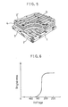
- transparent electrodes 2 which are made from In2O3, and which are formed in a band shape are provided on a glass substrate 1 in such a manner that they are disposed in parallel to each other.
- a dielectric material 3 such as Y2O3, Si3N4, Al2O3, an EL layer 4 made of ZnS in which an activator such as Mn is doped, and a dielectric material 3 ⁇ such as Y2O3, Si3N4, TiO2 or Al2O3 are respectively formed in thin films of 500 to 10000 ⁇ thickness by a thin film technology such as vapor deposition or spattering, and they are then laminated such as to form three layers.
- band-shaped back plates 5 made of Al2O3 are formed in parallel on the three layers in the direction perpendicular to the transparent electrodes 2.
- the above thin film EL device is formed in such a manner that the EL material 4 ⁇ sandwiched in between the dielectric materials 3 and 3 ⁇ is interposed between the electrodes, it can be considered as a capactive device from the view point of the circuit equivalency.
- the thin film EL device is driven by a relatively high level voltage substantially equal to 200V.
- the thin film EL device has the capacity to emit bright light due to its a.c. electric field and exhibits a long life.
- the applicant of the present invention has previously proposed a driving device comprising a scanning side driver IC as a driving circuit for scanning side electrodes.
- the scanning side driver IC comprises transistors which apply negative voltage to data side electrodes and transistors which apply positive voltage to the same.
- the driving device in order to serve as a driving circuit for the data side electrodes, the driving device comprises a data side driver IC which has transistors for charging the EL layer up to the modulation voltage, transistors for discharging the one, and diodes each connected in the inverse direction to the direction of electric current flow of the corresponding transistors.
- modulation drive may be performed on the data side with the use of the charging and discharging transistors driven by display data.
- field reverse drive is performed with the use of N-ch transistors and P-ch transistors.
- successive drive of scanning lines may be performed with the polarities of a writing waveform applied to picture elements reversed every other scanning line.
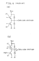
- the above mentioned driving device comprises, as shown in Fig. 4 (a), a charge side transistor UT of the data side driver IC which is made of a bipolar type of NPN transistor, no electric current is conducted from a common line Vcc to the charge side transistor UT when the charge side transistor UT is switched off.
- Fig. 4 (b) inevitable current flow cannot be prevented only in a case where the data side electrode is negative.
- the reason why the inevitable flow occurs is that although the base potential of the charge side transistor UT is arranged to be zero in the data side driver IC for the purpose of turning off it, a parasitic diode disposed between the base and the emitter is arranged to be in the forward direction when the potential of the data side electrode is negative because the transistor is the NPN type. As a result of this, the base current flows to cause the transistor UT to be turned on, thereby allowing a collector current to flow.
- the data side electrode inevitably becomes negative because the thin film EL display device needs to be driven in an alternating current manner. Therefore, if the thin film EL display device is driven by a conventional driver IC, an excessive amount of current will be lost.
- the electrical charge which has been accummulated in the thin film EL display device is fully consumed by resistance factors on the driving circuit at the time of discharge.
- an active type (self-luminescent type) of display basically consumes a large amount of electricity, it is desired to decrease the electricity consumption.
- the driving circuit comprises ; scanning side driver ICs which are formed by switching elements for applying positive voltage to the scanning side electrodes and switching elements for applying negative voltage to the same, and switching circuits for selectively applying writing voltage or 0 V to a common line of the scanning side driver ICs; a data side driver IC formed by switching elements for charging and switching elements for discharging connected to the data side electrodes, and switching circuits for applying modulation voltage connected to a pull-up common line of the data side driver ICs; and the switching circuits connected to the data side driver IC provided with switches for taking out charge stored in the thin film EL display device after the thin film EL device has emitted light and a capacitor for storing the charge taken out.
- An object of the present invention is to provide a driving circuit for a thin film EL display device in which electricity consumption at the modulation drive can be dramatically reduced by way of charging an external capacitor with a part portion of the charge in the display device and reusing the charge in the next modulation drive.
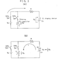
- Fig. 1 is a view illustrating the structure of a driving circuit according to an embodiment of the present invention.
- Reference numeral 10 represents a thin film EL display device of luminescence threshold of 190 V (Vw). As shown in Fig. 1, electrodes in the X-direction are arranged to be data side electrodes, while electrodes in the Y-direction are arranged to be scanning side electrodes, and only the electrodes are illustrated.
- Reference numerals 20 and 30 represent scanning side high voltage driver ICs (equivalent to a first switching circuit and abbreviated to "scanning side driver IC" hereinafter) which respectively correspond to the electrodes of odd number lines and even number lines in the Y-direction of the above thin film EL display device.
- Transistors NTodd for applying negative voltage to the data side electrodes and transistors PTodd for applying positive voltage to the same are connected to the odd number lines.
- Diodes NDodd and PDodd which pass an electric current in the inverse direction are connected to each of the transistors NTodd and PTodd.
- transistors NTeven for applying negative voltage to the data side electrodes and transistors PTeven for applying positive voltage to the same are connected to the even number lines.
- Diodes NDeven and PDeven for passing electric current in the inverse direction are connencted to each of the transistors NPeven and PTeven.
- Reference numerals 21 and 31 are logical circuits such as shift registers in the above scanning side drivers IC20 and IC30.
- Reference numeral 40 represents a data side high voltage driver IC (equivalent to a second switching circuit, and abbreviated to "data side driver IC” hereinafter) which corresponds to electrodes in the X-direction of the above thin film EL display device 10.
- Each of the lines in the X-direction is connected to switching elements UT1 to UT i (abbreviated to "transistor” hereinafter) such as a Pch-MOSFET, a thyristor or a PNP-transistor, whose one side is connected to a modulation power source.
- the switching elements UT1 to UT i have a pull-up function.
- Each of the lines further is connected to switching elements DT1 to DT i (abbreviated to "transistor” hereinafter) such as a Nch-MOSFET, a thyristor or a NPN-transistor whose one side is grounded, and which has a pull-down function.
- the lines further comprises diodes UD1 to UD i and DD1 to DD i for respectively passing electric current in the reverse direction to the corresponding transistors UT and DT.
- Each of the above elements is controlled by a logical circuit 41 such as a shift register in the data side driver IC40.
- Reference numberal 100 represents a circuit (equivalent to a third switching circuit) for switching the potential of a common pull-down line of the scanning side drivers IC20 and IC30.
- This circuit 100 comprises a switch SW1 for switching the potential between negative writing voltage -160 V (-Vw + 1/2 Vm) and 0 V in response to a control signal NSC.
- Reference numeral 200 represents a circuit (equivalent to a fourth switching circuit) for switching the potential of a common pull-up line of the scanning side drivers IC20 and IC30.
- the circuit 200 comprises a switch SW2 for switching the potential between positive writing voltage 220 V (Vw + 1/2 Vm) and 0 V in response to a control signal PSC.
- Reference numeral 300 represents a circuit (equivalent to a fifth switching circuit) for charging a capacitor Cm with 1/2 modulation voltage of 30 V (1/2 Vm) by way of switching on a switch SW4 in response to a control signal T2.
- the circuit 200 acts to supply modulation voltage of 60 V (Vm) to the data side driver IC40 by way of switching off a switch SW4 in response to a control signal T2, and switching on of switches SW3 and SW5 in response to control signals T1 and T3.
- the circuit 300 is connected to the data side driver IC40 through a switch SW5 which is under control of the control signal T3.
- the circuit 300 also serves as a circuit for storing charge in the above capacitor Cm through a diode Dr, of which charge corresponds to a part of energy stored in the above thin film EL display device 10.
- the above charging action is conducted by switching on of the switch SW4 in response to the control signal T2 after the thin film EL display device has emitted light.
- Reference numeral 400 represents a data reverse control circuit.
- a scanning electrode Y1 including a picture element A is arranged to be selected as a selected scanning electrode in the successive driving of the lines.
- the polarity of writing voltage applied to picture elements are reversed every line.
- the drive timing for one line for turning on only the pull-down transistor NTn of the scanning side drivers IC20 and IC30 which are connected to the scanning side selected electrode and applying a negative writing pulse to the picture elements on an electrode line of the pull down transistor NTn is called a N-drive timing.
- the drive timing for one line for turning on only the pull-up transistor PTn of the scanning drivers IC20 and IC30 which are connected to the selected electrode and applying a positive writing pulse to the picture element on an electrode line of the pull-up transistor PTn is called a P-drive timing.
- the operation of the driving circuit is in main constituted by two types of timing consisting of a NP-field and a PN-field.
- alternating current pulses which are needed for emitting light are closed (cancelled) to all of the picture elements of the thin film EL display device.
- each of the fields (frames) is constituted by two types of timing consisting of N-drive and P-drive.
- N-drive In the NP-field, the N-drive is performed in the odd numbers selected lines on the scanning side, while P-drive is performed in the even numbers selected lines.
- the drive is inversely performed.
- the N-drive and P-drive are respectively constituted by a charge period and a writing period.
- the switches SW1 and SW2 are turned off in response to the control signals NSC and PSC allowing the common line to be 0 V. Then, all of the transistors NT and PT of the scanning side drivers IC20 and IC30 are turned off, whereby all of the electrodes on the scanning side are brought into a floating state.
- the transistors NTn of the only drives which are connected to the selected scanning electrode are turned on and the other transistors NT and PT of the scanning side drivers IC20 and IC30 are turned off. Simultaneously, 0 V is added to the common pull-up line of the scanning side drivers IC20 and IC30 with the switch SW2 turned off in response to the control signal PSC. A negative writing voltage (-Vm + 1/2 Vm) is added to the common pull down line of all of the scanning side drivers IC20 and IC30 by way of turning on of the switch SW1 in response to the control signal NSC.
- the data side driver IC40 remains its drive during the discharge period (TNl) due to the above N-drive.
- the above fifth switching circuit 300 turns on the switch SW3 in response to the control signal T1 causing the potential of the modulation power source Vcc2 to be raised to Vm.
- Vm - (- Vw + 1/2 Vm) Vw + 1/2 Vm is added to the selected picture elements causing light emission because the negative writing voltage - Vw + 1/2 Vm is added to the selected scanning electrodes.
- Vw - (- Vw + 1/2 Vm) Vw - 1/2 Vm is added to the non-selected picture elements because the data side electrode potential is 0 V and negative writing voltage of - Vw + 1/2 Vm is added to the selected scanning electrodes, they do not emit light because liminescence threshold is Vw.
- the picture elements on the scanning side non-selected electrode lines are changed in its potential from 0 V to 60 V in accordance with the proportion between the data side selected electrodes and non-selected electrode because the scanning side electrodes are in the floating state.
- the same drive as that carried out in the discharge period due to the NP-field N-drive (TN1) is conducted except the transistors UT and DT of the data side driver IC40 are turn on or off in accordance with the reverse data of the display data.
- the transistor PTn of only the drivers connected to the selected scanning side electrodes are turned on, while the transistors UT and PT of the other scanning side drivers IC20 and IC30 are turned off.
- the positive writing voltage of Vw + 1/2 Vm is added to the pull-up common line of the scanning side drivers IC20 and IC30 by way of turning on of the switch SW2 in response to the control signal PSC.
- 0 V is added to the pull-down common line of the scanning side drivers IC20 and IC30 by way of turning off of the switch SW1 in response to the control signal NSC.
- the data side driver IC40 remains the drive during the discharge period (TP1 ) in the P-drive.
- the switch SW3 is turned on in response to the control signal T1 causing the potential of the modulation power source Vcc2 to be raised to Vm.
- the charge caused from the writing voltage which has been stored in the EL display device after emitting light is discharged through the resistance elements in the driving circuit.
- a driving circuit in which the modulation charge can be reused is employed. As a result of this, electricity consumption at the modulation drive can be reduce by 50% in comparison to the conventional driving circuit in which the modulation charge is discharged.
- Fig. 3 (a) shows a state in which the EL display device (capacity Co) is charged with a voltage of Vo (equivalent to Vm in the embodiment) by way of turning on of a switch SWa.
- R represents a resistance in the driving circuit.
- the amount of energy stored in the EL display device becomes 1.2 CoVo2, while the amount of energy consumed by the resistance R becomes 1/2 CoVo2.
- the amount of energy transferred from the EL display device to the external capacitor C can be examined in the equilibrium which is realized by turning off of a switch SWa and turning on of a switch SWb.
- the pull-up transistor UT for data side driver IC40 employs a P-ch MOSFET or PNP-transistor, even if the data side electrode becomes negative when the transistor UT is turned off, base current does not flow because the parsitic diode disposed between the base and the emitter is arranged to be in the inverse direction, whereby the transistor UT remains turned off and no collector current flows.
- a driving circuit for a thin film EL display circuit can be provided in which even though the conventional advantages are retained, thelevel of consumption of electricity for which modulation accounts for most of the driving electricity (substantially 70%) can be reduced by half. This achievement can be obtained by reusing the modulation charge stored in the thin film EL device after it has emitted light.
Landscapes
- Engineering & Computer Science (AREA)
- Physics & Mathematics (AREA)
- Computer Hardware Design (AREA)
- General Physics & Mathematics (AREA)
- Theoretical Computer Science (AREA)
- Control Of El Displays (AREA)
- Control Of Indicators Other Than Cathode Ray Tubes (AREA)
- Electroluminescent Light Sources (AREA)
Abstract
A thin film EL display device wherein an EL layer is interposed between scanning side electrodes and data side electrodes which are arranged to cross one another. A data side driver IC having switching elements for charging and discharging is connected to the data side electrodes, and switching circuits for applying modulation voltage are connected to a pull-up common line of the data side driver IC. The switching circuits are provided with switches for taking out the charge stored in the thin film EL device after the thin film EL device has emitted light and a capacitor for storing the charge taken out, whereby the charge stored in the capacitor can be reused in the next light emission for the purpose of reducing electricity consumption
Description
- This invention relates to a driving circuit for an alternating current drive type of capacitive flat matrix display panel, that is a driving circuit for a thin film EL (electroluminescence)display device.
- As an example, a double insulation type (or triple layer structure thin film EL device is composed as follows.
- AS shown in Fig. 5,
transparent electrodes 2 which are made from In₂O₃, and which are formed in a band shape are provided on aglass substrate 1 in such a manner that they are disposed in parallel to each other. On thesetransparent electrodes 2, adielectric material 3 such as Y₂O₃, Si₃N₄, Al₂O₃, anEL layer 4 made of ZnS in which an activator such as Mn is doped, and a dielectric material 3ʹ such as Y₂O₃, Si₃N₄, TiO₂ or Al₂O₃ are respectively formed in thin films of 500 to 10000Å thickness by a thin film technology such as vapor deposition or spattering, and they are then laminated such as to form three layers. Thereafter band-shaped back plates 5 made of Al₂O₃ are formed in parallel on the three layers in the direction perpendicular to thetransparent electrodes 2. - Since the above thin film EL device is formed in such a manner that the EL material 4ʹ sandwiched in between the
dielectric materials 3 and 3ʹ is interposed between the electrodes, it can be considered as a capactive device from the view point of the circuit equivalency. As can be clearly seen from Fig. 6 in which voltage-brightness characteristics are shown, the thin film EL device is driven by a relatively high level voltage substantially equal to 200V. The thin film EL device has the capacity to emit bright light due to its a.c. electric field and exhibits a long life. - In order to decrease electricity consumption at the modulation drive in a display device in which a thin film EL device of the type described above is used, the applicant of the present invention has previously proposed a driving device comprising a scanning side driver IC as a driving circuit for scanning side electrodes. The scanning side driver IC comprises transistors which apply negative voltage to data side electrodes and transistors which apply positive voltage to the same. On the other hand, in order to serve as a driving circuit for the data side electrodes, the driving device comprises a data side driver IC which has transistors for charging the EL layer up to the modulation voltage, transistors for discharging the one, and diodes each connected in the inverse direction to the direction of electric current flow of the corresponding transistors. With the structure described above, modulation drive may be performed on the data side with the use of the charging and discharging transistors driven by display data. On the other hand, on the scanning side, field reverse drive is performed with the use of N-ch transistors and P-ch transistors. Furthermore, successive drive of scanning lines may be performed with the polarities of a writing waveform applied to picture elements reversed every other scanning line. As a result of this, a reliable driving device is obtained that exhibits the capacity to horizontally scan one line within a short time, and to apply alternating pulses of good symmetry to the EL layer (see, for example, Unexamined Japanese Patent Publication SHO 61-282895).
- Since the above mentioned driving device comprises, as shown in Fig. 4 (a), a charge side transistor UT of the data side driver IC which is made of a bipolar type of NPN transistor, no electric current is conducted from a common line Vcc to the charge side transistor UT when the charge side transistor UT is switched off. However, as shown in Fig. 4 (b), inevitable current flow cannot be prevented only in a case where the data side electrode is negative.
- The reason why the inevitable flow occurs is that although the base potential of the charge side transistor UT is arranged to be zero in the data side driver IC for the purpose of turning off it, a parasitic diode disposed between the base and the emitter is arranged to be in the forward direction when the potential of the data side electrode is negative because the transistor is the NPN type. As a result of this, the base current flows to cause the transistor UT to be turned on, thereby allowing a collector current to flow. The data side electrode inevitably becomes negative because the thin film EL display device needs to be driven in an alternating current manner. Therefore, if the thin film EL display device is driven by a conventional driver IC, an excessive amount of current will be lost.
- Furthermore, in conventional drive circuits, the electrical charge which has been accummulated in the thin film EL display device is fully consumed by resistance factors on the driving circuit at the time of discharge. As described above, since an active type (self-luminescent type) of display basically consumes a large amount of electricity, it is desired to decrease the electricity consumption.
- According to the present invention, in a driving circuit for a thin film EL display device wherein a EL layer is disposed between scanning side electrodes and data side electrodes which are so disposed as to cross one another, the driving circuit comprises ; scanning side driver ICs which are formed by switching elements for applying positive voltage to the scanning side electrodes and switching elements for applying negative voltage to the same, and switching circuits for selectively applying writing voltage or 0 V to a common line of the scanning side driver ICs; a data side driver IC formed by switching elements for charging and switching elements for discharging connected to the data side electrodes, and switching circuits for applying modulation voltage connected to a pull-up common line of the data side driver ICs; and the switching circuits connected to the data side driver IC provided with switches for taking out charge stored in the thin film EL display device after the thin film EL device has emitted light and a capacitor for storing the charge taken out.
- An object of the present invention is to provide a driving circuit for a thin film EL display device in which electricity consumption at the modulation drive can be dramatically reduced by way of charging an external capacitor with a part portion of the charge in the display device and reusing the charge in the next modulation drive.
-
- Fig. 1 is a view showing a driving circuit for a thin film EL display device according to an embodiment of the present invention;
- Fig. 2 is a time chart illustrating an operation of the circuit shown in Fig. 1;
- Figs 3 (a) and 3 (b) show models of a modulation driving circuits;
- Figs. 4 (a) and 4(b) show circuits for an output step of a conventional data side driver IC;
- Fig. 5 is a perspective view, from which a part is omitted, of a thin film EL display device; and
- Fig. 6 is a view showing the relationship between the applied voltage and brightness of a thin film EL display device.
- Referring to the accompanying drawings, an embodiment of the present invention will now be in detail described.
- Fig. 1 is a view illustrating the structure of a driving circuit according to an embodiment of the present invention.
-
Reference numeral 10 represents a thin film EL display device of luminescence threshold of 190 V (Vw). As shown in Fig. 1, electrodes in the X-direction are arranged to be data side electrodes, while electrodes in the Y-direction are arranged to be scanning side electrodes, and only the electrodes are illustrated. -
Reference numerals Reference numerals -
Reference numeral 40 represents a data side high voltage driver IC (equivalent to a second switching circuit, and abbreviated to "data side driver IC" hereinafter) which corresponds to electrodes in the X-direction of the above thin filmEL display device 10. Each of the lines in the X-direction is connected to switching elements UT₁ to UTi (abbreviated to "transistor" hereinafter) such as a Pch-MOSFET, a thyristor or a PNP-transistor, whose one side is connected to a modulation power source. The switching elements UT₁ to UTi have a pull-up function. Each of the lines further is connected to switching elements DT₁ to DTi (abbreviated to "transistor" hereinafter) such as a Nch-MOSFET, a thyristor or a NPN-transistor whose one side is grounded, and which has a pull-down function. The lines further comprises diodes UD₁ to UDi and DD₁ to DDi for respectively passing electric current in the reverse direction to the corresponding transistors UT and DT. Each of the above elements is controlled by alogical circuit 41 such as a shift register in the data side driver IC40. -
Reference numberal 100 represents a circuit (equivalent to a third switching circuit) for switching the potential of a common pull-down line of the scanning side drivers IC20 and IC30. Thiscircuit 100 comprises a switch SW1 for switching the potential between negative writing voltage -160 V (-Vw + 1/2 Vm) and 0 V in response to a control signal NSC. -
Reference numeral 200 represents a circuit (equivalent to a fourth switching circuit) for switching the potential of a common pull-up line of the scanning side drivers IC20 and IC30. Thecircuit 200 comprises a switch SW2 for switching the potential betweenpositive writing voltage 220 V (Vw + 1/2 Vm) and 0 V in response to a control signal PSC. -
Reference numeral 300 represents a circuit (equivalent to a fifth switching circuit) for charging a capacitor Cm with 1/2 modulation voltage of 30 V (1/2 Vm) by way of switching on a switch SW4 in response to a control signal T2. After the capacitor Cm has been charged, thecircuit 200 acts to supply modulation voltage of 60 V (Vm) to the data side driver IC40 by way of switching off a switch SW4 in response to a control signal T2, and switching on of switches SW3 and SW5 in response to control signals T1 and T3. Thecircuit 300 is connected to the data side driver IC40 through a switch SW5 which is under control of the control signal T3. Furthermore, thecircuit 300 also serves as a circuit for storing charge in the above capacitor Cm through a diode Dr, of which charge corresponds to a part of energy stored in the above thin filmEL display device 10. The above charging action is conducted by switching on of the switch SW4 in response to the control signal T2 after the thin film EL display device has emitted light. -
Reference numeral 400 represents a data reverse control circuit. - The operation of the circuit shown in Fig. 1 will now be described with reference to Fig. 2 in which a time chart is shown.
- A scanning electrode Y₁ including a picture element A is arranged to be selected as a selected scanning electrode in the successive driving of the lines.
- In this driving device, the polarity of writing voltage applied to picture elements are reversed every line. In this device, the drive timing for one line for turning on only the pull-down transistor NTn of the scanning side drivers IC20 and IC30 which are connected to the scanning side selected electrode and applying a negative writing pulse to the picture elements on an electrode line of the pull down transistor NTn is called a N-drive timing. Meanwhile, the drive timing for one line for turning on only the pull-up transistor PTn of the scanning drivers IC20 and IC30 which are connected to the selected electrode and applying a positive writing pulse to the picture element on an electrode line of the pull-up transistor PTn is called a P-drive timing.
- On the data side, in principle, drive is conducted by switching the voltage applied to each data side line at a horizontal period between Vm and 0 V in accordance with display data "DATA".
- The switching timing will now be described.
- As shown in Fig. 2, after data for one line has been transferred, data is latched with a control signal DLS. By means of this latched data item, the transistors UT and DT of the data side driver IC40 are controlled to turn on or off. As the characteristic of this device, if the transistor UTn is turned on, the modulation voltage Vm is not immediately applied, the charging from the potential of 1/2 Vm to Vm is carried out in a step manner by menas of the
fifth switching circuit 300. AS the result of this, electric power of consumption at modulation is reduced to three quarter and a part portion of the charge accummulated in the EL layer is charged in the exterior capacitor Cm through the diode Dr when the potential is 1/2 Vm. The stored charge is reused as a part of driving energy when the modulation voltage Vm is then added. AS a result of this, electric power consumption at modulation is further reduced. - The operation of the driving circuit is in main constituted by two types of timing consisting of a NP-field and a PN-field. By completion of the execution of the two fields, alternating current pulses which are needed for emitting light are closed (cancelled) to all of the picture elements of the thin film EL display device. Furthermore, each of the fields (frames) is constituted by two types of timing consisting of N-drive and P-drive. In the NP-field, the N-drive is performed in the odd numbers selected lines on the scanning side, while P-drive is performed in the even numbers selected lines. In the PN-field, the drive is inversely performed. Furthermore, the N-drive and P-drive are respectively constituted by a charge period and a writing period.
- Then, the driving period will now be described.
- The switches SW1 and SW2 are turned off in response to the control signals NSC and PSC allowing the common line to be 0 V. Then, all of the transistors NT and PT of the scanning side drivers IC20 and IC30 are turned off, whereby all of the electrodes on the scanning side are brought into a floating state. In this state, on the data side, by turning off of the switches SW3 and SW5 in response to the control signals T1 and T3 and turning on of the switch SW4 in response to the control signal T2, the modulation power source Vcc2 is brought into the floating state, and a part portion of the charge accummulated in the EL layer is charged into the capacitor Cm through the diode Dr and the charge is also supplied from 1/2 Vm power source through the diode Cm to the same. Then, when a control signal DLS is supplied, the transistors UT and DT of the data side driver IC40 are switched. Simultaneously, by turning on of all of the scanning side transistors PT and NT, the charge of the El layer is discharged causing the potential of the electrode on the scanning side to become 0 V. When the switch SW4 is turned off in response to the control signal T2 and the switch SW5 is turned on in response to the control signal T3, the potential of the electrode which is connected to the selective picture element on the data side becomes 1/2 Vm.
- The transistors NTn of the only drives which are connected to the selected scanning electrode are turned on and the other transistors NT and PT of the scanning side drivers IC20 and IC30 are turned off. Simultaneously, 0 V is added to the common pull-up line of the scanning side drivers IC20 and IC30 with the switch SW2 turned off in response to the control signal PSC. A negative writing voltage (-
Vm + 1/2 Vm) is added to the common pull down line of all of the scanning side drivers IC20 and IC30 by way of turning on of the switch SW1 in response to the control signal NSC. On the other hand, the data side driver IC40 remains its drive during the discharge period (TNl) due to the above N-drive. The abovefifth switching circuit 300 turns on the switch SW3 in response to the control signal T1 causing the potential of the modulation power source Vcc2 to be raised to Vm. - As a result of this, the potential of the data side electrodes including the picture elements becomes Vm. Simultaneously, Vm - (-
Vw + 1/2 Vm) = Vw + 1/2 Vm is added to the selected picture elements causing light emission because the negative writing voltage -Vw + 1/2 Vm is added to the selected scanning electrodes. Although 0 V - (-Vw + 1/2 Vm) = Vw - 1/2 Vm is added to the non-selected picture elements because the data side electrode potential is 0 V and negative writing voltage of -Vw + 1/2 Vm is added to the selected scanning electrodes, they do not emit light because liminescence threshold is Vw. - The picture elements on the scanning side non-selected electrode lines are changed in its potential from 0 V to 60 V in accordance with the proportion between the data side selected electrodes and non-selected electrode because the scanning side electrodes are in the floating state.
- The same drive as that carried out in the discharge period due to the NP-field N-drive (TN₁) is conducted except the transistors UT and DT of the data side driver IC40 are turn on or off in accordance with the reverse data of the display data.
- The transistor PTn of only the drivers connected to the selected scanning side electrodes are turned on, while the transistors UT and PT of the other scanning side drivers IC20 and IC30 are turned off. Simultaneously, the positive writing voltage of Vw + 1/2 Vm is added to the pull-up common line of the scanning side drivers IC20 and IC30 by way of turning on of the switch SW2 in response to the control signal PSC. Meanwhile, 0 V is added to the pull-down common line of the scanning side drivers IC20 and IC30 by way of turning off of the switch SW1 in response to the control signal NSC. On the other hand, the data side driver IC40 remains the drive during the discharge period (TP₁ ) in the P-drive. AS a result of the operation of the
fifth switching circuit 300 the switch SW3 is turned on in response to the control signal T1 causing the potential of the modulation power source Vcc2 to be raised to Vm. - As a result of this, the potential of the data side electrodes including the selected picture elements becomes 0V. Simultaneously, since the positive writing voltage of Vw + 1/2 Vm is added to the selected scanning side electrodes, (Vw + 1/2 Vm) - 0 V = Vw + 1/2 Vm is added in an inverse polarity manner as the writing voltage in th N-drive to the selected picture elements, light is emitted. Although a positive writing voltage Vw + 1/2 Vm is added to the selected scanning side electrodes, and thereby (Vm + 1.2 Vm) - Vm = Vw - 1/2 Vm is added to the non-selected picture elements, light is not emitted because luminescence threshold is Vw.
- The same drive as that in the discharge period (TP₁) in NP-field P-drive is conducted.
- The same drive as that carried out in the writng period (TP₂) in NP-field P-drive is conducted except the scanning side electrodes are selected from the odd numbers side.
- The same drive as that carried out in the discharge period (TN₁) in NP-field N-drive is conducted.
- The same drive as that carried out in the writing period (TN₂) in NP-field N-drive is conducted except the scanning side electrodes are selected from the even numbers side.
- In a conventional driving circuit, the charge caused from the writing voltage which has been stored in the EL display device after emitting light is discharged through the resistance elements in the driving circuit. However, in the driving circuit according to this embodiment, a driving circuit in which the modulation charge can be reused is employed. As a result of this, electricity consumption at the modulation drive can be reduce by 50% in comparison to the conventional driving circuit in which the modulation charge is discharged.
- The reason of this reduction will now be described with reference to Fig. 3 in which models of the circuit is illustrated.
- Fig. 3 (a) shows a state in which the EL display device (capacity Co) is charged with a voltage of Vo (equivalent to Vm in the embodiment) by way of turning on of a switch SWa. In Fig. 3 (a), R represents a resistance in the driving circuit. In this state, the amount of energy stored in the EL display device becomes 1.2 CoVo², while the amount of energy consumed by the resistance R becomes 1/2 CoVo². In this state, the amount of energy transferred from the EL display device to the external capacitor C can be examined in the equilibrium which is realized by turning off of a switch SWa and turning on of a switch SWb. Then, provided that the charge of 1/2 CVo has been previously charged in the external capacitor C (however, C» Co), the electric current passing through the circuit is i, the charge stored in the EL display device Co is qo, and the charge stored in the external capacitor C is q, whereby
qo = CoVo, when t=0 ... (1)
q = ½ CVo ... (2)

qo = - q + Vo (½ C + Co) ... (4)
is obtained. Meanwhile, from the circuit equation,
R·i + q/C - qo/Co = 0 ... (5) is held,
and therefore, substituting equations (3) and (4) for equation (5), the solution of the resulting differential equation is obtained as follows.


⅛ Co ()² = ⅛ CoVo².
Therefore, energy Pe (recovery evergy) transferred from the EL display device Co to the external capacitor C becomes:
Pe = (energy stored in the EL display device Co)
- (energy residual in the EL display device Co)
- (energy consumed in the external resistance R)
=½ CoVo² - ⅛ CoVo² - ⅛ CoVo²
= ⅛ CoVo²
Therefore, in the driving circuit according to the present embodiment, since charge which is obtained when the modulation voltage is applied in a step manner as 1/2 Vm and Vm at charge and when the external capacitor C is stored at discharge, is reused, the EL layer needs the amount of energy as follows.
¼ Covo² + ¼ Covo² = ½ CoVo²
While, the conventional EL display device Co needs at charge and discharge the amount of energy as follows.
½ CoVo² + ½ CoVo² = CoVo²
Accordingly, the consumption is reduced by 50%. - Furthermore, since the pull-up transistor UT for data side driver IC40 employs a P-ch MOSFET or PNP-transistor, even if the data side electrode becomes negative when the transistor UT is turned off, base current does not flow because the parsitic diode disposed between the base and the emitter is arranged to be in the inverse direction, whereby the transistor UT remains turned off and no collector current flows.
- As described above, according to the embodiment of the present invention, a driving circuit for a thin film EL display circuit can be provided in which even though the conventional advantages are retained, thelevel of consumption of electricity for which modulation accounts for most of the driving electricity (substantially 70%) can be reduced by half. This achievement can be obtained by reusing the modulation charge stored in the thin film EL device after it has emitted light.
Claims (8)
1. A driving circuit for a thin film EL display device wherein an EL layer is disposed between scanning side electrodes and data side electrodes which are so dispose as to cross one another,
the driving circuit comprising:
scanning side driver ICs which are formed by switching elements for applying positive voltage to the scannig electrodes and switching elements for applying negative voltage to the same, and switching circuits for selectively applying writing voltage or 0 V to a common line of the scanning side driver ICs;
a data side driver IC formed by switching elements for charging and switching elements for discharging connected to the data side electrodes, and a switching circuit for applying modulation voltage connected to a pull-up common line of the data side driver IC; and
the switching circuit connected to the data side driver IC being provided with switches for taking out charge stored in the thin film EL display device after the thin film EL device has emitted light and a capacitor for storing the charge taken out.
2. The driving circuit of claim 1, wherein the scanning side driver ICs comprise two driver ICs which correspond to odd number lines and even number lines of the scanning side electrodes, respectively.
3. The driving circuit of claim 2, wherein first two sets of transistors for applying negative voltage to the data side electrodes and for applying positive voltage to the same are connected to the odd number lines, diodes which pass an electric current in the inverse direction are connected to each of the transistors, second two sets of transistors for applying negative voltage to the data side electrodes and for applying positive voltage to the same are connected to the even number lines, and diodes for passing electric current in the inverse direction are connected to each of the second two sets of transistors.
4. The driving circuit claim 3 wherein the scanning side drivers ICs have logical circuits such as shift registers for driving the first and second two sets of transistors.
5. The driving circuit of claim 1, wherein each of the data side electrodes is connected to a first switching element, such as a Pch-MOSFET, thyristor or PNP-transistor, whose one side being connected to a modulation power source, and which has a pull-up function, and each of the data side electrodes further is connected to a second switching element such as a Nch-MOSFET, thyristor or NPN transistor whose one side being grounded and which has a pull down function.
6. The driving circuit of claim 5, wherein each of said data side electrodes is further connected to diodes for passing electric current in the reverse direction to the corresponding first and second switching elements.
7. The driving circuit of claim 5, wherein each of the first and second elements is controlled by a logical circuit such as a shift register in the data side driver IC.
8. The driving circuit of claim 1, wherein said capacitor is charged by 1/2 modulation voltage and acts a part to supply modulation voltage to the data side driver IC when the EL display device emitts light.
Applications Claiming Priority (2)
| Application Number | Priority Date | Filing Date | Title |
|---|---|---|---|
| JP1506/87 | 1987-01-06 | ||
| JP62001506A JPH07109798B2 (en) | 1987-01-06 | 1987-01-06 | Driving circuit for thin film EL display device |
Publications (2)
| Publication Number | Publication Date |
|---|---|
| EP0274380A2 true EP0274380A2 (en) | 1988-07-13 |
| EP0274380A3 EP0274380A3 (en) | 1990-11-14 |
Family
ID=11503362
Family Applications (1)
| Application Number | Title | Priority Date | Filing Date |
|---|---|---|---|
| EP19880100059 Withdrawn EP0274380A3 (en) | 1987-01-06 | 1988-01-05 | Driving circuit for thin film el display device |
Country Status (3)
| Country | Link |
|---|---|
| US (1) | US4864182A (en) |
| EP (1) | EP0274380A3 (en) |
| JP (1) | JPH07109798B2 (en) |
Cited By (3)
| Publication number | Priority date | Publication date | Assignee | Title |
|---|---|---|---|---|
| EP1136976A1 (en) * | 1998-12-08 | 2001-09-26 | Fujitsu Limited | Method of driving display panel, and display device |
| EP1262948A2 (en) | 2001-05-22 | 2002-12-04 | Lg Electronics Inc. | Circuit for driving display |
| GB2607627A (en) * | 2021-06-10 | 2022-12-14 | Advanced Risc Mach Ltd | Circuitry and method |
Families Citing this family (29)
| Publication number | Priority date | Publication date | Assignee | Title |
|---|---|---|---|---|
| US6028573A (en) * | 1988-08-29 | 2000-02-22 | Hitachi, Ltd. | Driving method and apparatus for display device |
| US5325107A (en) * | 1988-11-30 | 1994-06-28 | Sharp Kabushiki Kaisha | Method and apparatus for driving a display device |
| JP2767858B2 (en) * | 1989-02-09 | 1998-06-18 | ソニー株式会社 | Liquid crystal display device |
| JP2682886B2 (en) * | 1990-04-25 | 1997-11-26 | シャープ株式会社 | Driving method of display device |
| US5257103A (en) * | 1992-02-05 | 1993-10-26 | Nview Corporation | Method and apparatus for deinterlacing video inputs |
| EP0648403A1 (en) * | 1992-06-30 | 1995-04-19 | Westinghouse Electric Corporation | Gray-scale stepped ramp generator with individual step correction |
| US5528256A (en) * | 1994-08-16 | 1996-06-18 | Vivid Semiconductor, Inc. | Power-saving circuit and method for driving liquid crystal display |
| US5559402A (en) * | 1994-08-24 | 1996-09-24 | Hewlett-Packard Company | Power circuit with energy recovery for driving an electroluminescent device |
| JP2795191B2 (en) * | 1994-10-04 | 1998-09-10 | 株式会社デンソー | Driving device for EL display device |
| US5747928A (en) * | 1994-10-07 | 1998-05-05 | Iowa State University Research Foundation, Inc. | Flexible panel display having thin film transistors driving polymer light-emitting diodes |
| JP2735014B2 (en) * | 1994-12-07 | 1998-04-02 | 日本電気株式会社 | Display panel drive circuit |
| US6121943A (en) * | 1995-07-04 | 2000-09-19 | Denso Corporation | Electroluminescent display with constant current control circuits in scan electrode circuit |
| US5847516A (en) * | 1995-07-04 | 1998-12-08 | Nippondenso Co., Ltd. | Electroluminescent display driver device |
| KR100443033B1 (en) * | 1997-09-04 | 2004-08-04 | 실리콘 이미지, 인크.(델라웨어주 법인) | Power saving circuit and method for driving an active matrix display |
| JP2993475B2 (en) * | 1997-09-16 | 1999-12-20 | 日本電気株式会社 | Driving method of organic thin film EL display device |
| JP3301379B2 (en) * | 1998-03-27 | 2002-07-15 | 株式会社デンソー | EL display device |
| US6157138A (en) * | 1998-12-31 | 2000-12-05 | Telefonaktiebolaget Lm Ericsson | Apparatus for illuminating an electroluminescent lamp that preserves battery power |
| JP3874390B2 (en) * | 1999-01-07 | 2007-01-31 | パイオニア株式会社 | Capacitive light emitting device display device and driving method thereof |
| JP4081912B2 (en) * | 1999-03-31 | 2008-04-30 | 株式会社デンソー | Display device |
| JP4501206B2 (en) * | 1999-04-14 | 2010-07-14 | 株式会社デンソー | Display device drive circuit |
| MY124036A (en) * | 1999-07-08 | 2006-06-30 | Nichia Corp | Image display apparatus and its method of operation |
| US6407510B1 (en) * | 2000-01-13 | 2002-06-18 | Lg Electronics Inc. | Method and apparatus for driving plasma display panel |
| KR100752602B1 (en) | 2001-02-13 | 2007-08-29 | 삼성전자주식회사 | Shift resister and liquid crystal display using the same |
| JP4659292B2 (en) * | 2001-08-03 | 2011-03-30 | パイオニア株式会社 | Capacitive light emitting device display panel drive device |
| CN100334613C (en) * | 2002-12-16 | 2007-08-29 | 黄志伟 | Drive chip for electroluminescent cold-light lens |
| JP4652797B2 (en) * | 2004-12-15 | 2011-03-16 | 日立プラズマディスプレイ株式会社 | Plasma display device and driving method thereof |
| JP4592582B2 (en) * | 2005-07-14 | 2010-12-01 | ルネサスエレクトロニクス株式会社 | Data line driver |
| JP5012422B2 (en) * | 2007-10-31 | 2012-08-29 | 株式会社デンソー | Display device |
| JP4653250B2 (en) * | 2010-06-10 | 2011-03-16 | 日立プラズマディスプレイ株式会社 | Plasma display device and driving method thereof |
Citations (1)
| Publication number | Priority date | Publication date | Assignee | Title |
|---|---|---|---|---|
| DE3232389A1 (en) * | 1981-08-31 | 1983-03-17 | Sharp K.K., Osaka | METHOD AND DRIVER CIRCUIT FOR EXCITING THICK-LAYER ELECTROLUMINESCENCE DISPLAY BOARDS |
Family Cites Families (14)
| Publication number | Priority date | Publication date | Assignee | Title |
|---|---|---|---|---|
| US4070663A (en) * | 1975-07-07 | 1978-01-24 | Sharp Kabushiki Kaisha | Control system for driving a capacitive display unit such as an EL display panel |
| US4234821A (en) * | 1977-09-14 | 1980-11-18 | Sharp Kabushiki Kaisha | Flat panel television receiver implemented with a thin film EL panel |
| DE3026392C2 (en) * | 1980-02-26 | 1985-08-22 | Sharp K.K., Osaka | Display device with an electroluminescent thin-film element for displaying images |
| US4456909A (en) * | 1980-06-30 | 1984-06-26 | Fujitsu Limited | Method and circuit for selectively driving capacitive display cells in a matrix type display |
| US4349816A (en) * | 1981-03-27 | 1982-09-14 | The United States Of America As Represented By The Secretary Of The Army | Drive circuit for matrix displays |
| JPS5857190A (en) * | 1981-09-30 | 1983-04-05 | シャープ株式会社 | Driving circuit for thin film el display |
| EP0106550B1 (en) * | 1982-09-21 | 1989-04-12 | Fujitsu Limited | Method of driving a matrix type display |
| JPS59157693A (en) * | 1983-02-28 | 1984-09-07 | シチズン時計株式会社 | Driving of display |
| US4652872A (en) * | 1983-07-07 | 1987-03-24 | Nec Kansai, Ltd. | Matrix display panel driving system |
| JPS6097394A (en) * | 1983-10-31 | 1985-05-31 | シャープ株式会社 | Driver for thin film el display |
| JPS6183596A (en) * | 1984-09-28 | 1986-04-28 | シャープ株式会社 | Driving circuit for thin film display unit |
| US4707692A (en) * | 1984-11-30 | 1987-11-17 | Hewlett-Packard Company | Electroluminescent display drive system |
| US4633141A (en) * | 1985-02-28 | 1986-12-30 | Motorola, Inc. | Low voltage power source power inverter for an electroluminescent drive |
| JPH0634151B2 (en) * | 1985-06-10 | 1994-05-02 | シャープ株式会社 | Driving circuit for thin film EL display device |
-
1987
- 1987-01-06 JP JP62001506A patent/JPH07109798B2/en not_active Expired - Lifetime
-
1988
- 1988-01-05 EP EP19880100059 patent/EP0274380A3/en not_active Withdrawn
- 1988-01-06 US US07/141,261 patent/US4864182A/en not_active Expired - Lifetime
Patent Citations (1)
| Publication number | Priority date | Publication date | Assignee | Title |
|---|---|---|---|---|
| DE3232389A1 (en) * | 1981-08-31 | 1983-03-17 | Sharp K.K., Osaka | METHOD AND DRIVER CIRCUIT FOR EXCITING THICK-LAYER ELECTROLUMINESCENCE DISPLAY BOARDS |
Cited By (7)
| Publication number | Priority date | Publication date | Assignee | Title |
|---|---|---|---|---|
| EP1136976A1 (en) * | 1998-12-08 | 2001-09-26 | Fujitsu Limited | Method of driving display panel, and display device |
| EP1136976A4 (en) * | 1998-12-08 | 2009-07-15 | Hitachi Hppl | Method of driving display panel, and display device |
| EP1262948A2 (en) | 2001-05-22 | 2002-12-04 | Lg Electronics Inc. | Circuit for driving display |
| EP1262948A3 (en) * | 2001-05-22 | 2004-03-03 | Lg Electronics Inc. | Circuit for driving display |
| US7230614B2 (en) | 2001-05-22 | 2007-06-12 | Lg Electronics Inc. | Circuit for driving display |
| GB2607627A (en) * | 2021-06-10 | 2022-12-14 | Advanced Risc Mach Ltd | Circuitry and method |
| GB2607627B (en) * | 2021-06-10 | 2024-01-24 | Advanced Risc Mach Ltd | Circuitry and method |
Also Published As
| Publication number | Publication date |
|---|---|
| EP0274380A3 (en) | 1990-11-14 |
| JPH07109798B2 (en) | 1995-11-22 |
| JPS63168998A (en) | 1988-07-12 |
| US4864182A (en) | 1989-09-05 |
Similar Documents
| Publication | Publication Date | Title |
|---|---|---|
| EP0274380A2 (en) | Driving circuit for thin film EL display device | |
| US4888523A (en) | Driving circuit of thin membrane EL display apparatus | |
| US4983885A (en) | Thin film EL display panel drive circuit | |
| US4951041A (en) | Driving method for thin film el display device and driving circuit thereof | |
| JP2993475B2 (en) | Driving method of organic thin film EL display device | |
| JPH0569433B2 (en) | ||
| JPS61282895A (en) | Driving circuit for thin film el display unit | |
| JPH0634152B2 (en) | Driving circuit for thin film EL display device | |
| US4999618A (en) | Driving method of thin film EL display unit and driving circuit thereof | |
| US4893060A (en) | Drive circuit for a thin-film electroluminescent display panel | |
| EP0454470A2 (en) | A driving method and a driving device for a display device | |
| JPH0528387B2 (en) | ||
| JP2647859B2 (en) | Thin film EL display | |
| JPH0634153B2 (en) | Driving circuit for thin film EL display device | |
| JP2897695B2 (en) | EL device driving device | |
| JP2728582B2 (en) | Driving method of EL display device | |
| JPH0620318Y2 (en) | Driving circuit for thin film EL display device | |
| JPH0748134B2 (en) | Driving circuit for thin film EL display device | |
| JPS62513B2 (en) | ||
| JPH0748135B2 (en) | Driving circuit for thin film EL display device | |
| JPS62514B2 (en) | ||
| JP2628758B2 (en) | Display device | |
| JPH0654414B2 (en) | Driving circuit for thin film EL display device | |
| JPH0748136B2 (en) | Display drive method | |
| JPS6015078B2 (en) | Drive device for thin film EL display device |
Legal Events
| Date | Code | Title | Description |
|---|---|---|---|
| PUAI | Public reference made under article 153(3) epc to a published international application that has entered the european phase |
Free format text: ORIGINAL CODE: 0009012 |
|
| AK | Designated contracting states |
Kind code of ref document: A2 Designated state(s): DE GB |
|
| PUAL | Search report despatched |
Free format text: ORIGINAL CODE: 0009013 |
|
| AK | Designated contracting states |
Kind code of ref document: A3 Designated state(s): DE GB |
|
| 17P | Request for examination filed |
Effective date: 19901126 |
|
| 17Q | First examination report despatched |
Effective date: 19920819 |
|
| STAA | Information on the status of an ep patent application or granted ep patent |
Free format text: STATUS: THE APPLICATION IS DEEMED TO BE WITHDRAWN |
|
| 18D | Application deemed to be withdrawn |
Effective date: 19921230 |