EP0272011A2 - Emitter function logic with concurrent, complementary outputs - Google Patents
Emitter function logic with concurrent, complementary outputs Download PDFInfo
- Publication number
- EP0272011A2 EP0272011A2 EP87310438A EP87310438A EP0272011A2 EP 0272011 A2 EP0272011 A2 EP 0272011A2 EP 87310438 A EP87310438 A EP 87310438A EP 87310438 A EP87310438 A EP 87310438A EP 0272011 A2 EP0272011 A2 EP 0272011A2
- Authority
- EP
- European Patent Office
- Prior art keywords
- transistor
- coupled
- emitter
- collector
- base
- Prior art date
- Legal status (The legal status is an assumption and is not a legal conclusion. Google has not performed a legal analysis and makes no representation as to the accuracy of the status listed.)
- Withdrawn
Links
Images
Classifications
-
- H—ELECTRICITY
- H03—ELECTRONIC CIRCUITRY
- H03K—PULSE TECHNIQUE
- H03K3/00—Circuits for generating electric pulses; Monostable, bistable or multistable circuits
- H03K3/02—Generators characterised by the type of circuit or by the means used for producing pulses
- H03K3/26—Generators characterised by the type of circuit or by the means used for producing pulses by the use, as active elements, of bipolar transistors with internal or external positive feedback
- H03K3/28—Generators characterised by the type of circuit or by the means used for producing pulses by the use, as active elements, of bipolar transistors with internal or external positive feedback using means other than a transformer for feedback
- H03K3/281—Generators characterised by the type of circuit or by the means used for producing pulses by the use, as active elements, of bipolar transistors with internal or external positive feedback using means other than a transformer for feedback using at least two transistors so coupled that the input of one is derived from the output of another, e.g. multivibrator
- H03K3/286—Generators characterised by the type of circuit or by the means used for producing pulses by the use, as active elements, of bipolar transistors with internal or external positive feedback using means other than a transformer for feedback using at least two transistors so coupled that the input of one is derived from the output of another, e.g. multivibrator bistable
- H03K3/288—Generators characterised by the type of circuit or by the means used for producing pulses by the use, as active elements, of bipolar transistors with internal or external positive feedback using means other than a transformer for feedback using at least two transistors so coupled that the input of one is derived from the output of another, e.g. multivibrator bistable using additional transistors in the input circuit
- H03K3/2885—Generators characterised by the type of circuit or by the means used for producing pulses by the use, as active elements, of bipolar transistors with internal or external positive feedback using means other than a transformer for feedback using at least two transistors so coupled that the input of one is derived from the output of another, e.g. multivibrator bistable using additional transistors in the input circuit the input circuit having a differential configuration
-
- H—ELECTRICITY
- H03—ELECTRONIC CIRCUITRY
- H03K—PULSE TECHNIQUE
- H03K19/00—Logic circuits, i.e. having at least two inputs acting on one output; Inverting circuits
- H03K19/02—Logic circuits, i.e. having at least two inputs acting on one output; Inverting circuits using specified components
- H03K19/08—Logic circuits, i.e. having at least two inputs acting on one output; Inverting circuits using specified components using semiconductor devices
- H03K19/082—Logic circuits, i.e. having at least two inputs acting on one output; Inverting circuits using specified components using semiconductor devices using bipolar transistors
- H03K19/086—Emitter coupled logic
- H03K19/0863—Emitter function logic [EFL]; Base coupled logic [BCL]
Definitions
- the present invention relates to emitter function logic gates and, in particular, to such gates having complementary outputs.
- Emitter function logic is a class of logic circuit developed for use in large scale integration (LSI) fabrication. Emitter function logic uses less area than other logic circuits by providing only a true output, and not a complementary output. Thus, the requirement of complementing a signal twice to provide a true output as in other logic families is avoided. Therefore, emitter function logic (EFL) is limited to gates which do not require both a true and complementary output.
- ECL emitter function logic
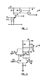
- Fig. 1 of the accompanying drawings shows a basic EFL AND gate 10 as disclosed in U.S. Patent No.3,795,822 to Skokan.
- AND gate 10 has first and second inputs 12 and 14, respectively. Inputs 12 and 14 are coupled to the first and second emitters of an input transistor 16.
- the base of transistor 16 is coupled to a reference voltage 18 and its collector is coupled through a resistor 20 to a supply voltage 22.
- the collector of transistor 16 is also coupled to the base of an output transistor 24.
- the collector of output transistor 24 is also coupled to supply voltage 22.
- Transistor 24 has an emitter coupled to an output 26 which provides the output of the AND gate. Output 26 is a true output, and no complementary output is provided.
- Resistor 20 provides biasing and a transistor 28 prevents saturation of output transistor 24.
- Latch 30 of Figure 2 uses an input transistor 32 which has its base coupled to a data input 34. Its emitter is coupled to a first emitter 36 of a transistor 38, which is similar to transistor 16 of Figure 1.
- Transistor 38 has a collector which provided a true output 40 and is also coupled to the base of an output transistor 42.
- the collector of output transistor 42 is coupled to the collector of input transistor 32 and provides a complementary output 44.
- the collectors of transistors 38 and 42 are coupled to a supply voltage 46 through resistors 48 and 50, respectively.
- a clock input 52 is provided to the base of a transistor 54 which is coupled at its emitter to another transistor 56.
- the base of transistor 56 is coupled to a voltage reference 58.
- the coupled emitters of transistors 54 and 56 are coupled to a current source 60.
- the clock serves to latch the outputs on true and complementary outputs 40 and 44, respectively.
- gate 30 provides both true and-complementary outputs, it can be seen from an examination of the circuit that signals will appear at these outputs at different periods of time after an input is applied to data input 34.
- the true signal on output 40 will not change state until the input signal propagates through transistor 32 and transistor 38.
- the propagation time through transistor 38 is the turn-on time of the transistor.
- the turn-on time is small because it is a minimum geometry device, the capacitive effects are relatively small and its base is at a constant reference D.C. voltage.
- the complementary output 44 will not change state, however, until the signal additionally propagates through transistor 42.
- the time at which outputs appear on the true and complementary outputs varies by an amount equal to the propagation delay through one transistor stage.
- an input transistor has its base coupled to an input and its emitter coupled to an emitter of a reference transistor.
- the reference transistor has its base coupled to a voltage reference and its collector coupled to the base of a true output transistor.
- the emitter of the true output transistor provides the true output, while its collector is coupled to a voltage supply.
- a complementary output transistor has its base coupled to the collector of the input transistor with its emitter providing the complementary output. Its collector is coupled to the voltage supply, as is the collector of the input transistor.
- two emitter-coupled complementary pairs are used.
- the first emitter-coupled pair have their collectors coupled to the emitter of the input transistor and a second emitter of the reference transistor respectively.
- the second emitter of the reference transistor is also coupled to a second emitter of the true output transistor.
- the coupled emitters are connected to a current source.
- the base of one transistor is coupled to a clock input while the base of the other transistor is coupled to a voltage reference.
- the other emitter-coupled transistor pair have their bases and emitters so connected.
- the collector of one transistor is coupled to the voltage supply while the collector of the other transistor is coupled to a second emitter of the complementary output transistor.
- another transistor has its collector coupled to the base of the complementary output transistor, its emitter coupled to the second emitter of the complementary output transistor and its base coupled to the first voltage reference.
- the present invention substantially retains the speed and size advantages of an EFL circuit while providing substantially concurrent complementary and true outputs.
- the present invention thus provides concurrent true and complementary outputs, which previously were only available in emitter coupled logic (ECL) circuits.
- ECL emitter coupled logic
- the present invention requires more area than the prior art gate of Figure 2, but less area than an ECL gate.
- the power consumption is more than that of Figure 2, but less than the power consumption of an ECL gate.
- the speed defined as the time from the input changing state to the slowest output changing state, is faster-for the present invention than the circuit of Figure 2 or a standard ECL gate.
- transistor 74 In operation, when input 72 goes high, transistor 74 is turned on, thereby pulling current through biasing resistor 88 and pulling down the base of transistor 84, thus providing a low level output to complementary output 86.
- transistor 74 For the true output, when transistor 74 is turned on, an emitter 94 of transistor 76 is forced to a high value, thereby limiting the current through the collector of transis,- tor 76 from resistor 90.
- the base of transistor 80 is thus raised to Vcc less the voltage drop across resistor 90, thereby providing a high level output on true output 82.
- the true and complementary outputs will be reversed.
- a clock input 96 is coupled to the base of a transistor 98.
- the emitter of transistor 98 is coupled to the bases of transistors 100 and 102.
- Transistor 102 has its emitter coupled to a transistor 104 and its collector coupled to the emitter of transistor 74.
- Transistor 104 has its collector coupled to a second emitter 122 of reference transistor 76 and a second emitter 120 of output transistor 80.
- the coupled emitters of transistors 102 and 104 are connected to a current source transistor 106.
- the base of transistor 104 is coupled to a second voltage reference level 108.
- transistor 100 has its emitter coupled to the emitter of a transistor 110.
- Transistor 110 has its base coupled to reference voltage 108 and its collector coupled to a second emitter 118 of complementary output transistor 84.
- the collector of transistor 100 is coupled to supply voltage 92.
- a transistor 112 is provided with a collector coupled to the base of complementary output transistor 84 and an emitter coupled to the collector of transistor 110.
- the base of transistor 112 is coupled to first reference voltage 78.
- the circuit also includes current source transistors 114 and 116 and various biasing resistors not mentioned.
- the clock signal falling edge will latch these outputs.
- transistors 100 and 102 are turned off and transistors 104 and 110 are turned on.
- the complementary output 86 is low, the turning on of transistor 110 allows current to flow through transistor 112. This current is pulled through biasing resistor 88 to keep the base of transistor 84 low and thus to keep complementary output 86 low.
- complementary output 86 were high when the clock has its falling edge, current is drawn through second emitter 118 of output transistor 84, but the base of transistor 84 is higher than voltage reference 78, thus keeping transistor 112 turned off.
- transistor 84 This results in the base of transistor 84 remaining at a high level since transistor 112 cannot bring it low and the current into the base of transistor 84 is small, and thus transistor 84 can't develop sufficient voltage across resistor 88 to bring the voltage level at the base of transistor 84 low.
- Transistor 112 and second emitter 118 of transistor 84 thus essentially act as a differential pair, with one or the other being turned on.
- transistors 76 and 80 with second emitter 120 of transistor 80 essentially acting as a differential pair with second emitter 122 of transistor 76.
- the propagation delay for the true output is the delay through input transistor 74, reference transistor 76 and output transistor 80.
- the propagation delay for the complementary output is the delay through input transistor 74 and output transistor 84. Because transistor 76 always has a constant D.C. voltage applied to its base, the Miller capacitance effect of turning on this transistor is minimal. Accordingly, the delay of the true and complementary outputs is equal to approximately the delay through transistors 74 and 80, and transistors 74 and 84, respectively.
- the true output propagation delay is the delay through input transistor 32 and the minimal delay through reference transistor 38.
- the complementary output propagation delay is the delay through transistor 32, the minimal delay through transistor 38 and the delay through transistor 42. The present invention thereby improves the difference between the true and complementary output propagation delays on the order of one transistor propagation delay.
- the present invention may be embodied in other specific forms without departing from the essential characteristics thereof.
- the circuit of Figure 3 could be constructed without the clock and latching mechanism to provide a simple AND gate.
- the present invention could be incorporated into sequential logic which would be compatible with combinational logic.
- the present invention could be incorporated into a master-slave flip-flop which is then coupled to the output of a multiplexer to produce a scan D flip-flop. Accordingly, the disclosure of the preferred embodiment of the invention is intended to be illustrative, but not limiting, of the scope of the invention which is set forth in the following claims.
Landscapes
- Engineering & Computer Science (AREA)
- Power Engineering (AREA)
- Physics & Mathematics (AREA)
- Computer Hardware Design (AREA)
- Computing Systems (AREA)
- General Engineering & Computer Science (AREA)
- Mathematical Physics (AREA)
- Logic Circuits (AREA)
Abstract
Description
- The present invention relates to emitter function logic gates and, in particular, to such gates having complementary outputs.
- Emitter function logic is a class of logic circuit developed for use in large scale integration (LSI) fabrication. Emitter function logic uses less area than other logic circuits by providing only a true output, and not a complementary output. Thus, the requirement of complementing a signal twice to provide a true output as in other logic families is avoided. Therefore, emitter function logic (EFL) is limited to gates which do not require both a true and complementary output. However, by reducing the Miller effect (the multiplication of collector-base feedback capacitance by the voltage gain) and replacing a passive emitter-follower with an active emitter-follower, EFL enjoys an improved speed- power product over ECL (emitter-coupled logic). Modifications of EFL gates to provide complementary outputs have been created, but there is a time delay between the appearance at the output of the true output and the complementary output, thereby limiting the applications.
- Fig. 1 of the accompanying drawings shows a basic EFL AND
gate 10 as disclosed in U.S. Patent No.3,795,822 to Skokan. ANDgate 10 has first andsecond inputs 12 and 14, respectively.Inputs 12 and 14 are coupled to the first and second emitters of aninput transistor 16. The base oftransistor 16 is coupled to areference voltage 18 and its collector is coupled through aresistor 20 to asupply voltage 22. The collector oftransistor 16 is also coupled to the base of anoutput transistor 24. The collector ofoutput transistor 24 is also coupled to supplyvoltage 22.Transistor 24 has an emitter coupled to anoutput 26 which provides the output of the AND gate.Output 26 is a true output, and no complementary output is provided.Resistor 20 provides biasing and atransistor 28 prevents saturation ofoutput transistor 24. - A modified EFL circuit with latched true and complementary outputs is shown in Fig.2 of the accompanying drawings, as disclosed is U.S. Patent No. 4,145,623 to Doucette.
Latch 30 of Figure 2 uses an input transistor 32 which has its base coupled to a data input 34. Its emitter is coupled to afirst emitter 36 of atransistor 38, which is similar totransistor 16 of Figure 1.Transistor 38 has a collector which provided atrue output 40 and is also coupled to the base of anoutput transistor 42. The collector ofoutput transistor 42 is coupled to the collector of input transistor 32 and provides acomplementary output 44. The collectors oftransistors supply voltage 46 throughresistors clock input 52 is provided to the base of atransistor 54 which is coupled at its emitter to anothertransistor 56. The base oftransistor 56 is coupled to avoltage reference 58. The coupled emitters oftransistors current source 60. The clock serves to latch the outputs on true andcomplementary outputs - Although
gate 30 provides both true and-complementary outputs, it can be seen from an examination of the circuit that signals will appear at these outputs at different periods of time after an input is applied to data input 34. The true signal onoutput 40 will not change state until the input signal propagates through transistor 32 andtransistor 38. The propagation time throughtransistor 38 is the turn-on time of the transistor. The turn-on time is small because it is a minimum geometry device, the capacitive effects are relatively small and its base is at a constant reference D.C. voltage. Thecomplementary output 44 will not change state, however, until the signal additionally propagates throughtransistor 42. Thus, the time at which outputs appear on the true and complementary outputs varies by an amount equal to the propagation delay through one transistor stage. - In certain applications, it is desirable to have concurrent true and complementary outputs from an EFL gate without compromising the size and speed advantages of the EFL gate.
- It is an object of the present invention to provide an improved EFL gate which itself provides concurrent true and complementary outputs.
- In accordance with the present invention, an input transistor has its base coupled to an input and its emitter coupled to an emitter of a reference transistor. The reference transistor has its base coupled to a voltage reference and its collector coupled to the base of a true output transistor. The emitter of the true output transistor provides the true output, while its collector is coupled to a voltage supply. A complementary output transistor has its base coupled to the collector of the input transistor with its emitter providing the complementary output. Its collector is coupled to the voltage supply, as is the collector of the input transistor.
- In a preferred embodiment, in order to provide a latched output, two emitter-coupled complementary pairs are used. The first emitter-coupled pair have their collectors coupled to the emitter of the input transistor and a second emitter of the reference transistor respectively. The second emitter of the reference transistor is also coupled to a second emitter of the true output transistor. The coupled emitters are connected to a current source. The base of one transistor is coupled to a clock input while the base of the other transistor is coupled to a voltage reference. Similarly, the other emitter-coupled transistor pair have their bases and emitters so connected. The collector of one transistor is coupled to the voltage supply while the collector of the other transistor is coupled to a second emitter of the complementary output transistor. To provide the latching function, another transistor has its collector coupled to the base of the complementary output transistor, its emitter coupled to the second emitter of the complementary output transistor and its base coupled to the first voltage reference.
- The present invention substantially retains the speed and size advantages of an EFL circuit while providing substantially concurrent complementary and true outputs. The present invention thus provides concurrent true and complementary outputs, which previously were only available in emitter coupled logic (ECL) circuits. The present invention requires more area than the prior art gate of Figure 2, but less area than an ECL gate. Similarly, the power consumption is more than that of Figure 2, but less than the power consumption of an ECL gate. The speed, defined as the time from the input changing state to the slowest output changing state, is faster-for the present invention than the circuit of Figure 2 or a standard ECL gate.
- The invention is described further hereinafter, by way of example only, with reference to the accompanying drawings, in which:
- Figure 1 is schematic diagram of a known EFL AND gate;
- Figure 2 is a schematic diagram of a known D-type latch having both true and complementary outputs; and
- Figure 3 is a schematic diagram of a D-type latch having concurrent true and complementary outputs according to the present invention.
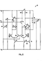
- Figure 3 shows a D-type latch 70 according to the present invention having concurrent true and complementary outputs. A D-input 72 is coupled to the base of an
input transistor 74.Transistor 74 has an emitter coupled to an emitter of areference transistor 76.Transistor 76 has its base coupled to afirst voltage reference 78. The collector oftransistor 76 is coupled to the base of atrue output transistor 80 which has an emitter coupled to atrue output 82. The collector ofinput transistor 74 is coupled to the base of acomplementary output transistor 84. An emitter oftransistor 84 is coupled to a complementary output 86. Biasingresistors transistors Vcc voltage supply 92. - In operation, when input 72 goes high,
transistor 74 is turned on, thereby pulling current through biasingresistor 88 and pulling down the base oftransistor 84, thus providing a low level output to complementary output 86. For the true output, whentransistor 74 is turned on, an emitter 94 oftransistor 76 is forced to a high value, thereby limiting the current through the collector of transis,-tor 76 fromresistor 90. The base oftransistor 80 is thus raised to Vcc less the voltage drop acrossresistor 90, thereby providing a high level output ontrue output 82. For a low level input to input 72, the true and complementary outputs will be reversed. - Additional circuitry is provided to give a clock signal which can latch the outputs. A
clock input 96 is coupled to the base of atransistor 98. The emitter oftransistor 98 is coupled to the bases oftransistors Transistor 102 has its emitter coupled to atransistor 104 and its collector coupled to the emitter oftransistor 74.Transistor 104 has its collector coupled to a second emitter 122 ofreference transistor 76 and asecond emitter 120 ofoutput transistor 80. The coupled emitters oftransistors current source transistor 106. The base oftransistor 104 is coupled to a secondvoltage reference level 108. - Similarly,
transistor 100 has its emitter coupled to the emitter of atransistor 110.Transistor 110 has its base coupled toreference voltage 108 and its collector coupled to asecond emitter 118 ofcomplementary output transistor 84. The collector oftransistor 100 is coupled to supplyvoltage 92. Atransistor 112 is provided with a collector coupled to the base ofcomplementary output transistor 84 and an emitter coupled to the collector oftransistor 110. The base oftransistor 112 is coupled tofirst reference voltage 78. - The circuit also includes
current source transistors - In operation, when the positive edge of a clock input is applied to
clock input 96, the level of the emitter oftransistor 98 is raised, thereby providing a high voltage level to the bases oftransistors input transistor 74 so that a subsequent input signal can propagate to the output. Simultaneously,transistors - After the input has been provided to the appropriate outputs, the clock signal falling edge will latch these outputs. When the clock goes low,
transistors transistors transistor 110 allows current to flow throughtransistor 112. This current is pulled through biasingresistor 88 to keep the base oftransistor 84 low and thus to keep complementary output 86 low. Conversely, if complementary output 86 were high when the clock has its falling edge, current is drawn throughsecond emitter 118 ofoutput transistor 84, but the base oftransistor 84 is higher thanvoltage reference 78, thus keepingtransistor 112 turned off. This results in the base oftransistor 84 remaining at a high level sincetransistor 112 cannot bring it low and the current into the base oftransistor 84 is small, and thustransistor 84 can't develop sufficient voltage acrossresistor 88 to bring the voltage level at the base oftransistor 84 low.Transistor 112 andsecond emitter 118 oftransistor 84 thus essentially act as a differential pair, with one or the other being turned on. - A similar result is obtained from
transistors second emitter 120 oftransistor 80 essentially acting as a differential pair with second emitter 122 oftransistor 76. - As can be seen, the propagation delay for the true output is the delay through
input transistor 74,reference transistor 76 andoutput transistor 80. The propagation delay for the complementary output is the delay throughinput transistor 74 andoutput transistor 84. Becausetransistor 76 always has a constant D.C. voltage applied to its base, the Miller capacitance effect of turning on this transistor is minimal. Accordingly, the delay of the true and complementary outputs is equal to approximately the delay throughtransistors transistors reference transistor 38. The complementary output propagation delay, on the other hand, is the delay through transistor 32, the minimal delay throughtransistor 38 and the delay throughtransistor 42. The present invention thereby improves the difference between the true and complementary output propagation delays on the order of one transistor propagation delay. - As will be understood by those familiar with the art, the present invention may be embodied in other specific forms without departing from the essential characteristics thereof. For example, although less desirable, the circuit of Figure 3 could be constructed without the clock and latching mechanism to provide a simple AND gate. Alternately, the present invention could be incorporated into sequential logic which would be compatible with combinational logic. For example, the present invention could be incorporated into a master-slave flip-flop which is then coupled to the output of a multiplexer to produce a scan D flip-flop. Accordingly, the disclosure of the preferred embodiment of the invention is intended to be illustrative, but not limiting, of the scope of the invention which is set forth in the following claims.
Claims (6)
Applications Claiming Priority (2)
| Application Number | Priority Date | Filing Date | Title |
|---|---|---|---|
| US06/942,669 US4728818A (en) | 1986-12-17 | 1986-12-17 | Emitter function logic with concurrent, complementary outputs |
| US942669 | 1986-12-17 |
Publications (2)
| Publication Number | Publication Date |
|---|---|
| EP0272011A2 true EP0272011A2 (en) | 1988-06-22 |
| EP0272011A3 EP0272011A3 (en) | 1989-10-25 |
Family
ID=25478437
Family Applications (1)
| Application Number | Title | Priority Date | Filing Date |
|---|---|---|---|
| EP87310438A Withdrawn EP0272011A3 (en) | 1986-12-17 | 1987-11-26 | Emitter function logic with concurrent, complementary outputs |
Country Status (4)
| Country | Link |
|---|---|
| US (1) | US4728818A (en) |
| EP (1) | EP0272011A3 (en) |
| JP (1) | JPS63166312A (en) |
| AU (1) | AU589307B2 (en) |
Cited By (1)
| Publication number | Priority date | Publication date | Assignee | Title |
|---|---|---|---|---|
| WO1997021270A1 (en) * | 1995-12-07 | 1997-06-12 | Northern Telecom Limited | Serial multi-gb/s data receiver |
Families Citing this family (1)
| Publication number | Priority date | Publication date | Assignee | Title |
|---|---|---|---|---|
| US4894562A (en) * | 1988-10-03 | 1990-01-16 | International Business Machines Corporation | Current switch logic circuit with controlled output signal levels |
Family Cites Families (8)
| Publication number | Priority date | Publication date | Assignee | Title |
|---|---|---|---|---|
| JPS4930592A (en) * | 1972-06-08 | 1974-03-19 | ||
| US3795822A (en) * | 1972-08-14 | 1974-03-05 | Hewlett Packard Co | Multiemitter coupled logic gate |
| DE2247189C3 (en) * | 1972-09-26 | 1978-11-09 | Siemens Ag, 1000 Berlin Und 8000 Muenchen | Bistable switching element for flip-flop circuits in ECL circuit technology |
| US4145623A (en) * | 1977-10-04 | 1979-03-20 | Burroughs Corporation | Current mode logic compatible emitter function type logic family |
| US4378505A (en) * | 1980-09-29 | 1983-03-29 | Bell Telephone Laboratories, Inc. | Emitter function logic latch and counter circuits |
| US4357547A (en) * | 1981-02-23 | 1982-11-02 | Motorola, Inc. | EFL Toggle flip-flop |
| US4506171A (en) * | 1982-12-29 | 1985-03-19 | Westinghouse Electric Corp. | Latching type comparator |
| US4647799A (en) * | 1984-06-29 | 1987-03-03 | Advanced Micro Devices, Inc. | Full and fractional swing with adjustable high level ECL gate using a single current source |
-
1986
- 1986-12-17 US US06/942,669 patent/US4728818A/en not_active Expired - Lifetime
-
1987
- 1987-11-26 EP EP87310438A patent/EP0272011A3/en not_active Withdrawn
- 1987-12-16 AU AU82628/87A patent/AU589307B2/en not_active Ceased
- 1987-12-17 JP JP62320063A patent/JPS63166312A/en active Pending
Cited By (2)
| Publication number | Priority date | Publication date | Assignee | Title |
|---|---|---|---|---|
| WO1997021270A1 (en) * | 1995-12-07 | 1997-06-12 | Northern Telecom Limited | Serial multi-gb/s data receiver |
| US5852637A (en) * | 1995-12-07 | 1998-12-22 | Northern Telecom Limited | Serial multi-GB/s data receiver |
Also Published As
| Publication number | Publication date |
|---|---|
| EP0272011A3 (en) | 1989-10-25 |
| AU589307B2 (en) | 1989-10-05 |
| AU8262887A (en) | 1988-06-23 |
| US4728818A (en) | 1988-03-01 |
| JPS63166312A (en) | 1988-07-09 |
Similar Documents
| Publication | Publication Date | Title |
|---|---|---|
| EP0168231A2 (en) | A combination circuit | |
| US4333020A (en) | MOS Latch circuit | |
| US5148061A (en) | ECL to CMOS translation and latch logic circuit | |
| US5900745A (en) | Semiconductor device including input buffer circuit capable of amplifying input signal with low amplitude in high speed and under low current consumption | |
| US4577125A (en) | Output voltage driver with transient active pull-down | |
| US5900760A (en) | Low voltage ECL latch and flip-flop | |
| US5485110A (en) | ECL differential multiplexing circuit | |
| US4728818A (en) | Emitter function logic with concurrent, complementary outputs | |
| KR19990057768A (en) | Schmitt trigger circuit | |
| US4349753A (en) | Emitter function logic flip-flop circuit | |
| JPH0736507B2 (en) | Semiconductor logic circuit | |
| US4357547A (en) | EFL Toggle flip-flop | |
| EP0875997A2 (en) | A BiCMOS logic gate | |
| JPH02268515A (en) | Bi-cmos logic circuit | |
| JP3487631B2 (en) | Electronic circuit with driver circuit | |
| US4398103A (en) | Enabling circuitry for logic circuits | |
| JP2880298B2 (en) | BiCMOS multiplexer and logic gate and adder using the same | |
| JP3778566B2 (en) | Low voltage BiCMOS digital delay chain suitable for operation over a wide power supply range | |
| US4277698A (en) | Delay type flip-flop | |
| JP2834208B2 (en) | Semiconductor integrated circuit device | |
| JP2681937B2 (en) | Flip flop | |
| JPH01286511A (en) | Master slave type flip-flop circuit | |
| JPH0239719A (en) | Semiconductor circuit | |
| KR0113957Y1 (en) | Circuit for driving internal 3-state bus | |
| JPH05268032A (en) | Semiconductor integrated circuit device |
Legal Events
| Date | Code | Title | Description |
|---|---|---|---|
| PUAI | Public reference made under article 153(3) epc to a published international application that has entered the european phase |
Free format text: ORIGINAL CODE: 0009012 |
|
| AK | Designated contracting states |
Kind code of ref document: A2 Designated state(s): DE FR GB IT SE |
|
| PUAL | Search report despatched |
Free format text: ORIGINAL CODE: 0009013 |
|
| AK | Designated contracting states |
Kind code of ref document: A3 Designated state(s): DE FR GB IT SE |
|
| 17P | Request for examination filed |
Effective date: 19900316 |
|
| 17Q | First examination report despatched |
Effective date: 19900831 |
|
| STAA | Information on the status of an ep patent application or granted ep patent |
Free format text: STATUS: THE APPLICATION IS DEEMED TO BE WITHDRAWN |
|
| 18D | Application deemed to be withdrawn |
Effective date: 19910903 |
|
| RIN1 | Information on inventor provided before grant (corrected) |
Inventor name: CHENGSON, DAVID P. Inventor name: KHAN, AURANGZEB K. |