EP0271202A2 - Triggerschaltung für ein Oszilloskop - Google Patents
Triggerschaltung für ein Oszilloskop Download PDFInfo
- Publication number
- EP0271202A2 EP0271202A2 EP87309682A EP87309682A EP0271202A2 EP 0271202 A2 EP0271202 A2 EP 0271202A2 EP 87309682 A EP87309682 A EP 87309682A EP 87309682 A EP87309682 A EP 87309682A EP 0271202 A2 EP0271202 A2 EP 0271202A2
- Authority
- EP
- European Patent Office
- Prior art keywords
- trigger
- amplifier
- gain
- input
- gain control
- Prior art date
- Legal status (The legal status is an assumption and is not a legal conclusion. Google has not performed a legal analysis and makes no representation as to the accuracy of the status listed.)
- Withdrawn
Links
- 229920005994 diacetyl cellulose Polymers 0.000 claims 1
- 230000001960 triggered effect Effects 0.000 description 2
- 238000006243 chemical reaction Methods 0.000 description 1
- 230000000694 effects Effects 0.000 description 1
- 238000005070 sampling Methods 0.000 description 1
- 230000011664 signaling Effects 0.000 description 1
Images


Classifications
-
- G—PHYSICS
- G01—MEASURING; TESTING
- G01R—MEASURING ELECTRIC VARIABLES; MEASURING MAGNETIC VARIABLES
- G01R13/00—Arrangements for displaying electric variables or waveforms
- G01R13/20—Cathode-ray oscilloscopes
- G01R13/22—Circuits therefor
- G01R13/32—Circuits for displaying non-recurrent functions such as transients; Circuits for triggering; Circuits for synchronisation; Circuits for time-base expansion
Definitions
- An oscilloscope is used to acquire, analyze and display electronic signal waveforms.
- the oscilloscope takes electronic signals and plots their waveforms on a cathode ray tube (CRT) display screen in units of voltage-versus-time.
- CRT cathode ray tube
- voltage amplitude is plotted along the vertical, that is, the Y axis
- time is plotted along the horizontal, that is, the X axis.
- digital oscilloscopes have been developed.
- the basic scheme in digital oscilloscope operation is the sampling of a signal followed by analog-to-digital conversion of the voltage values of the acquired samples. The digitized information is then placed in memory and used to create the display of the signal's waveform.
- a trigger level is a voltage value which the input signal must exceed before the oscilloscope begins tracking the signal with samples.
- the oscilloscope is said to be triggered when this level is achieved.
- Double triggering is an error caused by a so-called false trigger.
- a false trigger is noise on the input signal which may appear as a trigger voltage level to the triggering circuitry of the oscilloscope.
- Double triggering can result in the appearance of two superimposed and out-of-phase versions of the same signal on the oscilloscope display screen.
- hysteresis is introduced into the trigger circuit of the oscilloscope. Fundamentally, hysteresis is just the difference between two voltage levels.
- the hysteresis defines a first voltage level, known as the arm point, and a second higher voltage level, known as the fire point.
- the input signal must first exceed the arm point and then the fire point, in sequence, in order for the trigger circuit to detect a true trigger.
- the arm point can enable a trigger comparator and the fire point can cause an output from the trigger comparator, signalling a true trigger.
- the hysteresis is set such that typical signal noise and internal instrument noise will not cause a false trigger.
- the size of the hysteresis determines the minimum signal necessary to produce a triggered waveform on the oscilloscope display screen.
- Figure 1 shows an input signal having an arm point and a fire point defining the triggering hyteresis, where the hysteresis is the fire point value minus the arm point value.
- Figure 2 shows an input signal having a false trigger due to noise on the signal.
- Figure 3 shows an example of the double trigger display which is due to a false trigger.
- FIG. 4 shows a typical oscilloscope circuit wherein input signal 50 is buffered by buffer amplifier 110 and then sent to both a vertical gain vernier circuit 75 and trigger circuit 100.
- Vertical gain circuit 75 comprises a vertical amplifier 120 which controls the gain vernier along the vertical axis, that is, the voltage ampltiude axis, of the oscilloscope display screen.
- Vertical amplifier 120 has a user-adjustable vertical gain vernier control 125, typically having a range of 1 through 2.5.
- Trigger circuit 100 comprises a trigger amplifier 130 and a trigger comparator 140.
- One input to trigger comparator 140 is the output of trigger amplifier 130.
- the other input to trigger comparator 140 is a user-adjustable trigger level input having trigger level offset control 145.
- the trigger level input defines the voltage level at which the oscilloscope will trigger.
- Trigger comparator 140 will produce an output given a predetermined difference between its inputs.
- the output of trigger comparator 140 indicates a true trigger.
- trigger comparator 140 has a fixed hysteresis.
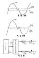
- trigger amplifier 130 has a gain control 135. Varying the gain of trigger amplifier 130 varies the input to trigger comparator 140 and consequently the effective hysteresis is varied. For instance, with a fixed hysteresis on trigger comparator 140, a doubling of the output of trigger amp 130 will halve the hysteresis and a halving of the output of trigger amplifier 130 will double the hysteresis. This variation in the effective hysteresis can be seen in Figures 5A and 5B. In Figure 5A, input signal 25A has a noise spike on its down slope but the size of the hysteresis prevents a false trigger.
- the gain control 135 of trigger amplifier 130 is typically fixed when the instrument in calibrated. However, fixing the trigger amplifier gain has negative side-effects. To keep a signal spanned across a constant number of divisions on the display screen as the vertical gain 125 is adjusted from X1 to X2.5, the input to trigger amplifier 130 would also have to vary from X1 to X2.5, causing the hysteresis to vary inversely, requiring trigger level control 145 to have sufficient range to cover the largest signal at the lowest vertical gain setting as well as sufficient resolution to cover the smallest signal at the largest vertical gain setting. The slew rate demands through the trigger circuit path would also be X2.5 higher than if the signal range was fixed.
- the present invention provides for an effective constant hysteresis through a micro-processor controlled tracking of the trigger amplifier gain control and the vertical amplfier gain control.
- a micro-processor controls the tracking of the two gain controls via digital-to-analog converters (DAC) which are connected to the input of each gain control.
- DAC digital-to-analog converters
- the tracking of the two gain controls allows for an effectively constant voltage range input to the trigger comparator relative to the on-screen vertical range of the signal.
- DAC digital-to-analog converters
- Figure 6 shows a circuit for tracking the trigger amplifier gain control 135 to the vertical amplifier gain control 125.
- the oscilloscope user can enter vertical gain control commands at keyboard 200.
- Microprocessor 205 then issues predetermined signals to vertical gain control 125 via digital-to-analog convertor (DAC) 210 and to trigger gain control 135 via DAC 220.
- DAC digital-to-analog convertor
- the tracking by microporcessor 205 serves to inversely adjust trigger amplifier gain control 135 relative to vertical gain control 125 such that the effective hysteresis seen by trigger comparator 140 remains constant.
Landscapes
- Physics & Mathematics (AREA)
- General Physics & Mathematics (AREA)
- Control Of Amplification And Gain Control (AREA)
- Manipulation Of Pulses (AREA)
Applications Claiming Priority (2)
| Application Number | Priority Date | Filing Date | Title |
|---|---|---|---|
| US92893686A | 1986-11-10 | 1986-11-10 | |
| US928936 | 1986-11-10 |
Publications (2)
| Publication Number | Publication Date |
|---|---|
| EP0271202A2 true EP0271202A2 (de) | 1988-06-15 |
| EP0271202A3 EP0271202A3 (de) | 1989-12-13 |
Family
ID=25457043
Family Applications (1)
| Application Number | Title | Priority Date | Filing Date |
|---|---|---|---|
| EP87309682A Withdrawn EP0271202A3 (de) | 1986-11-10 | 1987-11-02 | Triggerschaltung für ein Oszilloskop |
Country Status (2)
| Country | Link |
|---|---|
| EP (1) | EP0271202A3 (de) |
| JP (1) | JPS63132175A (de) |
Cited By (1)
| Publication number | Priority date | Publication date | Assignee | Title |
|---|---|---|---|---|
| EP0663597A3 (de) * | 1994-01-13 | 1997-03-05 | Fluke Corp | Triggerschaltung mit zwei Komparatoren und unabhängige Spannungsabstimmung. |
Family Cites Families (2)
| Publication number | Priority date | Publication date | Assignee | Title |
|---|---|---|---|---|
| US4225940A (en) * | 1978-10-02 | 1980-09-30 | Tektronix, Inc. | Oscilloscope system for acquiring, processing, and displaying information |
| US4555765A (en) * | 1982-09-14 | 1985-11-26 | Analogic Corporation | Multi-mode oscilloscope trigger with compensating trigger delay |
-
1987
- 1987-11-02 EP EP87309682A patent/EP0271202A3/de not_active Withdrawn
- 1987-11-10 JP JP28513087A patent/JPS63132175A/ja active Pending
Cited By (1)
| Publication number | Priority date | Publication date | Assignee | Title |
|---|---|---|---|---|
| EP0663597A3 (de) * | 1994-01-13 | 1997-03-05 | Fluke Corp | Triggerschaltung mit zwei Komparatoren und unabhängige Spannungsabstimmung. |
Also Published As
| Publication number | Publication date |
|---|---|
| JPS63132175A (ja) | 1988-06-04 |
| EP0271202A3 (de) | 1989-12-13 |
Similar Documents
| Publication | Publication Date | Title |
|---|---|---|
| US4283713A (en) | Waveform acquisition circuit | |
| US4736189A (en) | Method and apparatus for calibrating an analog-to-digital conversion apparatus | |
| US5870051A (en) | Method and apparatus for analog signal conditioner for high speed, digital x-ray spectrometer | |
| US4611164A (en) | Spectrum analyzer with automatic peak frequency tuning function | |
| EP0225705A2 (de) | Methode und Einrichtung zur Sammlung von zeitabhängigen Daten | |
| EP0158802A1 (de) | Digitales Erfassungssystem mit schnellem Abtasttor | |
| EP0174151B1 (de) | Verzögertes Triggersystem für ein Digital-Oszilloskop | |
| US3893036A (en) | Precision function generator | |
| US5414635A (en) | Oscilloscope with dynamic triggering determination | |
| US6348886B1 (en) | Self-calibrating video digital to analog converter | |
| CA1213947A (en) | Signal conditioner for biological signals | |
| US4238727A (en) | Digitally programmable apparatus for generating a substantially linear ramp signal | |
| US4254406A (en) | Integrating analog-to-digital converter | |
| US4823077A (en) | Channel-gain-vernier-tracking trigger hysteresis for an oscilloscope | |
| EP0271202A2 (de) | Triggerschaltung für ein Oszilloskop | |
| US4769613A (en) | Digitalized amplitude detection circuit for analog input signal | |
| EP0004152A1 (de) | Digitalumwandlung eines periodischen Analog-Signals | |
| US4734677A (en) | Coarse/fine A-D converter using ramp waveform to generate fine digital signal | |
| US4717883A (en) | Method and apparatus for reducing errors in a sampling system utilizing an error-sampled feedback loop | |
| US4804939A (en) | Coarse/fine A-D converter using ramp waveform to generate fine digital signal | |
| EP0185096B1 (de) | Vorrichtung zum steuern der amplitüde senkrecht abweichender signale | |
| US4989005A (en) | Method of analog/digital conversion | |
| KR100299247B1 (ko) | 펄스신호분석장치 | |
| GB2068694A (en) | Slide-back waveform analyzer | |
| SU1500827A2 (ru) | Устройство регистрации с автоматической калибровкой |
Legal Events
| Date | Code | Title | Description |
|---|---|---|---|
| PUAI | Public reference made under article 153(3) epc to a published international application that has entered the european phase |
Free format text: ORIGINAL CODE: 0009012 |
|
| AK | Designated contracting states |
Kind code of ref document: A2 Designated state(s): DE FR GB |
|
| PUAL | Search report despatched |
Free format text: ORIGINAL CODE: 0009013 |
|
| AK | Designated contracting states |
Kind code of ref document: A3 Designated state(s): DE FR GB |
|
| RHK1 | Main classification (correction) |
Ipc: G01R 13/22 |
|
| 17P | Request for examination filed |
Effective date: 19900420 |
|
| 17Q | First examination report despatched |
Effective date: 19920115 |
|
| STAA | Information on the status of an ep patent application or granted ep patent |
Free format text: STATUS: THE APPLICATION IS DEEMED TO BE WITHDRAWN |
|
| 18D | Application deemed to be withdrawn |
Effective date: 19920728 |
|
| RIN1 | Information on inventor provided before grant (corrected) |
Inventor name: HANCOCK, JOHNNIE L. Inventor name: LANDGRAF, ROBERT M. |