EP0264884B2 - Key input device - Google Patents
Key input device Download PDFInfo
- Publication number
- EP0264884B2 EP0264884B2 EP87115277A EP87115277A EP0264884B2 EP 0264884 B2 EP0264884 B2 EP 0264884B2 EP 87115277 A EP87115277 A EP 87115277A EP 87115277 A EP87115277 A EP 87115277A EP 0264884 B2 EP0264884 B2 EP 0264884B2
- Authority
- EP
- European Patent Office
- Prior art keywords
- contact
- sheet
- microcomputer
- key
- groups
- Prior art date
- Legal status (The legal status is an assumption and is not a legal conclusion. Google has not performed a legal analysis and makes no representation as to the accuracy of the status listed.)
- Expired - Lifetime
Links
Images


Classifications
-
- H—ELECTRICITY
- H03—ELECTRONIC CIRCUITRY
- H03M—CODING; DECODING; CODE CONVERSION IN GENERAL
- H03M11/00—Coding in connection with keyboards or like devices, i.e. coding of the position of operated keys
- H03M11/22—Static coding
- H03M11/24—Static coding using analogue means, e.g. by coding the states of multiple switches into a single multi-level analogue signal or by indicating the type of a device using the voltage level at a specific tap of a resistive divider
Definitions
- the present invention relates to a key input device so designed that the kind of a key depressed is determined by the combined use of an analog-type signal and a digital-type signal.
- This type of system includes a plurality of output ports and a plurality of ordinary input terminals so that scan pulses of a controlled timing are generated from the output ports and the corresponding pulse is applied to the input terminal connected to the depressed key, thereby discriminating the key.
- this system is also not a method which drastically decreases the number of the required input and output terminals and therefore it is limited by the number of the input and output terminals of the microcomputer.
- these input and output terminals are used only for operating key inputting purposes, there is a shortage of the input and output terminals for the other essential control purposes.
- it leads to a pressure for the capacity of the ROM of the microcomputer used with this system for scan output control purposes. etc.
- this system is of an analog-to-digital conversion (AID conversion) type in which voltages generated by the depression of the respective keys differ from one another in accordance with their kinds and each key is discriminated by converting the corresponding analog voltage to digital form.
- AID conversion analog-to-digital conversion
- US-A-4,015,254 essentially discloses key input devices as shown in present Fig. 1A and 1B, respectively.
- DE-A-33 38 749 discloses a key input device, in which according to Fig. 3 thereof a microcomputer receives both, digital and analog signals at respective input terminals. There are provided first keys for applying said digital signals to the microcomputer and second keys for applying said analog signals to said microcomputer. The discrimination of the keys for applying said analog signals is performed on the basis of both, the analog and the digital signals. The digital signals serve for providing a second function for each of said keys for applying said analog signals.
- Figs. 1A and 1B are diagrams showing conventional key input systems.
- Fig. 2 is an extemal view of a high-frequency heating apparatus incorporating an embodiment of the invention.
- Fig. 3 is a circuit diagram of the apparatus of Fig. 2.
- Fig. 4 is a diagram showing a detailed construction of one key input portion in the embodiment of Fig. 2.
- Fig. 5 is a sectional view for explaining the operation of one key input portion in the embodiment of Fig. 2.
- Fig. 6 is a diagram showing the construction of the key input section in the embodiment of Fig. 2.
- Fig. 7 is a diagram for explaining the control of the embodiment of Fig. 2.
- Fig. 8 is a diagram showing the construction of a key input section in a modification of the embodiment of Fig. 2.
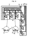
- Fig. 9 is a pattern diagram of the key input section in the embodiment of Fig. 2.
- Fig. 10 is a pattern diagram of a key input section in another modification of the embodiment of Fig. 2.
- Numeral 1 designates the body of a high-frequency heating apparatus.
- a heating chamber 2 is formed inside the body 1.
- Numeral 3 designates a hinged door fitted in the opening of the heating chamber 2, and 4 a control panel arranged on the front part of the body 1 to allow the user to set a cooking sequence such as cooking power and time.
- the control panel 4 contains a control circuit unit 5 including a microcomputer and a keyboard 6 for feeding the intention of the user into the microcomputer.
- the microcomputer 5a shown in Fig. 3 performs and controls the cooking sequence in accordance with the preprogrammed contents.
- Fig. 3 shows a circuit diagram for the apparatus of Fig. 2.
- the apparatus includes a magnetron 7 serving as a high-frequency oscillator, a transformer 8 for supplying power to the magnetron 7, and switches 9a and 9b for switching on and off the power supplied to the transformer 8 to switch on and off the high-frequency output of the magnetron 7.
- the microcomputer 5a includes ordinary input terminals K 1 to K 4 and an A/D conversion input terminal A/D 1 and the terminals are wired in correspondence to the respective keys of the keyboard 6. Also connected to the keyboard 6 is a + voltage (+ 5 V) which serves as a power supply for the microcomputer 5a and as an A/D conversion input power supply.
- the keyboard 6 includes a plurality of keys such as cooking power keys, cooking time keys and a start key and each of the keys has a separate switch function. These switch functions serve to open and close the circuits of the input terminals (K 1 ⁇ K 4 , A/D 1 ) of the microcomputer 5a.
- Numeral 10 designates a panel showing the positions of the keys and providing an external appearance.
- the panel 10 is designed so that it can be recognized easily by the user.
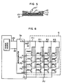
- Numeral 11 designates a conductive sheet forming contacts for the switch functions, 12a spacer providing contact gaps, arranged to ensure the insulation for those portions other than the contact portions of the keys and also formed with an opening at its portions corresponding to each contact portion to cause the conductive sheet 11 to directly face the openings, and 13 a pattem sheet having a plurality of contact patterns formed thereon to touch the conductive sheet 11 through the spacer 12 in response to the depression of the respective keys.
- a reinforcing sheet 14 is provided to reinforce the whole assembly.
- the conductive sheet 11 is connected to the metal portion of the high-frequency heating apparatus body with small screws or the like and the control circuit unit 5 is similarly connected electrically to the heating apparatus body, thereby connecting the 5-volt power supply of the microcomputer 5a to the conductive sheet 11 of the keyboard 6 through the metal portion of the heating apparatus body.
- Fig. 6 showing a connection diagram for the patterns on the pattern sheet 13 of the keyboard 6 and the microcomputer 5a.
- the keys include 16 different ones so that if, for example, the POWER key is depressed, the voltage of 5 V is applied to the ordinary input terminal K 1 of the microcomputer 5a by the pattern P2 of Fig. 6 and also the divided voltage by ladder resister R 1 , R 2 , R 3 and R x is applied to the A/D conversion input terminal A/D 1 through the pattern P 1 .
- the keys include 16 different ones so that if, for example, the POWER key is depressed, the voltage of 5 V is applied to the ordinary input terminal K 1 of the microcomputer 5a by the pattern P2 of Fig. 6 and also the divided voltage by ladder resister R 1 , R 2 , R 3 and R x is applied to the A/D conversion input terminal A/D 1 through the pattern P 1 .
- the keys include 16 different ones so that if, for example, the POWER key is depressed, the voltage of 5 V is
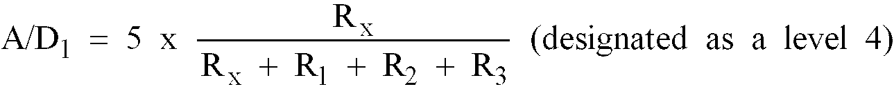
- the resolution of this ladder circuit is selectively set to four levels and therefore the voltage applied to the microcomputer 5a through the input terminal A/D 1 changes in response to the depression of the respective keys as follows.
- A/D 1 5 V (designated as a level 1)
- A/D 1 5 x R x R x + R 1 (designated as a level 2)
- A/D 1 5 x R x R x + R 1 + R 2 (designated as a level 3)
- A/D 1 5 x R x R x + R 1 + R 2 + R 3 (designated as a level 4)
- the keys are also connected in groups of four keys each to the ordinary input terminals K 1 , K 2 , K 3 and K 4 , respectively, and the matrix table of Fig. 7 is prepared in accordance with the various combinations of two input signals.
- the microcomputer 5a discriminates each key in accordance with the corresponding combination of two different input signals.
- the POWER key corresponds to the level 1 and the associated input is a K 1 input.
- the key S 33 corresponds to the level 3 and the associated input is a K 3 input.
- the microcomputer 5a determines first the kind of the ordinary input (K 1 ⁇ K 4 ) and it then determines the level of the A/D conversion input, thereby determining the kind of the depressed key.
- the POWER, S 12 , S 13 and S 14 keys, connected to the voltage of the level 1 are each placed in the preferential position in the corresponding row. For instance, when the POWER and S 21 keys are depressed simultaneously, the voltage of the level 1 is generated at the A/D 1 terminal and the smaller the level number the higher the priority level is. Therefore, the preferential keys can be attained by simply determining the corresponding matrix positions and there is no need to increase the ROM capacity and the RAM capacity for any program.
- the key scanning input terminals of the microcomputer 5a can be reduced as compared with the conventional key matrix system and also any increased number of the keys on the keyboard can be easily met with by increasing the AID resolution levels for AID conversion inputs.
- the output terminals of the microcomputer 5a are ensured amply and therefore the degree of freedom of designing is increased from the program designing standpoint of the microcomputer 5a with the resulting effect of causing some superfluous portion in the ROM capacity of the microcomputer 5a and allowing additional utilization thereof.
- the application of voltage to the patterns is effected only when any key is depressed and therefore the invention is advantageous with respect to the problem of interpattern migration which is encountered in the construction of the actual membrane.
- the embodiment only the reduced resolution levels are required for the A/D conversion resolution and this is a great advantage from the accuracy standpoint of forming a resistor pattern on the actual membrane.
- FIG. 8 a second embodiment of the invention will be described.
- This embodiment shows a case in which the number of keys is increased by two times by simply adding a single A/D conversion input terminal.
- the number of keys can be doubled by combining the similar matrix with the additional AID conversion input terminal and using the same ordinary input terminals K 1 and K 2 without any addition.
- the corresponding key discrimination table is as shown in Fig. 8. Also, the same dividing resistors R 1 , R 2 , R 3 and R x for A/D conversion may be used for the terminals A/D 1 and A/D 2 or the dividing resistors for the two may be different from each other, and the provision of these dividing resistors can be realized easily.
- the pattern P 1 and the patterns P 2 , P 3 , P 4 , and P 5 are respectively arranged in comb form.
- the group of ladder resistors R 1 , R 2 and R 3 prepared by, for example, forming carbon to the desired thickness, width, etc., to provide a high resistance value can be formed on a part of the pattern P 1 by the same operation as the other patterns. Since the present invention requires no increase in the resolution of the ladder resistors, the precision attained by this carbon resistor method can be considered sufficient for the ladder resistors.
- these resistors can be easily attained by the operation of printing and baking carbon on the pattern sheet 13.
- the resistance value can be increased by decreasing the width of the carbon pattern and conversely the resistance value can be reduced by increasing the width of the carbon pattern.
- the patterns other than the resistors R 1 , R 2 and R 3 may be formed with carbon mixed with such material as silver, thereby producing pattems having a very small resistance value.
- a resist RG is placed at each of the points where the patterns overlap one another to prevent the patterns from contacting with one another.
- the provision of the ladder resistor group of R 1 , R 2 and R 3 of a high resistance value and the pattems P 1 , P 2 , P 3 , P 4 , and P 5 of a low resistance value and the provision of the resist portions RG at the pattern intersections can be easily effected.
- the construction of this invention has the effect of greatly improving the quality in that excepting when any key is depressed so that the conductive sheet 11 supplied with 5 V is brought into contact with the pattem sheet 13 through the spacer sheet 12, no voltage is applied to the patterns on the pattern sheet 13 and the A/D conversion pattern P 1 and the ordinary input patterns P 2 , P 3 , P 4 and P 5 are all at the same potential, thereby preventing the occurrence of migration caused in the silver material which has been used frequently for such patterns.
- a pattem PV connected to the 5-volt power supply is formed as a third contact pattern on the pattem sheet 13, and the conductive sheet 11 simply forms a conductive film which is supplied with no voltage.
Description
- The present invention relates to a key input device so designed that the kind of a key depressed is determined by the combined use of an analog-type signal and a digital-type signal.
- The recent development in the field of semiconductors has been so remarkable that the construction of control systems with electronic circuits has advanced rapidly. Thus, the constructions of control systems and the shapes of control panels have undergone considerable changes and the constructions of their input means have also undergone changeover from the mechanical switches mainly to those types which discriminates the respective keys by means of a microcomputer through the medium of electric signals, thereby performing the control.
- In addition, a wave of this digitization has resulted in the addition of new functions one after another and the trend has been toward increasing the number of operating keys for effecting such functions.
- However, the increase in the number of such keys has resulted In an increase in the input and output terminals of the microcomputer and hence the number of peripheral circuits has been increased from the construction standpoint of the system.
- In view of these circumstances, as shown in Fig. 1A of the accomoanying drawings, attempts heretofore made to decrease the number of input and output terminals increasing in proportion to an increase in the number of operating keys has been mainly of a key-scan matrix type in which a matrix circuit is formed by an output signal system and an input signal system so as to discriminate the kinds of the respective depressed keys with the reduced inputs and outputs.
- This type of system includes a plurality of output ports and a plurality of ordinary input terminals so that scan pulses of a controlled timing are generated from the output ports and the corresponding pulse is applied to the input terminal connected to the depressed key, thereby discriminating the key.
- However, this system is also not a method which drastically decreases the number of the required input and output terminals and therefore it is limited by the number of the input and output terminals of the microcomputer. Thus, if these input and output terminals are used only for operating key inputting purposes, there is a shortage of the input and output terminals for the other essential control purposes. Moreover, it leads to a pressure for the capacity of the ROM of the microcomputer used with this system for scan output control purposes. etc.
- Also, as another example of the conventional methods, there has been a system which utilizes analog inputs. As shown in Fig. 1B, this system is of an analog-to-digital conversion (AID conversion) type in which voltages generated by the depression of the respective keys differ from one another in accordance with their kinds and each key is discriminated by converting the corresponding analog voltage to digital form.
- Since this system includes an AID conversion input terminal and each key is discriminated in accordance with a variation in the voltage generated by its depression, when the key at the fifth row from above in Fig. 1B is depressed. the following voltage is generated

- However, this system is also disadvantageous in that an increase in the number of keys requires a resolution for the AID conversion and therefore it is necessary to use high-precision resistors for generating a voltage corresponding to each key, thus making the system unfavorable from the standpoint of cost and working performance.
- US-A-4,015,254 essentially discloses key input devices as shown in present Fig. 1A and 1B, respectively.
- DE-A-33 38 749 discloses a key input device, in which according to Fig. 3 thereof a microcomputer receives both, digital and analog signals at respective input terminals. There are provided first keys for applying said digital signals to the microcomputer and second keys for applying said analog signals to said microcomputer. The discrimination of the keys for applying said analog signals is performed on the basis of both, the analog and the digital signals. The digital signals serve for providing a second function for each of said keys for applying said analog signals.
- In view of the background as mentioned above, it is an object of the present invention to provide an effective key input device so designed that operating key inputs are taken in by a novel means combining the A/D conversion system and the matrix system.
- It is another object of the invention to provide an inexpensive key input device capable of easily meeting the requirement for an increase in the operating keys which is expected in future.
- Figs. 1A and 1B are diagrams showing conventional key input systems.
- Fig. 2 is an extemal view of a high-frequency heating apparatus incorporating an embodiment of the invention.
- Fig. 3 is a circuit diagram of the apparatus of Fig. 2.
- Fig. 4 is a diagram showing a detailed construction of one key input portion in the embodiment of Fig. 2.
- Fig. 5 is a sectional view for explaining the operation of one key input portion in the embodiment of Fig. 2.
- Fig. 6 is a diagram showing the construction of the key input section in the embodiment of Fig. 2.
- Fig. 7 is a diagram for explaining the control of the embodiment of Fig. 2.
- Fig. 8 is a diagram showing the construction of a key input section in a modification of the embodiment of Fig. 2.
- Fig. 9 is a pattern diagram of the key input section in the embodiment of Fig. 2.
- Fig. 10 is a pattern diagram of a key input section in another modification of the embodiment of Fig. 2.
- Referring to Fig. 2, there is illustrated a perspective view of the body of a high-frequency heating apparatus incorporating an embodiment of the invention. Numeral 1 designates the body of a high-frequency heating apparatus. A
heating chamber 2 is formed inside thebody 1. Disposed within theheating chamber 2 is a stirrer or turn table (not shown) for ensuring more uniform wave distribution so as to improve the finish of food. Numeral 3 designates a hinged door fitted in the opening of theheating chamber 2, and 4 a control panel arranged on the front part of thebody 1 to allow the user to set a cooking sequence such as cooking power and time. Thecontrol panel 4 contains acontrol circuit unit 5 including a microcomputer and akeyboard 6 for feeding the intention of the user into the microcomputer. In response to the input signals or information applied from thekeyboard 6, themicrocomputer 5a shown in Fig. 3 performs and controls the cooking sequence in accordance with the preprogrammed contents. - Fig. 3 shows a circuit diagram for the apparatus of Fig. 2. The apparatus includes a magnetron 7 serving as a high-frequency oscillator, a
transformer 8 for supplying power to the magnetron 7, and switches 9a and 9b for switching on and off the power supplied to thetransformer 8 to switch on and off the high-frequency output of the magnetron 7. - The
microcomputer 5a includes ordinary input terminals K1 to K4 and an A/D conversion input terminal A/D1 and the terminals are wired in correspondence to the respective keys of thekeyboard 6. Also connected to thekeyboard 6 is a + voltage (+ 5 V) which serves as a power supply for themicrocomputer 5a and as an A/D conversion input power supply. Thekeyboard 6 includes a plurality of keys such as cooking power keys, cooking time keys and a start key and each of the keys has a separate switch function. These switch functions serve to open and close the circuits of the input terminals (K1 ∼ K4, A/D1) of themicrocomputer 5a. - Referring to Fig. 4, there is illustrated the construction of the switch function of one key portion in the
keyboard 6. Numeral 10 designates a panel showing the positions of the keys and providing an external appearance. Thepanel 10 is designed so that it can be recognized easily by the user. Numeral 11 designates a conductive sheet forming contacts for the switch functions, 12a spacer providing contact gaps, arranged to ensure the insulation for those portions other than the contact portions of the keys and also formed with an opening at its portions corresponding to each contact portion to cause the conductive sheet 11 to directly face the openings, and 13 a pattem sheet having a plurality of contact patterns formed thereon to touch the conductive sheet 11 through thespacer 12 in response to the depression of the respective keys. In addition, a reinforcingsheet 14 is provided to reinforce the whole assembly. - Also, the conductive sheet 11 is connected to the metal portion of the high-frequency heating apparatus body with small screws or the like and the
control circuit unit 5 is similarly connected electrically to the heating apparatus body, thereby connecting the 5-volt power supply of themicrocomputer 5a to the conductive sheet 11 of thekeyboard 6 through the metal portion of the heating apparatus body. - With the construction described above, the operation of the embodiment will now be described. When food is placed in the
heating chamber 2 and any one of the keys on thekeyboard 6 of thecontrol panel 4 is depressed to set the desired cooking time or power, as shown in Fig. 5, the conductive sheet 11 is bent and the power of + 5 V is applied to the plurality of pattems formed on thepattern sheet 13 through the opening in thespacer sheet 12 and the conductive sheet 11. - Next, the operation of the signal system will be described with reference to Fig. 6 showing a connection diagram for the patterns on the
pattern sheet 13 of thekeyboard 6 and themicrocomputer 5a. In the case of Fig. 6, the keys include 16 different ones so that if, for example, the POWER key is depressed, the voltage of 5 V is applied to the ordinary input terminal K1 of themicrocomputer 5a by the pattern P2 of Fig. 6 and also the divided voltage by ladder resister R1, R2, R3 and Rx is applied to the A/D conversion input terminal A/D1 through the pattern P1. In Fig. 6, the resolution of this ladder circuit is selectively set to four levels and therefore the voltage applied to themicrocomputer 5a through the input terminal A/D1 changes in response to the depression of the respective keys as follows.
(In case of POWER, S12 , S13 , S14)


- On the other hand, the keys are also connected in groups of four keys each to the ordinary input terminals K1, K2, K3 and K4, respectively, and the matrix table of Fig. 7 is prepared in accordance with the various combinations of two input signals. In other words, the
microcomputer 5a discriminates each key in accordance with the corresponding combination of two different input signals. - More specifically, in the previously mentioned cases the POWER key corresponds to the
level 1 and the associated input is a K1 input. On the other hand, the key S33 corresponds to thelevel 3 and the associated input is a K3 input. Themicrocomputer 5a determines first the kind of the ordinary input (K1 ∼ K4) and it then determines the level of the A/D conversion input, thereby determining the kind of the depressed key. Also, the POWER, S12, S13 and S14 keys, connected to the voltage of thelevel 1, are each placed in the preferential position in the corresponding row. For instance, when the POWER and S21 keys are depressed simultaneously, the voltage of thelevel 1 is generated at the A/D1 terminal and the smaller the level number the higher the priority level is. Therefore, the preferential keys can be attained by simply determining the corresponding matrix positions and there is no need to increase the ROM capacity and the RAM capacity for any program. - Thus, in accordance with the present embodiment, the key scanning input terminals of the
microcomputer 5a can be reduced as compared with the conventional key matrix system and also any increased number of the keys on the keyboard can be easily met with by increasing the AID resolution levels for AID conversion inputs. In addition, there is no need to use the output terminals for key scan outputs of themicrocomputer 5a and therefore it is possible to expand the utilization of sensors, switches, etc., and the number of control functions. Also, the output terminals of themicrocomputer 5a are ensured amply and therefore the degree of freedom of designing is increased from the program designing standpoint of themicrocomputer 5a with the resulting effect of causing some superfluous portion in the ROM capacity of themicrocomputer 5a and allowing additional utilization thereof. - Also, in accordance with the invention, the application of voltage to the patterns is effected only when any key is depressed and therefore the invention is advantageous with respect to the problem of interpattern migration which is encountered in the construction of the actual membrane. Moreover, as shown by the embodiment, only the reduced resolution levels are required for the A/D conversion resolution and this is a great advantage from the accuracy standpoint of forming a resistor pattern on the actual membrane.
- Referring now to Fig. 8, a second embodiment of the invention will be described. This embodiment shows a case in which the number of keys is increased by two times by simply adding a single A/D conversion input terminal.
- In other words, the number of keys can be doubled by combining the similar matrix with the additional AID conversion input terminal and using the same ordinary input terminals K1 and K2 without any addition.
- The corresponding key discrimination table is as shown in Fig. 8. Also, the same dividing resistors R1, R2, R3 and Rx for A/D conversion may be used for the terminals A/D1 and A/D2 or the dividing resistors for the two may be different from each other, and the provision of these dividing resistors can be realized easily.
- Referring now to Fig. 9, the construction of the pattems formed on the
pattern sheet 13 of thekeyboard 6 will be described. With the key contact portions on thepattern sheet 13, the pattern P1 and the patterns P2, P3, P4, and P5 are respectively arranged in comb form. The group of ladder resistors R1, R2 and R3 prepared by, for example, forming carbon to the desired thickness, width, etc., to provide a high resistance value can be formed on a part of the pattern P1 by the same operation as the other patterns. Since the present invention requires no increase in the resolution of the ladder resistors, the precision attained by this carbon resistor method can be considered sufficient for the ladder resistors. In addition, these resistors can be easily attained by the operation of printing and baking carbon on thepattern sheet 13. Also, as mentioned previously, the resistance value can be increased by decreasing the width of the carbon pattern and conversely the resistance value can be reduced by increasing the width of the carbon pattern. Also, with a view to reducing the resistance value, the patterns other than the resistors R1, R2 and R3 may be formed with carbon mixed with such material as silver, thereby producing pattems having a very small resistance value. Also, a resist RG is placed at each of the points where the patterns overlap one another to prevent the patterns from contacting with one another. In other words, by using these techniques, the provision of the ladder resistor group of R1, R2 and R3 of a high resistance value and the pattems P1, P2, P3, P4, and P5 of a low resistance value and the provision of the resist portions RG at the pattern intersections can be easily effected. - Thus, there is an advantage from the cost point of view and also the number of the wires used for connecting the
keyboard 6 and themicrocomputer 5a is reduced to five (5) as compared with the eight (8) wires in the conventional key matrix system. - Moreover, the construction of this invention has the effect of greatly improving the quality in that excepting when any key is depressed so that the conductive sheet 11 supplied with 5 V is brought into contact with the
pattem sheet 13 through thespacer sheet 12, no voltage is applied to the patterns on thepattern sheet 13 and the A/D conversion pattern P1 and the ordinary input patterns P2, P3, P4 and P5 are all at the same potential, thereby preventing the occurrence of migration caused in the silver material which has been used frequently for such patterns. - Referring now to Fig. 10, there is illustrated a second embodiment of the
pattem sheet 13 in which a pattem PV connected to the 5-volt power supply is formed as a third contact pattern on thepattem sheet 13, and the conductive sheet 11 simply forms a conductive film which is supplied with no voltage. With this construction, when any key is depressed, the patterns P1 and Pv and any one of the patterns P2 to P5 are connected through the conductive sheet 11 and the depressed key is discriminated by the previously mentioned operation. - From the foregoing description it will be seen that the key input apparatus with digital control means according to the invention has the following effects.
- (1) The number of the microcomputer input terminals can be reduced as compared with the conventional key matrix system and also any increase in the number of the keyboard keys can be easily dealt with by increasing the resolution levels for the A/D conversion input terminal.
- (2) Since the key matrix is formed by the ordinary input terminals and the A/D conversion input terminal, any increase in the number of the keys can be easily realized by simply increasing either of the two terminals which affords it.
- (3) Since the key matrix is formed by the ordinary input terminals and the A/D conversion input terminal, the A/D conversion accuracy need not be enhanced as compared with the conventional key input formed by the A/D conversion input terminal only and therefore the patterned resistors can be easily formed in the membrane, thereby easily realizing the key matrix without increasing the cost.
- (4) Since the microcomputer output terminals are utilized in no way in contrast to the conventional key matrix system, it is possible to utilize these output terminals to effect the expansion of control functions such as the utilization and increase of the external devices such as sensors and switches and hence it is possible to meet any requirements more sophisticatedly.
- (5) Due to the reduced number of the lead-out patterns as compared with the conventional key matrix system, it is possible to reduce the number of the pins of the connector for connecting the membrane and the key board.
- (6) Since the construction of this invention is such that the voltage is applied only when any key is depressed, and that when no key is depressed, there is no potential difference, no migration is caused among the patterns, thereby simplifying the pattern designing of the membrane.
- (7) Since no key scanning output terminals for the microcomputer are used at all as compared with the conventional key matrix system, the program for key scanning purposes can eliminated and the margin of the ROM capacity of the microcomputer can be increased.
- (8) The device can be constructed by simple arranging the high-priority keys and this can be realized without burdening the ROM with any program.
- (9) Since the conductive sheet is extended below the whole lower surface of the character sheet and it is then connected directly to the apparatus for grounding, the device is not easily affected by any external noise such as static electricity.
Claims (6)
- A key input device comprising:control circuit means (5) including a microcomputer (5a) having an analog-digital conversion input terminal (A/D1) and a plurality of direct input terminals (K1, K2, K3, K4) and having programming functions; anda keyboard (6) for applying input signals to said microcomputer (5a),said keyboard (6) including a plurality of separate key contact patterns (P1, P2, P3, P4, P5), a first group of said contact patterns connected througn one of a plurality of predetermined resistances to said analog-digital conversion input terminai (A/D1) and a second group connected directly to said direct input terminals (K1, K2, K3, K4), anda plurality of keys (POWER, S12 - S14, S21 - S24, S31 - S34, S41 - S44), each of said keys corresponding to a selected one of said key contacts patterns in each of said groups for applying simultaneously when depressed the same voltage to said analog-digital conversion input terminal (P/D1) directly or through one or more resistors (R1, R2, R3, Rx), forming said predetermined resistances, and to one of said direct input terminals (K1 to K4) directly,whereby said microcomputer (5a) discriminates said depressed key by analysis of the presence of said voltage at said direct input terminals (K1-K4) and by analysis of the resulting voltage value at said analog-digital conversion input terminal (A/D1).
- A device according to claim 1, wherein said keyboard (6) is a memorane-type keyboard.said keyboard (6) including a character sheet (10) indicating positions of said plurality of keys (POWER, S12 - S14, S21 - S24, S31 - S34, S41 - S44), a conductive sheet (11) having a conductive lower surface and arranged below said character sheet (10), a spacer sheet (12) arranged below said conductive sheet (11) and formed with a plurality of openings each corresponding to one of said keys, and a contact sheet (13) arranged below said spacer sheet (12) and formed with first and second groups of contacts, with one contact of each of said groups provided for each of said keys,each contact of said first group being connected to a corresponding one of said direct input terminals (K1-K4) of said microcomputer (5a) through a low-resistance pattern (P2, P3, P4, P5), and each contact of said second group being connected to said analog-digital conversion input terminal (A/D1) of said microcomputer (5a) directly or through one or more resistors (R1, R2, R3, R4) printed on said contact sheet (13),said conductive sheet (11) being connected to a power source of said microcomputer (5a) whereby when said character sheet (10) is pressed at anyone of said key positions. said conductive sheet (11) simultaneously contacts one contact of each of said first and second contact groups through one of said openings formed in said spacer sheet, thereby connecting said power source through said conductive sheet to said contacts of said first and second groups.
- A device according to claim 1 or 2, wherein said resistors (R1, R2, R3, R4) are resistance patterns printed in an open space among said groups of contact portions on said contact sheet (13) to generate a plurality of different resistance values.
- A device according to claim 2 or 3, wherein said power source voltage is applied to said first and second contact groups only upon depression of said contact sheet, thereby maintaining said groups at an equal potential in absence of depression.
- A device according to anyone of claims 2 to 4, wherein said conductive sheet (11) is connected to the power source of said microcomputer (5a) and to a ground of an apparatus (1) employing said keyboard (6).
- A device according to one of claims 2 to 5, wherein said contact sheet (13) is formed with first, second and third groups of contacts with one contact of each of said groups provided for each of said keys, each contact of said first group being connected to a corresponding one of said direct input terminals (K1-K4) of said microcomputer (5a) through a low-resistance pattern (P2, P3, P4, P5), each contact of said second group being connected to said analog-digital conversion input terminal (A/D1) of said microcomputer (5a) through one of a plurality of resistance means printed on said contact sheet (13) and said contacts of said third contact group being connected to a power source of said microcomputer (5a) whereby when said character sheet (10) is depressed at any of the key positions, said conductive sheet (11) simultaneously contacts one contact of each of said first, second and third contact groups through one of said openings formed in said spacer sheet (12).
Applications Claiming Priority (6)
| Application Number | Priority Date | Filing Date | Title |
|---|---|---|---|
| JP248614/86 | 1986-10-20 | ||
| JP61248614A JPH0625959B2 (en) | 1986-10-20 | 1986-10-20 | Input device |
| JP62132474A JPH0673254B2 (en) | 1987-05-28 | 1987-05-28 | Key input device |
| JP132474/87 | 1987-05-28 | ||
| JP62132475A JPH0673255B2 (en) | 1987-05-28 | 1987-05-28 | Key input device |
| JP132475/87 | 1987-05-28 |
Publications (4)
| Publication Number | Publication Date |
|---|---|
| EP0264884A2 EP0264884A2 (en) | 1988-04-27 |
| EP0264884A3 EP0264884A3 (en) | 1990-10-10 |
| EP0264884B1 EP0264884B1 (en) | 1993-03-17 |
| EP0264884B2 true EP0264884B2 (en) | 1996-12-18 |
Family
ID=27316507
Family Applications (1)
| Application Number | Title | Priority Date | Filing Date |
|---|---|---|---|
| EP87115277A Expired - Lifetime EP0264884B2 (en) | 1986-10-20 | 1987-10-19 | Key input device |
Country Status (3)
| Country | Link |
|---|---|
| US (1) | US4872008A (en) |
| EP (1) | EP0264884B2 (en) |
| DE (1) | DE3784829T3 (en) |
Families Citing this family (16)
| Publication number | Priority date | Publication date | Assignee | Title |
|---|---|---|---|---|
| JPH0628020B2 (en) * | 1988-01-22 | 1994-04-13 | 株式会社東芝 | Key input device |
| JPH0314075A (en) * | 1989-06-13 | 1991-01-22 | Ricoh Co Ltd | Document retrieval device |
| US5036320A (en) * | 1989-07-31 | 1991-07-30 | Chrysler Corporation | Smart multiple switch scanner, single wire bus multiplex system therefor |
| DE4104230A1 (en) * | 1991-02-12 | 1992-08-13 | Siemens Ag | BUS SYSTEM |
| KR930008505Y1 (en) * | 1991-05-04 | 1993-12-22 | 주식회사 금성사 | Key input circuit of micro computer |
| US5329377A (en) * | 1992-09-14 | 1994-07-12 | Ethix Corporation | Facsimile communicating aid |
| US5521986A (en) * | 1994-11-30 | 1996-05-28 | American Tel-A-Systems, Inc. | Compact data input device |
| KR100203745B1 (en) * | 1996-05-27 | 1999-06-15 | 윤종용 | Adc-key pad apparatus and a method of controlling the same |
| EP0917293A1 (en) * | 1997-11-13 | 1999-05-19 | Koninklijke Philips Electronics N.V. | Apparatus with keyboard and keyboard enabling detection of the simultaneous depression of two keys |
| DE10044087A1 (en) * | 2000-09-07 | 2002-04-04 | Bosch Gmbh Robert | Device for activating a control device |
| KR20040067641A (en) * | 2003-01-24 | 2004-07-30 | 삼성전자주식회사 | Microwave oven |
| EP1946696B1 (en) * | 2005-09-21 | 2012-08-15 | Chang-Ming Yang | An electronic device |
| US7688230B2 (en) * | 2006-07-13 | 2010-03-30 | Emerson Electric Co. | Switching device with critical switch detection |
| US8866642B2 (en) * | 2007-11-23 | 2014-10-21 | Google Inc. | Uniquely identifiable keys for electronic keyboards |
| TW201511471A (en) * | 2013-09-10 | 2015-03-16 | Wistron Corp | Switching circuit and electronic device |
| US11893188B2 (en) * | 2018-05-18 | 2024-02-06 | 1004335 Ontario Inc. | Optical touch sensor devices and systems |
Family Cites Families (8)
| Publication number | Priority date | Publication date | Assignee | Title |
|---|---|---|---|---|
| US4015254A (en) * | 1975-12-04 | 1977-03-29 | General Motors Corporation | Keyboard encoding circuit utilizing an A/D converter |
| US4429301A (en) * | 1981-10-26 | 1984-01-31 | Amp Incorporated | Means for decoding a switch array |
| JPS58213330A (en) * | 1982-06-07 | 1983-12-12 | Victor Co Of Japan Ltd | Key input discriminating device |
| US4736190A (en) * | 1982-11-01 | 1988-04-05 | Texas Instruments Incorporated | Sheet membrane keyboard and electronic apparatus using same |
| US4544924A (en) * | 1982-12-22 | 1985-10-01 | Rca Corporation | On-off arrangement in a microprocessor controlled remote transmitter for a consumer instrument |
| US4581603A (en) * | 1983-03-11 | 1986-04-08 | The Maxi-Switch Company | Switch matrix key closure validation device and method |
| GB2151379A (en) * | 1983-12-13 | 1985-07-17 | Stephen Harold Alsop | Key pad |
| US4725816A (en) * | 1984-12-10 | 1988-02-16 | John Fluke Mfg. Co., Inc. | Matrix keyboard encoder circuit |
-
1987
- 1987-10-19 DE DE3784829T patent/DE3784829T3/en not_active Expired - Lifetime
- 1987-10-19 EP EP87115277A patent/EP0264884B2/en not_active Expired - Lifetime
- 1987-10-20 US US07/110,327 patent/US4872008A/en not_active Expired - Lifetime
Also Published As
| Publication number | Publication date |
|---|---|
| EP0264884A2 (en) | 1988-04-27 |
| US4872008A (en) | 1989-10-03 |
| EP0264884B1 (en) | 1993-03-17 |
| DE3784829D1 (en) | 1993-04-22 |
| EP0264884A3 (en) | 1990-10-10 |
| DE3784829T3 (en) | 1997-04-17 |
| DE3784829T2 (en) | 1993-10-14 |
Similar Documents
| Publication | Publication Date | Title |
|---|---|---|
| EP0264884B2 (en) | Key input device | |
| US4495485A (en) | Touch control arrangement for data entry | |
| US4566001A (en) | Touch strip input for display terminal | |
| US6504492B1 (en) | Input means for generating input signals to an electronic device | |
| JPH08235952A (en) | Switch device | |
| JP2581051Y2 (en) | Microcomputer key signal input circuit | |
| CA1293065C (en) | Key input device | |
| US4277780A (en) | Scan-controlled keyboard | |
| EP0251670B1 (en) | Control device for cooking apparatus | |
| JPH0555222U (en) | Keyboard switch method | |
| KR920008926B1 (en) | Cooker | |
| JPH0673254B2 (en) | Key input device | |
| EP1100069A1 (en) | Keyboard having multi-bit key switches | |
| JPH0351857Y2 (en) | ||
| JPH0673255B2 (en) | Key input device | |
| EP0150600A2 (en) | Membrane switch assembly | |
| US4494110A (en) | Keyboard modules for use in data terminals | |
| JPH0625959B2 (en) | Input device | |
| JPS6026425Y2 (en) | key input device | |
| KR100434057B1 (en) | Button array switching keyboard | |
| JPS6235131B2 (en) | ||
| JPH044609B2 (en) | ||
| JPS5935226A (en) | Keyboard input circuit | |
| JPS6351014A (en) | Membrane keyboard switch | |
| JPH0378924A (en) | Push button switching device |
Legal Events
| Date | Code | Title | Description |
|---|---|---|---|
| PUAI | Public reference made under article 153(3) epc to a published international application that has entered the european phase |
Free format text: ORIGINAL CODE: 0009012 |
|
| AK | Designated contracting states |
Kind code of ref document: A2 Designated state(s): DE FR GB IT SE |
|
| PUAL | Search report despatched |
Free format text: ORIGINAL CODE: 0009013 |
|
| AK | Designated contracting states |
Kind code of ref document: A3 Designated state(s): DE FR GB IT SE |
|
| 17P | Request for examination filed |
Effective date: 19901128 |
|
| 17Q | First examination report despatched |
Effective date: 19910625 |
|
| GRAA | (expected) grant |
Free format text: ORIGINAL CODE: 0009210 |
|
| AK | Designated contracting states |
Kind code of ref document: B1 Designated state(s): DE FR GB IT SE |
|
| RIN1 | Information on inventor provided before grant (corrected) |
Inventor name: OHTSUKA, AKINORI Inventor name: KURITA, HITOSHI Inventor name: FUJII, YASUTERU |
|
| ITF | It: translation for a ep patent filed |
Owner name: BARZANO' E ZANARDO ROMA S.P.A. |
|
| REF | Corresponds to: |
Ref document number: 3784829 Country of ref document: DE Date of ref document: 19930422 |
|
| ET | Fr: translation filed | ||
| PLBI | Opposition filed |
Free format text: ORIGINAL CODE: 0009260 |
|
| 26 | Opposition filed |
Opponent name: INTERESSENGEMEINSCHAFT FUER RUNDFUNKSCHUTZRECHTE E Effective date: 19931216 |
|
| EAL | Se: european patent in force in sweden |
Ref document number: 87115277.3 |
|
| PLAB | Opposition data, opponent's data or that of the opponent's representative modified |
Free format text: ORIGINAL CODE: 0009299OPPO |
|
| ITPR | It: changes in ownership of a european patent |
Owner name: OFFERTA DI LICENZA AL PUBBLICO |
|
| R26 | Opposition filed (corrected) |
Opponent name: INTERESSENGEMEINSCHAFT FUER RUNDFUNKSCHUTZRECHTE E Effective date: 19931216 |
|
| REG | Reference to a national code |
Ref country code: GB Ref legal event code: 746 Effective date: 19950928 |
|
| PLAW | Interlocutory decision in opposition |
Free format text: ORIGINAL CODE: EPIDOS IDOP |
|
| REG | Reference to a national code |
Ref country code: FR Ref legal event code: D6 |
|
| PLAW | Interlocutory decision in opposition |
Free format text: ORIGINAL CODE: EPIDOS IDOP |
|
| ITF | It: translation for a ep patent filed |
Owner name: BARZANO' E ZANARDO ROMA S.P.A. |
|
| PUAH | Patent maintained in amended form |
Free format text: ORIGINAL CODE: 0009272 |
|
| STAA | Information on the status of an ep patent application or granted ep patent |
Free format text: STATUS: PATENT MAINTAINED AS AMENDED |
|
| 27A | Patent maintained in amended form |
Effective date: 19961218 |
|
| AK | Designated contracting states |
Kind code of ref document: B2 Designated state(s): DE FR GB IT SE |
|
| ET3 | Fr: translation filed ** decision concerning opposition | ||
| REG | Reference to a national code |
Ref country code: GB Ref legal event code: IF02 |
|
| PG25 | Lapsed in a contracting state [announced via postgrant information from national office to epo] |
Ref country code: IT Free format text: LAPSE BECAUSE OF NON-PAYMENT OF DUE FEES;WARNING: LAPSES OF ITALIAN PATENTS WITH EFFECTIVE DATE BEFORE 2007 MAY HAVE OCCURRED AT ANY TIME BEFORE 2007. THE CORRECT EFFECTIVE DATE MAY BE DIFFERENT FROM THE ONE RECORDED. Effective date: 20051019 |
|
| PGFP | Annual fee paid to national office [announced via postgrant information from national office to epo] |
Ref country code: SE Payment date: 20061004 Year of fee payment: 20 |
|
| PGFP | Annual fee paid to national office [announced via postgrant information from national office to epo] |
Ref country code: DE Payment date: 20061012 Year of fee payment: 20 |
|
| PGFP | Annual fee paid to national office [announced via postgrant information from national office to epo] |
Ref country code: GB Payment date: 20061018 Year of fee payment: 20 |
|
| REG | Reference to a national code |
Ref country code: GB Ref legal event code: PE20 |
|
| PG25 | Lapsed in a contracting state [announced via postgrant information from national office to epo] |
Ref country code: GB Free format text: LAPSE BECAUSE OF EXPIRATION OF PROTECTION Effective date: 20071018 |
|
| PGFP | Annual fee paid to national office [announced via postgrant information from national office to epo] |
Ref country code: FR Payment date: 20061010 Year of fee payment: 20 |