EP0264739B1 - Method and apparatus for forming a polycristalline monolayer - Google Patents
Method and apparatus for forming a polycristalline monolayer Download PDFInfo
- Publication number
- EP0264739B1 EP0264739B1 EP87114766A EP87114766A EP0264739B1 EP 0264739 B1 EP0264739 B1 EP 0264739B1 EP 87114766 A EP87114766 A EP 87114766A EP 87114766 A EP87114766 A EP 87114766A EP 0264739 B1 EP0264739 B1 EP 0264739B1
- Authority
- EP
- European Patent Office
- Prior art keywords
- film
- substrate
- cds
- slurry
- polycrystalline
- Prior art date
- Legal status (The legal status is an assumption and is not a legal conclusion. Google has not performed a legal analysis and makes no representation as to the accuracy of the status listed.)
- Expired - Lifetime
Links
Images


Classifications
-
- H—ELECTRICITY
- H10—SEMICONDUCTOR DEVICES; ELECTRIC SOLID-STATE DEVICES NOT OTHERWISE PROVIDED FOR
- H10F—INORGANIC SEMICONDUCTOR DEVICES SENSITIVE TO INFRARED RADIATION, LIGHT, ELECTROMAGNETIC RADIATION OF SHORTER WAVELENGTH OR CORPUSCULAR RADIATION
- H10F71/00—Manufacture or treatment of devices covered by this subclass
-
- H—ELECTRICITY
- H10—SEMICONDUCTOR DEVICES; ELECTRIC SOLID-STATE DEVICES NOT OTHERWISE PROVIDED FOR
- H10F—INORGANIC SEMICONDUCTOR DEVICES SENSITIVE TO INFRARED RADIATION, LIGHT, ELECTROMAGNETIC RADIATION OF SHORTER WAVELENGTH OR CORPUSCULAR RADIATION
- H10F10/00—Individual photovoltaic cells, e.g. solar cells
- H10F10/10—Individual photovoltaic cells, e.g. solar cells having potential barriers
- H10F10/16—Photovoltaic cells having only PN heterojunction potential barriers
- H10F10/169—Photovoltaic cells having only PN heterojunction potential barriers comprising Cu2X/CdX heterojunctions, wherein X is a Group VI element, e.g. Cu2O/CdO PN heterojunction photovoltaic cells
-
- H—ELECTRICITY
- H10—SEMICONDUCTOR DEVICES; ELECTRIC SOLID-STATE DEVICES NOT OTHERWISE PROVIDED FOR
- H10F—INORGANIC SEMICONDUCTOR DEVICES SENSITIVE TO INFRARED RADIATION, LIGHT, ELECTROMAGNETIC RADIATION OF SHORTER WAVELENGTH OR CORPUSCULAR RADIATION
- H10F71/00—Manufacture or treatment of devices covered by this subclass
- H10F71/125—The active layers comprising only Group II-VI materials, e.g. CdS, ZnS or CdTe
-
- H—ELECTRICITY
- H10—SEMICONDUCTOR DEVICES; ELECTRIC SOLID-STATE DEVICES NOT OTHERWISE PROVIDED FOR
- H10F—INORGANIC SEMICONDUCTOR DEVICES SENSITIVE TO INFRARED RADIATION, LIGHT, ELECTROMAGNETIC RADIATION OF SHORTER WAVELENGTH OR CORPUSCULAR RADIATION
- H10F77/00—Constructional details of devices covered by this subclass
- H10F77/10—Semiconductor bodies
- H10F77/16—Material structures, e.g. crystalline structures, film structures or crystal plane orientations
- H10F77/162—Non-monocrystalline materials, e.g. semiconductor particles embedded in insulating materials
- H10F77/164—Polycrystalline semiconductors
-
- Y—GENERAL TAGGING OF NEW TECHNOLOGICAL DEVELOPMENTS; GENERAL TAGGING OF CROSS-SECTIONAL TECHNOLOGIES SPANNING OVER SEVERAL SECTIONS OF THE IPC; TECHNICAL SUBJECTS COVERED BY FORMER USPC CROSS-REFERENCE ART COLLECTIONS [XRACs] AND DIGESTS
- Y02—TECHNOLOGIES OR APPLICATIONS FOR MITIGATION OR ADAPTATION AGAINST CLIMATE CHANGE
- Y02E—REDUCTION OF GREENHOUSE GAS [GHG] EMISSIONS, RELATED TO ENERGY GENERATION, TRANSMISSION OR DISTRIBUTION
- Y02E10/00—Energy generation through renewable energy sources
- Y02E10/50—Photovoltaic [PV] energy
- Y02E10/543—Solar cells from Group II-VI materials
-
- Y—GENERAL TAGGING OF NEW TECHNOLOGICAL DEVELOPMENTS; GENERAL TAGGING OF CROSS-SECTIONAL TECHNOLOGIES SPANNING OVER SEVERAL SECTIONS OF THE IPC; TECHNICAL SUBJECTS COVERED BY FORMER USPC CROSS-REFERENCE ART COLLECTIONS [XRACs] AND DIGESTS
- Y02—TECHNOLOGIES OR APPLICATIONS FOR MITIGATION OR ADAPTATION AGAINST CLIMATE CHANGE
- Y02P—CLIMATE CHANGE MITIGATION TECHNOLOGIES IN THE PRODUCTION OR PROCESSING OF GOODS
- Y02P70/00—Climate change mitigation technologies in the production process for final industrial or consumer products
- Y02P70/50—Manufacturing or production processes characterised by the final manufactured product
Definitions
- the present invention relates to the formation of thin film semiconductor layers and, more particularly, the formation of a thin film polycrystalline CdS layer having large diameter crystals and suitable for manufacturing photovoltaic cells.
- One promising approach to mass production of polycrystalline solar energy devices at a low cost utilizes a transparent vitreous substrate, such as common float glass, with photovoltaic films formed in successive layers on the substrate.
- a transparent vitreous substrate such as common float glass
- photovoltaic films formed in successive layers on the substrate.
- back wall arrangement disclosed in U.S.-A-4,362,896
- thin film layers of tin oxide, cadmium sulfide, cuprous sulfide, and an electrode material are applied to form the cell, with radiant energy passing through the glass and tin oxide layers before being absorbed in the CdS/Cu2S heterojunction.
- cadmium telluride is utilized in place of cuprous sulfide.
- the cadmium sulfide layer In order to achieve low cost manufacturing of such cells, the cadmium sulfide layer must be relatively thin, i.e., less than 10 microns. Also, it has been found that the formation of the cadmium sulfide layer by spray pyrolysis techniques, such as are disclosed in U.S.-A-4,338,078, are difficult to control. The varying temperatures of the glass substrate surface results in poor yield rates, which in turn significantly increases manufacturing costs.
- Methods and apparatus are provided for forming improved polycrystalline semiconductor film on a rigid substrate.
- a thin monolayer CdS film is formed on a glass substrate.
- the subsequent application of additional film layers produces an inexpensive photovoltaic cell of the back wall configuration.
- the CdS film is formed by mixing a fine powder of cadmium sulfide and a liquid carrier, such a propylene glycol, to form a slurry of a desired texture.
- An exemplary slurry comprises approximately 60 grams of cadmium sulfide, 2 grams of cadmium chloride (which acts as a flux in the regrowth), and 100 grams of propylene glycol.
- the slurry is then sprayed or otherwise deposited on a glass substrate at room temperature.
- the film is dried, preferably in air at a temperature near the boiling point of the carrier.
- the film is then compressed by the application of significant mechanical force in the range of from 34.47 ⁇ 106 Pa (5,000 psi) to 68.95 ⁇ 106 Pa (10,000 psi).
- the compressed film is then regrown in a heated mixture of inert gas and oxygen, using the chloride as a flux to assist in crystal growth.
- This method produces crystals having a much larger diameter than those produced according to the spray pyrolysis techniques of U.S.-A-4,338,078.
- the dried film is compressed by moving the glass substrate horizontally with respect to a plurality of vertically movable rollers, each actuated by a hydraulic fluid-powered cylinder.
- the glass travels under the rollers, resulting in compressed strips of CdS film.
- the cylinders are raised, the glass indexed to the next position, the cylinders lowered, and the glass again passed under the cylinders, resulting in overlapping strips of compressed film. The process is continued until substantially the entirety of the CdS film has been compressed.
- the CdS film according to the present invention generally has thickness less than 10 microns, and preferably in the range of from 4 to 8 microns. Many of the individual regrown crystals have a pancake-shaped configuration, with the top and bottom surfaces being defined by the upper and lower surfaces of the CdS film. A CdS film monolayer of single crystals between the upper and lower surfaces of the film is thus formed, with most crystals having a length and width substantially greater than their height. A relatively small gap is obtained between adjacent crystals, so that the subsequent application of another film layer for forming a a photovoltaic cell generally does not result in an unacceptable degree of short circuits through the CdS film.
- the manufacturing costs of producing the CdS layer is substantially reduced since neither expensive deposition equipment nor difficult quality control parameters, such as uniformly heating glass to an exact temperature, are utilized.
- the efficiency of the photovoltaic cell is substantially improved, since large crystals, many having a mean diameter in excess of the film thickness, are obtained.
- the film of the present invention is utilized to form a high quality, low cost CdS/CdTe photovoltaic cell.
- Figure 1 is a pictorial view of apparatus suitable for compressing the CdS film according to the present invention.
- Figure 2 is a pictorial view of a portion of the apparatus depicted in Figure 1, with the glass substrate and CdS film shown in cross-section.
- Figure 3 is a pictorial view of regrown cadmium sulfide crystal layer on a glass substrate manufactured according to the techniques of the present invention.
- Figure 4 is a more detailed pictorial view of regrown cadmium sulfide crystals shown in Figure 3.
- Figure 5 is a simplified cross-sectional view of a portion of a photovoltaic cell manufactured according to the present invention.
- the cadmium sulfide film layer formed according to the present invention may be applied to any suitable rigid substrate material.
- the layer is utilized in forming a photovoltaic cell of the back wall configuration, and accordingly the CdS layer is formed over a transparent vitreous substrate coated with a thin-layer transparent conductive material, such as tin oxide.
- the vitreous substrate preferably is common window glass formed by the process wherein a glass ribbon floats on a hot tin bath.
- a conductive tin oxide film with a high transmissivity is applied to a surface of the float glass.
- the tin oxide film may be formed either when the glass is floated on the tin bath, as disclosed in U.S.-A-3,959,565, or may be sprayed on radiantly heated glass panels according to the teachings of U.S.-A-4,224,355, each hereby incorporated by reference.
- the desired tin oxide film has a sheet resistance of less than 10 ohms per square, absorbs less than 10% of the incident visible light spectrum which produces solar energy by the photovoltaic process, and has a emissivity of less than .1 for infrared radiation having wavelengths greater than 5 microns (up to a temperature of 350°C).
- minute pin holes in such a tin oxide film although a serious drawback to the formation of conductive tin patterns on a glass panel, are not a significant drawback to the efficiency of polycrystalline photovoltaic cells.
- such a conductive tin oxide film is also tightly adherent to the glass substrate, sufficiently hard to withstand the partial removal of overlying layers, chemically inert at elevated temperatures and exposure to ultraviolet irradiation, and free of impurities which might affect CdS layer formation.
- the glass is preferably washed with deionized water both before the tin oxide spraying process and prior to the application of the CdS layer.
- deionized water both before the tin oxide spraying process and prior to the application of the CdS layer.
- a CdS slurry is prepared utilizing commercially available cadmium sulfide powder having a powder size of 2 microns or less.
- a small amount of cadmium chloride is added to provide the desired flux to enhance crystal growth during the regrowth stage.
- a suitable carrier such as propylene glycol terpineol, is used to achieve the desired slurry texture.
- the desired texture will, in part, depend on the application technique and the application equipment. For an ambient air spraying operation, a mixture of approximately 60 grams of cadmium sulfide, 2 grams of cadmium chloride, and 100 grams of propylene glycol has been found acceptable.
- a small amount of chloride facilitates crystal growth, although a chloride level in excess of that required to react with the cadmium sulfide is deleterious to photovoltaic performance and life. Accordingly, steps should be taken to avoid excessive or residual cadmium chloride.
- a small amount (100 to 1000 PPM) of cupric acetate may be added to the slurry to serve as a dopant.
- the combination of the carrier material and ambient temperature for both the sprayed slurry and the glass substrate during application substantially decreases application costs and increases the uniformity of an acceptable uniform layer.
- Various types of conventional spraying techniques and equipment may be utilized to form a uniform layer.
- the spray process is well adapted to conveyer belt systems, with the spraying accomplished by traversing the spray guns across the width of glass panels laid on the belt, as disclosed in U.S.-A-4,224,355. It has been found that the application of a CdS slurry having a thickness of approximately 20 microns results in a large crystal CdS film of regrown crystals having a thickness of approximately 4 to 7 microns, as described subsequently.
- the CdS slurry may be dried either at less than 60°C at reduced pressure or at approximately 200°C in air.
- Propylene glycol will evaporate from the layer and, if desired, may be recovered by conventional distillation techniques.
- the resulting product will be a polycrystalline CdS layer, although substantial voids will exist where the carrier material has evaporated.
- the "as sprayed" CdS crystals will be extremely small in size, and the resultant film is not practical for producing a reasonably efficient photovoltaic cell.
- the dried CdS film is compressed from approximately 20 microns to a range generally from 10 to 14 microns, and preferably to approximately 12 microns, by the application of a substantial mechanical force.
- Both the glass substrate and the tin oxide layer can easily withstand the desired compressive force pf generally from 34.47 ⁇ 106 Pa (5,000 psi) to 68.95 ⁇ 106 Pa (10,000 psi), and preferably from 41.37 ⁇ 106 Pa (6,000 psi) to 55.16 ⁇ 106 Pa (8,000 psi).
- the compressive force substantially reduces the voids between CdS material found when the carrier material evaporates.
- the contact area between the grains of powder is substantially increased by the compressive action, and the increased contact area of the powder grains resulting from compression may be directly related to the desired increased crystal size during regrowth.
- Machine 10 has a standard base 12 and an X-Y table 14.
- Table 14 may be manually moved in The Y direction by a standard worm screw and handle assembly 16, or may be power driven by drive motor 18 interconnected to the worm screw 16. Movement or indexing of the table in the X-direction is similarly manually controlled by wormscrew and handle assembly 20, which may be powered by drive motor 22.
- a panel 24 containing the previously described tin oxide and sprayed cadmium sulfide layers (with the carrier evaporated) may be placed on the table 14, and into engagement with edge strips 26 and 28.
- a standard vacuum table containing a plurality of small apertures may be utilized to fixedly position the panel 24 on the table, and vacuum line is accordingly provided. It has been found,however, that a rolling vertically-applied force to the glass substrate produces a minimal force in any direction of the plane of the substrate, and accordingly a vacuum table may not be required.
- a vertical plate 54 is rigidly mounted to the machine base 12 via a support 11.
- a plurality of air/oil cylinders 32, 34 and 36 are each mounted to a plate 54.
- Each cylinder is activated in the downward direction by air pressure from input line 38, and is provided with a corresponding hydraulic fluid line 40 for returning the cylinders to the upward position once air pressure in lines 38 is relieved.
- Each cylinder rod 42 thus reciprocates in a vertical path, and preferably all cylinders are simultaneously activated.
- block 44 is pivotably connected at 56 to rod 42, and rides within a dovetail channel 52 in the plate 54.
- Two downwardly extending arms 48 of block 44 are used to rotatably mount roller 46 on pin 50.
- Dovetail 52 thus restrains movement of block 44 to substantially a vertical direction, although sufficient “play” is provided between block 44 and plate 54 to enable slight pivotable movement of block 44 and thus roller 46 about pin 56. This slight pivotable movement of the roller thus ensures that the roller lays "flat” on the glass substrate during the compression operation.
- air pressure at approximately 792.9 ⁇ 103 Pa (115 psi) is supplied by lines 38 from a suitable source (not shown) to cause rollers 46 to engage and exert a downward force on the CdS film.
- a typical stainless steel roller has a diameter of approximately 3.81 cm (1.5 in) and a width of 1.016 cm (0.4 in), resulting in an instantaneous compressed area of 127 ⁇ 10 ⁇ 3 cm (0.05 in) X 1.016 cm (0.4 in) for each roller.
- the downward force exerted by each roller is approximately 756,2 N (170 pounds), so that the compressional force on the CdS film is approximately 55.16 ⁇ 106 Pa (8,000 psi).
- motor 18 may be activated to rotate Y-direction table screw 16 to move table 14 and form a plurality of strips of compressed CdS film.
- stop 58 affixed to table 14 engages limits switch 62 affixed to base 12
- rotation of screw 16 is terminated and air pressure to the cylinders is exhausted, allowing hydraulic fluid in lines 40 to raise the cylinders.
- the table may be indexed by activating motor 22 to rotate screw 20 a sufficient number of turns to approximate the width of the compressed strip. The table may then be returned to the position shown in Figure 1, and when stop 58 engages limits switch 60 to process is repeated.
- machine 10 could be easily adapted to compress film while the table travels in both the forward and reverse Y directions.
- Figure 2 thus illustrates a plurality of compressed strips 70 of CdS film overlying the thin tin oxide layer 82 on the glass substrate 80.
- a small overlap 74 of compressed strips is utilized, since such an overlap is not deleterious to the subsequent film layer regrowth operation, and ensures that all the film is compressed.
- Figure 2 also illustrates that the roller edge 72 of each strip is spaced slightly, e.g. 635 ⁇ 10 ⁇ 3 cm (1 ⁇ 4 in), from the edge of the glass to ensure that the glass does not crack when the roller is first lowered.
- any minute particles on the CdS film may adversely affect the compression process, and typically result in a thin horizontal strip of film not sufficiently compressed because the roller was raised slightly by the particle. It has been found, however, that sufficient care can be taken to eliminate or substantially reduce the deposition of such particles on the CdS film.
- the film may be easily cleaned by compressed air to remove such particles from the film prior to compression.
- a compressed air nozzle 78 is accordingly provided for blowing such particles off the substrate before the table is indexed to that location.
- a suitable air/hydraulic fluid cylinder is part No. Y5528 (No. 603) manufactured by PHD, Inc., with offices in Fort Wayne, Indiana.
- the film is regrown, preferably in a nitrogen rich atmosphere, according to the techniques similar to those described in U.S.-A-4,362,896, hereby incorporated by reference.
- the CdS film is preferably regrown in the heated atmosphere containing cadmium chloride vapors. This is accomplished by vertically positioning film layers of adjacent panels in a face-to-face spaced apart relationship within the heated atmosphere to produce the desired crystals.
- the crystals formed according to the present invention have dimensions in excess of 10 microns, and most if not all crystals have dimensions substantially in excess of from 1 to 2 microns.
- the cost of forming the CdS layer has been substantially reduced compared to spray pyrolysis, because no attempt is made to heat the glass to a uniform elevated temperature while spraying the CdS material on the glass.
- zinc may be added to form an improved voltage (Zn x Cd 1-x )S film for some photovoltaic device structure.
- the CdS film typically may be heated at a temperature of from 480°C to 580°C, and preferably at approximately 530°C, in a nitrogen atmosphere containing from about 1% to about 3% oxygen.
- the glass panels are heated for approximately one hour, then cooled down over a period of approximately 45 minutes.
- the desired cadmium chloride vapors evolve from the film and contribute to the desired crystal growth.
- the CdS film may be rinsed with methanol and then subsequently rinsed in water to remove excess cadmium chloride on the surface of the CdS film.
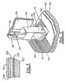
- Figure 3 depicts an SEM taken at a 70° tilt from perpendicular of a regrown CdS layer 84 formed over a tin oxide layer 82.
- a small pin hole in the tin oxide layer such as pin hole 86, does not dramatically affect the efficiency of the photovoltaic cell, since a uniform conductive layer is nevertheless provided under the CdS layer.
- the film layer shown on Figure 3 is approximately 7 microns thick, and it can be seen that the top surface of the layer and the bottom surface of the layer are each substantially defined by the upper and lower surfaces of crystals.
- a single layer or monolayer of crystals having a substantially uniform crystal height is thus produced according to the concepts of the present invention.
- Each of the individual crystals 84A-84G thus has a substantially planar lower surface in engagement with the tin oxide layer, and a substantially planar upper surface. These surfaces, together with similarly situated surfaces of other crystals, thus form the lower and upper surface of the CdS film, respectively.
- Crystals 84A, 84C, 84D and 84H each have both lengths and widths greater than their 7 micron height, and thus have a mean diameter in excess of 7 microns.
- Crystals 84B and 84E each have a length and width substantially equal to their 7 micron height, and thus have a mean diameter approximating the thickness of the CdS layer.
- crystals 84E and 84G appear to have a length and a width somewhat smaller than their height, and thus would have a mean diameter slightly less than the film thickness. As can be seen in Figure 3, however, a majority of the crystals have a mean diameter in excess of, or at least substantially equal to, the film thickness.
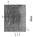
- Figure 4 is a SEM at a larger magnification of crystal 84G shown in Figure 3.
- Each of the crystals in the CdS layer thus has a substantially planar lower surface 90 in engagement with the tin oxide film layer 82, and a substantially planar upper surface 92.
- the sides of the crystal comprise a plurality of substantially vertical walls 94 which together define an irregular configuration.
- Figure 4 also depicts that, although the upper and lower surfaces of the crystals are somewhat rounded where the surface meet the walls, only a very slight gap 88 exists between adjacent crystals. This small or non-existing gap between adjacent crystals eliminates or at least substantially reduces the likelihood of short circuiting between the tin oxide layer and the layer overlying the CdS layer added to form the photovoltaic cell.
- the approximately 12 micron thickness compressed CdS film, one regrown, results in the CdS layer having a thickness from 4 to 8 microns, and preferably from 5 to 7 microns.
- the CdS layer formed according to the present invention is thus much thinner, and therefore less costly, than a film having a thickness of from 20 to 30 microns produced according to silkscreening techniques.
- the polycrystalline semi-conductor film formed according to the present invention is particularly suitable for forming a CdS layer for a photovoltaic cell of the backwall configuration.
- the above-described layer may be utilized to form a CdS/Cu2S photovoltaic cell according to the teachings of U.S.-A-4, 362, 896.
- the above described CdS film to form a high efficiency and low manufacturing cost cadmium sulfide/cadmium telluride photovoltaic cell.
- Figure 5 depicts a simplified cross-sectional view of a photovoltaic cell formed according to the present invention, and including the improved cadmium sulfide layer described above.
- the back-wall cell is suitable for large scale production of photovoltaic cells on an economic basis, and is formed on a planar glass substrate 102 having any desired thickness, e.g. 317.5 ⁇ 10 ⁇ 3 cm (0.125 in).
- the cell includes a conductive tin oxide layer 104 having a thickness of approximately .7 microns or less, a CdS layer 106 of from 4 to 8 microns in thickness, a second polycrystalline layer 108 having a thickness of from 1 to 4 microns and suitable for forming the photovoltaic heterojunction with the CdS layer, and an electrode layer 110 in contact with the second layer and having a thickness of from .5 to 2 microns.
- the second polycrystalline layer may be a cuprous sulfide layer formed according to the teachings of the '896 patent.
- the second layer comprises cadmium telluride.
- Panels of cadmium sulfide/cadmium telluride photovoltaic cells having dimensions of approximately 30.5 cm X 30.5 cm (12 in X 12 in) may thus be formed from glass substrate panels of the same or slightly larger dimensions.
- the photovoltaic panels may be separated into elongated strips of interconnected photovoltaic cells according to the teachings of U.S.-A-4,262,411. The panels may then be combined electrically in parallel or in series to form modules.
Landscapes
- Photovoltaic Devices (AREA)
Description
- The present invention relates to the formation of thin film semiconductor layers and, more particularly, the formation of a thin film polycrystalline CdS layer having large diameter crystals and suitable for manufacturing photovoltaic cells.
- Solar energy has long been recognized as an alternative to traditional hydrocarbon energy sources, and the direct conversion of solar radiation to electricity via the photovoltaic process is a growing field for research and development. Currently marketed photovoltaic devices have, however, achieved only limited acceptance in specialized industries, such as expensive telecommunications installations, lighted buoys having low electrical consumption, and outer space applications.
- In view of the significant costs of manufacturing single crystal photovoltaic cells, significant efforts have been ongoing for the past 20 years to develop a low cost polycrystalline photovoltaic cell. Tremendous financial investments have been and are continuing in the commercialization of polycrystalline and amorphous silicon solar cells, and also polycrystalline cadmium sulfide solar cells. Unfortunately, such cells inherently have a lower efficiency than single crystal cells, and the high capital investment and significant manufacturing costs for producing such cells according to current manufacturing technology have substantially inhibited market acceptance.
- One promising approach to mass production of polycrystalline solar energy devices at a low cost utilizes a transparent vitreous substrate, such as common float glass, with photovoltaic films formed in successive layers on the substrate. In one "back wall" arrangement disclosed in U.S.-A-4,362,896, thin film layers of tin oxide, cadmium sulfide, cuprous sulfide, and an electrode material are applied to form the cell, with radiant energy passing through the glass and tin oxide layers before being absorbed in the CdS/Cu₂S heterojunction. In another similar polycrystalline photovoltaic cell, cadmium telluride is utilized in place of cuprous sulfide.
- In order to achieve low cost manufacturing of such cells, the cadmium sulfide layer must be relatively thin, i.e., less than 10 microns. Also, it has been found that the formation of the cadmium sulfide layer by spray pyrolysis techniques, such as are disclosed in U.S.-A-4,338,078, are difficult to control. The varying temperatures of the glass substrate surface results in poor yield rates, which in turn significantly increases manufacturing costs.
- Methods and apparatus are provided for forming improved polycrystalline semiconductor film on a rigid substrate. According to a preferred embodiment of the invention, a thin monolayer CdS film is formed on a glass substrate. The subsequent application of additional film layers produces an inexpensive photovoltaic cell of the back wall configuration.
- The CdS film is formed by mixing a fine powder of cadmium sulfide and a liquid carrier, such a propylene glycol, to form a slurry of a desired texture. An exemplary slurry comprises approximately 60 grams of cadmium sulfide, 2 grams of cadmium chloride (which acts as a flux in the regrowth), and 100 grams of propylene glycol. The slurry is then sprayed or otherwise deposited on a glass substrate at room temperature. The film is dried, preferably in air at a temperature near the boiling point of the carrier. The film is then compressed by the application of significant mechanical force in the range of from 34.47·10⁶ Pa (5,000 psi) to 68.95·10⁶ Pa (10,000 psi). The compressed film is then regrown in a heated mixture of inert gas and oxygen, using the chloride as a flux to assist in crystal growth. This method produces crystals having a much larger diameter than those produced according to the spray pyrolysis techniques of U.S.-A-4,338,078.
- According to one technique, the dried film is compressed by moving the glass substrate horizontally with respect to a plurality of vertically movable rollers, each actuated by a hydraulic fluid-powered cylinder. The glass travels under the rollers, resulting in compressed strips of CdS film. The cylinders are raised, the glass indexed to the next position, the cylinders lowered, and the glass again passed under the cylinders, resulting in overlapping strips of compressed film. The process is continued until substantially the entirety of the CdS film has been compressed.
- The CdS film according to the present invention generally has thickness less than 10 microns, and preferably in the range of from 4 to 8 microns. Many of the individual regrown crystals have a pancake-shaped configuration, with the top and bottom surfaces being defined by the upper and lower surfaces of the CdS film. A CdS film monolayer of single crystals between the upper and lower surfaces of the film is thus formed, with most crystals having a length and width substantially greater than their height. A relatively small gap is obtained between adjacent crystals, so that the subsequent application of another film layer for forming a a photovoltaic cell generally does not result in an unacceptable degree of short circuits through the CdS film.
- The manufacturing costs of producing the CdS layer is substantially reduced since neither expensive deposition equipment nor difficult quality control parameters, such as uniformly heating glass to an exact temperature, are utilized. The efficiency of the photovoltaic cell is substantially improved, since large crystals, many having a mean diameter in excess of the film thickness, are obtained. According to one technique, the film of the present invention is utilized to form a high quality, low cost CdS/CdTe photovoltaic cell.
- Figure 1 is a pictorial view of apparatus suitable for compressing the CdS film according to the present invention.
- Figure 2 is a pictorial view of a portion of the apparatus depicted in Figure 1, with the glass substrate and CdS film shown in cross-section.
- Figure 3 is a pictorial view of regrown cadmium sulfide crystal layer on a glass substrate manufactured according to the techniques of the present invention.
- Figure 4 is a more detailed pictorial view of regrown cadmium sulfide crystals shown in Figure 3.
- Figure 5 is a simplified cross-sectional view of a portion of a photovoltaic cell manufactured according to the present invention.
- The cadmium sulfide film layer formed according to the present invention may be applied to any suitable rigid substrate material. According to a preferred teaching of the invention, the layer is utilized in forming a photovoltaic cell of the back wall configuration, and accordingly the CdS layer is formed over a transparent vitreous substrate coated with a thin-layer transparent conductive material, such as tin oxide.
- Since reduced product cost is a significant feature of the present invention, the vitreous substrate preferably is common window glass formed by the process wherein a glass ribbon floats on a hot tin bath. A conductive tin oxide film with a high transmissivity is applied to a surface of the float glass. The tin oxide film may be formed either when the glass is floated on the tin bath, as disclosed in U.S.-A-3,959,565, or may be sprayed on radiantly heated glass panels according to the teachings of U.S.-A-4,224,355, each hereby incorporated by reference.
- The desired tin oxide film has a sheet resistance of less than 10 ohms per square, absorbs less than 10% of the incident visible light spectrum which produces solar energy by the photovoltaic process, and has a emissivity of less than .1 for infrared radiation having wavelengths greater than 5 microns (up to a temperature of 350°C). Moreover, minute pin holes in such a tin oxide film, although a serious drawback to the formation of conductive tin patterns on a glass panel, are not a significant drawback to the efficiency of polycrystalline photovoltaic cells. In addition to low cost, such a conductive tin oxide film is also tightly adherent to the glass substrate, sufficiently hard to withstand the partial removal of overlying layers, chemically inert at elevated temperatures and exposure to ultraviolet irradiation, and free of impurities which might affect CdS layer formation.
- The glass is preferably washed with deionized water both before the tin oxide spraying process and prior to the application of the CdS layer. As those skilled in the art recognize, reasonable care must be taken to avoid contamination of the film layers which form the photovoltaic cell in order to maintain high cell efficiency and good production yields.
- A CdS slurry is prepared utilizing commercially available cadmium sulfide powder having a powder size of 2 microns or less. A small amount of cadmium chloride is added to provide the desired flux to enhance crystal growth during the regrowth stage. A suitable carrier, such as propylene glycol terpineol, is used to achieve the desired slurry texture. The desired texture will, in part, depend on the application technique and the application equipment. For an ambient air spraying operation, a mixture of approximately 60 grams of cadmium sulfide, 2 grams of cadmium chloride, and 100 grams of propylene glycol has been found acceptable. As those skilled in the art recognize, a small amount of chloride facilitates crystal growth, although a chloride level in excess of that required to react with the cadmium sulfide is deleterious to photovoltaic performance and life. Accordingly, steps should be taken to avoid excessive or residual cadmium chloride. Finally, if cadmium telluride is to be the layer overlying the cadmium sulfide film to form the photovoltaic cell, a small amount (100 to 1000 PPM) of cupric acetate may be added to the slurry to serve as a dopant.
- Assuming spraying techniques are utilized to apply the CdS slurry to the glass substrate previously coated with a tin oxide film, the combination of the carrier material and ambient temperature for both the sprayed slurry and the glass substrate during application substantially decreases application costs and increases the uniformity of an acceptable uniform layer. Various types of conventional spraying techniques and equipment may be utilized to form a uniform layer. The spray process is well adapted to conveyer belt systems, with the spraying accomplished by traversing the spray guns across the width of glass panels laid on the belt, as disclosed in U.S.-A-4,224,355. It has been found that the application of a CdS slurry having a thickness of approximately 20 microns results in a large crystal CdS film of regrown crystals having a thickness of approximately 4 to 7 microns, as described subsequently.
- The CdS slurry may be dried either at less than 60°C at reduced pressure or at approximately 200°C in air. Propylene glycol will evaporate from the layer and, if desired, may be recovered by conventional distillation techniques. The resulting product will be a polycrystalline CdS layer, although substantial voids will exist where the carrier material has evaporated. Moreover, the "as sprayed" CdS crystals will be extremely small in size, and the resultant film is not practical for producing a reasonably efficient photovoltaic cell.
- According to the present invention, the dried CdS film is compressed from approximately 20 microns to a range generally from 10 to 14 microns, and preferably to approximately 12 microns, by the application of a substantial mechanical force. Both the glass substrate and the tin oxide layer can easily withstand the desired compressive force pf generally from 34.47·10⁶ Pa (5,000 psi) to 68.95·10⁶ Pa (10,000 psi), and preferably from 41.37·10⁶ Pa (6,000 psi) to 55.16·10⁶ Pa (8,000 psi). Although the reason for increased cell regrowth due to this prior compressive action is not fully known, the compressive force substantially reduces the voids between CdS material found when the carrier material evaporates. Also, the contact area between the grains of powder is substantially increased by the compressive action, and the increased contact area of the powder grains resulting from compression may be directly related to the desired increased crystal size during regrowth.
- Suitable apparatus for compressing the CdS film layer is shown in Figure 1.
Machine 10 has astandard base 12 and an X-Y table 14. Table 14 may be manually moved in The Y direction by a standard worm screw and handleassembly 16, or may be power driven bydrive motor 18 interconnected to theworm screw 16. Movement or indexing of the table in the X-direction is similarly manually controlled by wormscrew and handleassembly 20, which may be powered bydrive motor 22. - A
panel 24 containing the previously described tin oxide and sprayed cadmium sulfide layers (with the carrier evaporated) may be placed on the table 14, and into engagement with edge strips 26 and 28. If desired, a standard vacuum table containing a plurality of small apertures may be utilized to fixedly position thepanel 24 on the table, and vacuum line is accordingly provided. It has been found,however, that a rolling vertically-applied force to the glass substrate produces a minimal force in any direction of the plane of the substrate, and accordingly a vacuum table may not be required. - A
vertical plate 54 is rigidly mounted to themachine base 12 via asupport 11. A plurality of air/oil cylinders plate 54. Each cylinder is activated in the downward direction by air pressure frominput line 38, and is provided with a correspondinghydraulic fluid line 40 for returning the cylinders to the upward position once air pressure inlines 38 is relieved. Eachcylinder rod 42 thus reciprocates in a vertical path, and preferably all cylinders are simultaneously activated. - Referring now to Figure 2, block 44 is pivotably connected at 56 to
rod 42, and rides within adovetail channel 52 in theplate 54. Two downwardly extendingarms 48 ofblock 44 are used to rotatably mountroller 46 onpin 50.Dovetail 52 thus restrains movement ofblock 44 to substantially a vertical direction, although sufficient "play" is provided betweenblock 44 andplate 54 to enable slight pivotable movement ofblock 44 and thusroller 46 aboutpin 56. This slight pivotable movement of the roller thus ensures that the roller lays "flat" on the glass substrate during the compression operation. - Referring again to Figure 1, air pressure at approximately 792.9·10³ Pa (115 psi) is supplied by
lines 38 from a suitable source (not shown) to causerollers 46 to engage and exert a downward force on the CdS film. A typical stainless steel roller has a diameter of approximately 3.81 cm (1.5 in) and a width of 1.016 cm (0.4 in), resulting in an instantaneous compressed area of 127·10⁻³ cm (0.05 in) X 1.016 cm (0.4 in) for each roller. The downward force exerted by each roller is approximately 756,2 N (170 pounds), so that the compressional force on the CdS film is approximately 55.16·10⁶ Pa (8,000 psi). - Once the cylinders have been activated to force the rollers downward into engagement with the substrate,
motor 18 may be activated to rotate Y-direction table screw 16 to move table 14 and form a plurality of strips of compressed CdS film. Once stop 58 affixed to table 14 engages limits switch 62 affixed tobase 12, rotation ofscrew 16 is terminated and air pressure to the cylinders is exhausted, allowing hydraulic fluid inlines 40 to raise the cylinders. Once raised, the table may be indexed by activatingmotor 22 to rotate screw 20 a sufficient number of turns to approximate the width of the compressed strip. The table may then be returned to the position shown in Figure 1, and when stop 58 engages limits switch 60 to process is repeated. If desired,machine 10 could be easily adapted to compress film while the table travels in both the forward and reverse Y directions. - Figure 2 thus illustrates a plurality of
compressed strips 70 of CdS film overlying the thintin oxide layer 82 on theglass substrate 80. Preferably asmall overlap 74 of compressed strips is utilized, since such an overlap is not deleterious to the subsequent film layer regrowth operation, and ensures that all the film is compressed. Figure 2 also illustrates that theroller edge 72 of each strip is spaced slightly, e.g. 635·10⁻³ cm (¼ in), from the edge of the glass to ensure that the glass does not crack when the roller is first lowered. - Any minute particles on the CdS film may adversely affect the compression process, and typically result in a thin horizontal strip of film not sufficiently compressed because the roller was raised slightly by the particle. It has been found, however, that sufficient care can be taken to eliminate or substantially reduce the deposition of such particles on the CdS film. Alternatively, the film may be easily cleaned by compressed air to remove such particles from the film prior to compression. A
compressed air nozzle 78 is accordingly provided for blowing such particles off the substrate before the table is indexed to that location. A suitable air/hydraulic fluid cylinder is part No. Y5528 (No. 603) manufactured by PHD, Inc., with offices in Fort Wayne, Indiana. - After the CdS layer of
panel 24 has been compressed, the film is regrown, preferably in a nitrogen rich atmosphere, according to the techniques similar to those described in U.S.-A-4,362,896, hereby incorporated by reference. In particular, the CdS film is preferably regrown in the heated atmosphere containing cadmium chloride vapors. This is accomplished by vertically positioning film layers of adjacent panels in a face-to-face spaced apart relationship within the heated atmosphere to produce the desired crystals. Unlike CdS crystals obtained according to the '896 patent, however, many of the crystals formed according to the present invention have dimensions in excess of 10 microns, and most if not all crystals have dimensions substantially in excess of from 1 to 2 microns. Moreover, the cost of forming the CdS layer has been substantially reduced compared to spray pyrolysis, because no attempt is made to heat the glass to a uniform elevated temperature while spraying the CdS material on the glass. Also, zinc may be added to form an improved voltage (ZnxCd1-x)S film for some photovoltaic device structure. - The CdS film typically may be heated at a temperature of from 480°C to 580°C, and preferably at approximately 530°C, in a nitrogen atmosphere containing from about 1% to about 3% oxygen. The glass panels are heated for approximately one hour, then cooled down over a period of approximately 45 minutes. The desired cadmium chloride vapors evolve from the film and contribute to the desired crystal growth. After being regrown, the CdS film may be rinsed with methanol and then subsequently rinsed in water to remove excess cadmium chloride on the surface of the CdS film.
- Figure 3 depicts an SEM taken at a 70° tilt from perpendicular of a regrown
CdS layer 84 formed over atin oxide layer 82. As previously indicated, a small pin hole in the tin oxide layer, such aspin hole 86, does not dramatically affect the efficiency of the photovoltaic cell, since a uniform conductive layer is nevertheless provided under the CdS layer. - The film layer shown on Figure 3 is approximately 7 microns thick, and it can be seen that the top surface of the layer and the bottom surface of the layer are each substantially defined by the upper and lower surfaces of crystals. A single layer or monolayer of crystals having a substantially uniform crystal height is thus produced according to the concepts of the present invention. Each of the
individual crystals 84A-84G thus has a substantially planar lower surface in engagement with the tin oxide layer, and a substantially planar upper surface. These surfaces, together with similarly situated surfaces of other crystals, thus form the lower and upper surface of the CdS film, respectively. -
Crystals Crystals 84B and 84E each have a length and width substantially equal to their 7 micron height, and thus have a mean diameter approximating the thickness of the CdS layer. Finally,crystals - Figure 4 is a SEM at a larger magnification of
crystal 84G shown in Figure 3. Each of the crystals in the CdS layer thus has a substantially planarlower surface 90 in engagement with the tinoxide film layer 82, and a substantially planarupper surface 92. The sides of the crystal comprise a plurality of substantiallyvertical walls 94 which together define an irregular configuration. Figure 4 also depicts that, although the upper and lower surfaces of the crystals are somewhat rounded where the surface meet the walls, only a veryslight gap 88 exists between adjacent crystals. This small or non-existing gap between adjacent crystals eliminates or at least substantially reduces the likelihood of short circuiting between the tin oxide layer and the layer overlying the CdS layer added to form the photovoltaic cell. - The approximately 12 micron thickness compressed CdS film, one regrown, results in the CdS layer having a thickness from 4 to 8 microns, and preferably from 5 to 7 microns. The CdS layer formed according to the present invention is thus much thinner, and therefore less costly, than a film having a thickness of from 20 to 30 microns produced according to silkscreening techniques.
- The polycrystalline semi-conductor film formed according to the present invention is particularly suitable for forming a CdS layer for a photovoltaic cell of the backwall configuration. Thus, the above-described layer may be utilized to form a CdS/Cu₂S photovoltaic cell according to the teachings of U.S.-A-4, 362, 896. Also, as a particular feature of the present invention to utilize the above described CdS film to form a high efficiency and low manufacturing cost cadmium sulfide/cadmium telluride photovoltaic cell.
- Figure 5 depicts a simplified cross-sectional view of a photovoltaic cell formed according to the present invention, and including the improved cadmium sulfide layer described above. The back-wall cell is suitable for large scale production of photovoltaic cells on an economic basis, and is formed on a
planar glass substrate 102 having any desired thickness, e.g. 317.5·10⁻³ cm (0.125 in). The cell includes a conductivetin oxide layer 104 having a thickness of approximately .7 microns or less, aCdS layer 106 of from 4 to 8 microns in thickness, a secondpolycrystalline layer 108 having a thickness of from 1 to 4 microns and suitable for forming the photovoltaic heterojunction with the CdS layer, and anelectrode layer 110 in contact with the second layer and having a thickness of from .5 to 2 microns. - According to the present invention, the second polycrystalline layer may be a cuprous sulfide layer formed according to the teachings of the '896 patent. According to a preferred embodiment of the invention, the second layer comprises cadmium telluride. Panels of cadmium sulfide/cadmium telluride photovoltaic cells having dimensions of approximately 30.5 cm X 30.5 cm (12 in
X 12 in) may thus be formed from glass substrate panels of the same or slightly larger dimensions. The photovoltaic panels may be separated into elongated strips of interconnected photovoltaic cells according to the teachings of U.S.-A-4,262,411. The panels may then be combined electrically in parallel or in series to form modules. - Although the invention has been described in terms of the specified embodiments which are set forth in detail, it should be understood that this is by illustration only and that the invention is not necessarily limited thereto, since alternative embodiments and operating techniques will become apparent to those skilled in the art in view of the disclosure.
Claims (11)
- A process of forming improved polycrystalline semi-conductor films which are to be formed on the electrically conductive surface of a transparent glass substrate in a photovoltaic cell of a backwall configuration, comprising the steps of
mixing a CdS-powder suitable for forming the polycrystalline layer and a liquid carrier to form a slurry of a desired consistency,
applying said CdS-slurry on said substrate while at ambient temperature,
evaporating at least substantially the entirety of the liquid carrier to form a polycrystalline CdS-film on a substrate having relatively small diameter crystals,
applying a compressive force to the polycrystalline film to reduce the film thickness by 50 to 70% and
heating the compressed film and substrate to form a semiconductor film comprised of relatively larger CdS-crystals having a mean diameter equal or greater than the thickness of the film after heating. - A process as defined in Claim 1, wherein the slurry is sprayed on the substrate while the substrate is in substantially horizontal plane.
- A process as defined in Claim 2, further comprising the step of
arranging a series of substrate panels on a horizontally moving conveyer belt; and spraying the slurry from one or more guns positioned above the conveyer belt and moving traversely with respect to the moving substrate panels. - A process as defined in Claims 1 to 3, wherein the applied slurry is dried at a temperature between ambient temperature and the liquid carrier boiling point.
- A process as defined in Claim 1, wherein the compressive force is in excess of 34.47 x 10⁶ Pa (5,000 psi) and less than 68.95 x 10⁶ Pa (10,000 psi).
- A process as defined in Claim 1 and 5, wherein the compressive force is in the range of 41.37 x 10⁶ Pa (6,000 p.s.i.) and 55.16 x 10⁶ Pa (8,000 psi).
- A process as defined in Claim 1, 5 and 6, wherein the compressive force is applied to the film by one or more rollers exerting a force perpendicular to the plane of the substrate.
- A process as defined in Claim 1, wherein the step of heating the compressed film comprises:
positioning one or more glass substrates in a substantially vertical plane;
and thereafter heating the substrate in an atmosphere containing an inert gas and at a temperature in excess of 480°C. - A process as defined in Claims 1 to 8, wherein:
the step of mixing the slurry includes mixing a flux with the cadmium sulfide powder and the liquid carrier. - A process as defined in Claims 8 or 9, wherein the step of positioning the glass substrate in a vertical plane includes positioning the polycrystalline cadmium sulfide film layers in a face-to-face relationship for maintaining a desired concentration of flux vapor.
- A process as defined in Claim 9, wherein the flux is cadmium chloride.
Applications Claiming Priority (2)
| Application Number | Priority Date | Filing Date | Title |
|---|---|---|---|
| US06/918,115 US4735909A (en) | 1986-10-14 | 1986-10-14 | Method for forming a polycrystalline monolayer |
| US918115 | 1986-10-14 |
Publications (3)
| Publication Number | Publication Date |
|---|---|
| EP0264739A2 EP0264739A2 (en) | 1988-04-27 |
| EP0264739A3 EP0264739A3 (en) | 1989-04-12 |
| EP0264739B1 true EP0264739B1 (en) | 1993-03-10 |
Family
ID=25439834
Family Applications (1)
| Application Number | Title | Priority Date | Filing Date |
|---|---|---|---|
| EP87114766A Expired - Lifetime EP0264739B1 (en) | 1986-10-14 | 1987-10-09 | Method and apparatus for forming a polycristalline monolayer |
Country Status (6)
| Country | Link |
|---|---|
| US (1) | US4735909A (en) |
| EP (1) | EP0264739B1 (en) |
| AU (1) | AU588772B2 (en) |
| BR (1) | BR8705452A (en) |
| CA (1) | CA1325161C (en) |
| DE (1) | DE3784616T2 (en) |
Families Citing this family (12)
| Publication number | Priority date | Publication date | Assignee | Title |
|---|---|---|---|---|
| US4828876A (en) * | 1985-02-06 | 1989-05-09 | Sharp Kabushiki Kaisha | Production of photoelectric conversion film and contact type image sensor |
| US5022930A (en) * | 1989-06-20 | 1991-06-11 | Photon Energy, Inc. | Thin film photovoltaic panel and method |
| US5501744A (en) * | 1992-01-13 | 1996-03-26 | Photon Energy, Inc. | Photovoltaic cell having a p-type polycrystalline layer with large crystals |
| US5261968A (en) * | 1992-01-13 | 1993-11-16 | Photon Energy, Inc. | Photovoltaic cell and method |
| US5279678A (en) * | 1992-01-13 | 1994-01-18 | Photon Energy, Inc. | Photovoltaic cell with thin CS layer |
| EP0586215B1 (en) * | 1992-08-31 | 1997-04-23 | Research Development Corporation of Japan | Method for manufacturing a fine-particle two-dimensional assembly and apparatus therefor |
| JPH06163954A (en) * | 1992-11-20 | 1994-06-10 | Sanyo Electric Co Ltd | Method of forming crystalline silicon thin film and photovoltaic device using the film |
| US5491114A (en) * | 1994-03-24 | 1996-02-13 | Starfire Electronic Development & Marketing, Ltd. | Method of making large-area semiconductor thin films formed at low temperature using nanocrystal presursors |
| DE4415132C2 (en) * | 1994-04-29 | 1997-03-20 | Siemens Ag | Process for shaping thin wafers and solar cells from crystalline silicon |
| ATE381785T1 (en) * | 2000-07-26 | 2008-01-15 | Antec Solar Energy Ag | METHOD FOR ACTIVATING CDTE THIN FILM SOLAR CELLS |
| JP2009510724A (en) * | 2005-09-23 | 2009-03-12 | トム ラスト, | Photovoltaic device manufacturing system and method |
| EP2239786A1 (en) * | 2009-04-09 | 2010-10-13 | Von Roll Solar AG | High efficiency photovoltaic device, photovoltaic panel and manufacturing method thereof |
Family Cites Families (4)
| Publication number | Priority date | Publication date | Assignee | Title |
|---|---|---|---|---|
| IL56418A (en) * | 1978-03-15 | 1982-02-28 | Photon Power Inc | Method and apparatus for film formation on glass substrates by spraying |
| US4362896A (en) * | 1980-10-28 | 1982-12-07 | Photon Power, Inc. | Polycrystalline photovoltaic cell |
| US4388483A (en) * | 1981-09-08 | 1983-06-14 | Monosolar, Inc. | Thin film heterojunction photovoltaic cells and methods of making the same |
| CA1207421A (en) * | 1983-11-14 | 1986-07-08 | Ottilia F. Toth | High efficiency stable cds cu.sub.2s solar cells manufacturing process using thick film methodology |
-
1986
- 1986-10-14 US US06/918,115 patent/US4735909A/en not_active Expired - Fee Related
-
1987
- 1987-10-09 EP EP87114766A patent/EP0264739B1/en not_active Expired - Lifetime
- 1987-10-09 DE DE8787114766T patent/DE3784616T2/en not_active Expired - Fee Related
- 1987-10-13 CA CA000549146A patent/CA1325161C/en not_active Expired - Fee Related
- 1987-10-13 BR BR8705452A patent/BR8705452A/en not_active IP Right Cessation
- 1987-10-13 AU AU79736/87A patent/AU588772B2/en not_active Ceased
Also Published As
| Publication number | Publication date |
|---|---|
| DE3784616T2 (en) | 1993-07-01 |
| EP0264739A3 (en) | 1989-04-12 |
| CA1325161C (en) | 1993-12-14 |
| AU588772B2 (en) | 1989-09-21 |
| DE3784616D1 (en) | 1993-04-15 |
| BR8705452A (en) | 1988-05-24 |
| US4735909A (en) | 1988-04-05 |
| AU7973687A (en) | 1988-04-21 |
| EP0264739A2 (en) | 1988-04-27 |
Similar Documents
| Publication | Publication Date | Title |
|---|---|---|
| US5131954A (en) | Monolithic solar cell array and method for its manufacturing | |
| US5441577A (en) | Thin film solar cell and production method therefor | |
| KR101274660B1 (en) | Method for continuously depositing high resistance buffer layer/window layer(transparent conductive film) of CIS based thin film solar cell and continuous film deposition equipment for carrying out that method | |
| US4735909A (en) | Method for forming a polycrystalline monolayer | |
| US5578502A (en) | Photovoltaic cell manufacturing process | |
| US20020117199A1 (en) | Process for producing photovoltaic devices | |
| KR100343241B1 (en) | Method for producing photovoltaic element | |
| WO1993014523A1 (en) | PHOTOVOLTAIC CELL WITH THIN CdS LAYER | |
| KR20150082525A (en) | Molybdenum substrates for cigs photovoltaic devices | |
| US20080149179A1 (en) | Process for Large-Scale Production of Cdte/Cds Thin Film Solar Cells, Without the Use of Cdci2 | |
| EP2402478B1 (en) | Method of forming a conductive transparent oxide film. | |
| KR101582200B1 (en) | A method for preparing CZTS thin film for solar cell | |
| JP2000044238A (en) | Method for producing tin dioxide film and solar cell | |
| EP1160879A2 (en) | Method of forming silicon-based thin film, silicon-based thin film and photovoltaic element | |
| Bayhan et al. | Eects of Post Deposition Treatments on Vacuum Evaporated CdTe Thin Films and CdS= CdTe Heterojunction Devices | |
| KR101969976B1 (en) | Method for Producing CIGS Thin-Film, CIGS Thin-Film Produced by the Method and Solar Cell Having the Same | |
| JP3504838B2 (en) | Amorphous silicon solar cell | |
| KR20100062269A (en) | Method for manufacturing thin film type solar cell | |
| JP2726323B2 (en) | Thin-film solar cell fabrication method | |
| EP2405030A2 (en) | Selectively deposited thin film devices and methods for forming selectively deposited thin films | |
| JPH01122938A (en) | Method and apparatus for producing polycrystalline film | |
| CN121604709A (en) | Heating device and preparation method of perovskite battery | |
| CN116657107A (en) | A kind of Cu4O3 film and its preparation method and application | |
| JPH11121778A (en) | Method for manufacturing compound semiconductor film and solar cell | |
| AU662802C (en) | Photovoltaic cell with conductive layer for forming a power producing heterojunction |
Legal Events
| Date | Code | Title | Description |
|---|---|---|---|
| PUAI | Public reference made under article 153(3) epc to a published international application that has entered the european phase |
Free format text: ORIGINAL CODE: 0009012 |
|
| AK | Designated contracting states |
Kind code of ref document: A2 Designated state(s): BE CH DE FR GB IT LI NL SE |
|
| PUAL | Search report despatched |
Free format text: ORIGINAL CODE: 0009013 |
|
| AK | Designated contracting states |
Kind code of ref document: A3 Designated state(s): BE CH DE FR GB IT LI NL SE |
|
| 17P | Request for examination filed |
Effective date: 19890914 |
|
| 17Q | First examination report despatched |
Effective date: 19901123 |
|
| GRAA | (expected) grant |
Free format text: ORIGINAL CODE: 0009210 |
|
| AK | Designated contracting states |
Kind code of ref document: B1 Designated state(s): BE CH DE FR GB IT LI NL SE |
|
| PG25 | Lapsed in a contracting state [announced via postgrant information from national office to epo] |
Ref country code: SE Effective date: 19930310 |
|
| REF | Corresponds to: |
Ref document number: 3784616 Country of ref document: DE Date of ref document: 19930415 |
|
| RAP2 | Party data changed (patent owner data changed or rights of a patent transferred) |
Owner name: PHOTON ENERGY, INC. D/B/A GOLDEN PHOTON, INC. |
|
| ITF | It: translation for a ep patent filed | ||
| ET | Fr: translation filed | ||
| NLT2 | Nl: modifications (of names), taken from the european patent patent bulletin |
Owner name: PHOTON ENERGY, INC. D/B/A GOLDEN PHOTON, INC. TE G |
|
| NLXE | Nl: other communications concerning ep-patents (part 3 heading xe) |
Free format text: PAT.BUL.12/93 PAGES 1807 AND 1825:CORR.:PHOTON ENERGY, INC. D/B/A/ GOLDEN PHOTON, INC. PAT.BUL.14/93 PAGE 2154 SHOULD BE DELETED |
|
| PLBE | No opposition filed within time limit |
Free format text: ORIGINAL CODE: 0009261 |
|
| STAA | Information on the status of an ep patent application or granted ep patent |
Free format text: STATUS: NO OPPOSITION FILED WITHIN TIME LIMIT |
|
| 26N | No opposition filed | ||
| PGFP | Annual fee paid to national office [announced via postgrant information from national office to epo] |
Ref country code: CH Payment date: 19941014 Year of fee payment: 8 |
|
| PGFP | Annual fee paid to national office [announced via postgrant information from national office to epo] |
Ref country code: NL Payment date: 19941031 Year of fee payment: 8 |
|
| PGFP | Annual fee paid to national office [announced via postgrant information from national office to epo] |
Ref country code: BE Payment date: 19941208 Year of fee payment: 8 |
|
| PG25 | Lapsed in a contracting state [announced via postgrant information from national office to epo] |
Ref country code: LI Effective date: 19951031 Ref country code: CH Effective date: 19951031 Ref country code: BE Effective date: 19951031 |
|
| BERE | Be: lapsed |
Owner name: PHOTON ENERGY INC. D/B/A GOLDEN PHOTON INC. Effective date: 19951031 |
|
| PG25 | Lapsed in a contracting state [announced via postgrant information from national office to epo] |
Ref country code: NL Effective date: 19960501 |
|
| REG | Reference to a national code |
Ref country code: CH Ref legal event code: PL |
|
| NLV4 | Nl: lapsed or anulled due to non-payment of the annual fee |
Effective date: 19960501 |
|
| PGFP | Annual fee paid to national office [announced via postgrant information from national office to epo] |
Ref country code: FR Payment date: 19960913 Year of fee payment: 10 |
|
| PGFP | Annual fee paid to national office [announced via postgrant information from national office to epo] |
Ref country code: GB Payment date: 19960925 Year of fee payment: 10 |
|
| PGFP | Annual fee paid to national office [announced via postgrant information from national office to epo] |
Ref country code: DE Payment date: 19961018 Year of fee payment: 10 |
|
| PG25 | Lapsed in a contracting state [announced via postgrant information from national office to epo] |
Ref country code: GB Free format text: LAPSE BECAUSE OF NON-PAYMENT OF DUE FEES Effective date: 19971009 |
|
| PG25 | Lapsed in a contracting state [announced via postgrant information from national office to epo] |
Ref country code: FR Free format text: THE PATENT HAS BEEN ANNULLED BY A DECISION OF A NATIONAL AUTHORITY Effective date: 19971031 |
|
| GBPC | Gb: european patent ceased through non-payment of renewal fee |
Effective date: 19971009 |
|
| PG25 | Lapsed in a contracting state [announced via postgrant information from national office to epo] |
Ref country code: DE Free format text: LAPSE BECAUSE OF NON-PAYMENT OF DUE FEES Effective date: 19980701 |
|
| REG | Reference to a national code |
Ref country code: FR Ref legal event code: ST |
|
| PG25 | Lapsed in a contracting state [announced via postgrant information from national office to epo] |
Ref country code: IT Free format text: LAPSE BECAUSE OF NON-PAYMENT OF DUE FEES;WARNING: LAPSES OF ITALIAN PATENTS WITH EFFECTIVE DATE BEFORE 2007 MAY HAVE OCCURRED AT ANY TIME BEFORE 2007. THE CORRECT EFFECTIVE DATE MAY BE DIFFERENT FROM THE ONE RECORDED. Effective date: 20051009 |